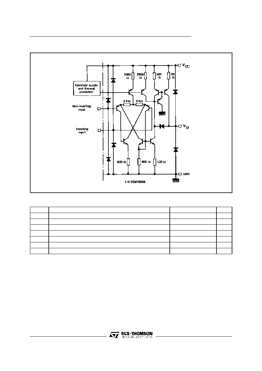
ESM1600B
January 1997
QUAD COMPARATOR INTERFACE CIRCUIT
.
MINIMUM HYSTERESIS VOLTAGE AT EACH
INPUT : 0.3V
.
OUTPUT CURRENT : 15 mA
.
LARGE SUPPLY VOLTAGE RANGE : + 10V to
+ 35V
.
INTERNAL THERMAL PROTECTION
.
INPUT AND OUTPUT CLAMPING PROTEC-
TION DIODES.
DESCRIPTION
The ESM1600Bis a quadruplecomparatorintented
to provide an interface between signal processing
and transmitting lines in very noisy industrial sur-
roundings.
Outputof each comparator,used as line driver, sup-
plies a constant current (PNP output stage) and is
specially well protected against powerful overvol-
tages. The open collector output circuit allows the
connectionof several comparators to a single trans-
mitting line.
The ESM1600B can operate as receiver on a line
transmitting noisy high-voltage signals. Hysteresis
effect, internally implemented on inputs of each
comparator provides an excellent noise immunity.
In addition, each input is also protected against
overvoltages.
The ESM1600B can operate in a wide supply vol-
tage range (standard operational amplifier
±
15 V
supply or single + 12 V or + 24 V supplies used in
industrial electronic sets).
Moreover, internal thermal protection circuitry cuts
out the output current of the four comparators when
power dissipation becomes excessive.
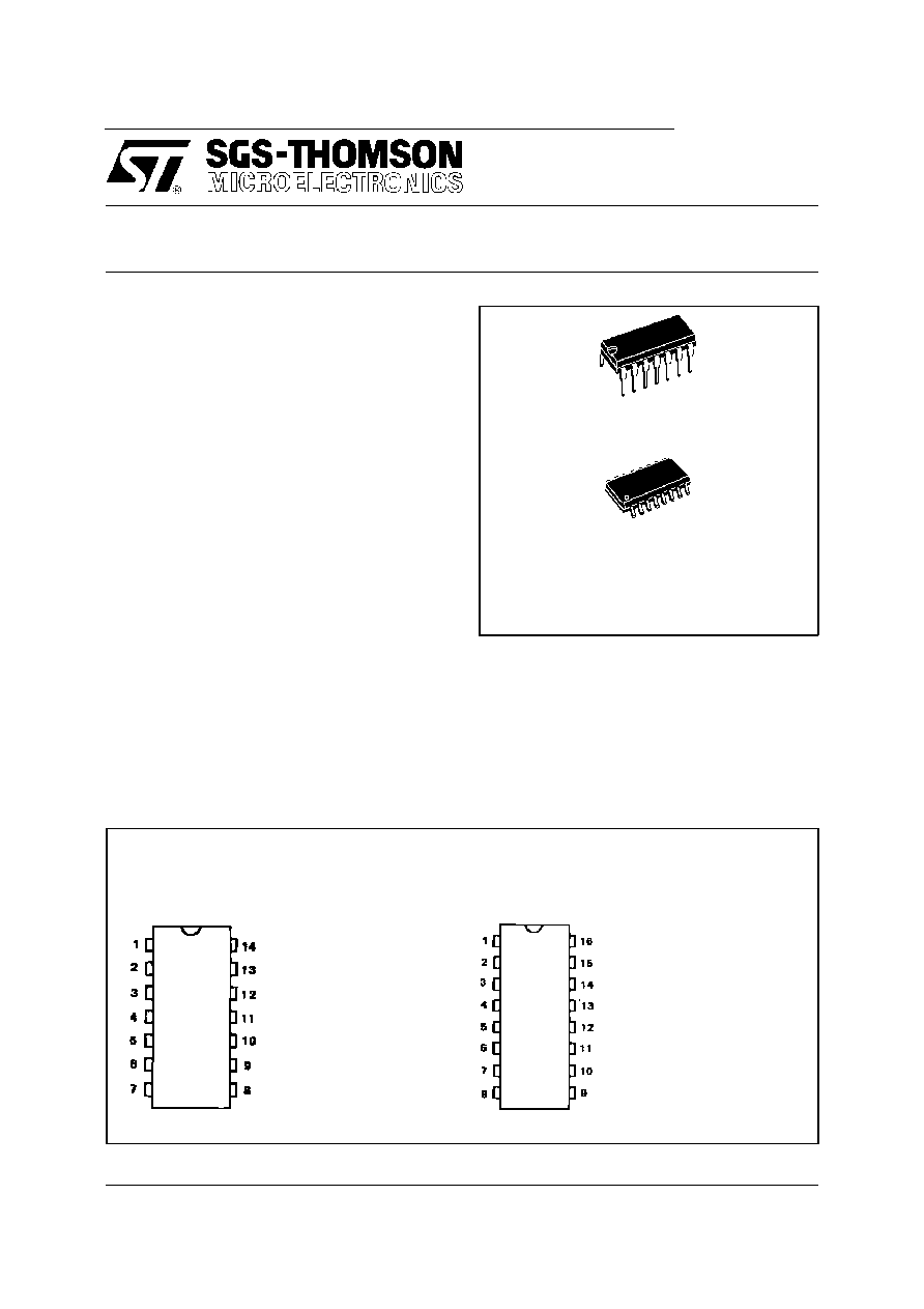
DIP1 4
SO16
DIP14
SO16
1 - Inverting input 1
2 - Non-inverting input 1
3 - Output 1
4 - Non-inverting input 2
5 - Inverting input 2
6 - Output 2
7 - GND
8 - Output 3
9 - Inverting input 3
10 - Non-inverting input 3
11 - Output 4
12 - Non-inverting input 4
13 - Inverting input 4
14 - V
CC
1 - Inverting input 1
2 -Non-inverting input 1
3 - Output 1
4 - Non-inverting input 2
5 - Inverting input 2
6 - Output 2
7 - GND
8 - N.C.
9 - N.C.
10 - Output 3
11 - Inverting input 3
12 - Non-inverting input 3
13 - Output 4
14 - Non-inverting input 4
15 - Inverting input 4
16 - V
CC
ORDER ING NUMBERS: ESM1600B (DIP14)
ESM1600BFP (SO16)
PIN CONNECTIONS (to p view)
1/10
ELECTRICAL CHARACTERISTICS
V
CC
= +35V, -25
o
C
T
amb
+85
o
C (unless otherwise specified)
Symbol
Parameter
Min.
Typ.
Max.
Typ.
Fig.
V
I
+
V
I
≠
Input Voltage Range - Note 1
Non-inverting Input
Inverting Input
0
2
33
33
V
V
C
Input Control Voltage (2V < V
CM
< 33V) - Note 2
150
500
mV
1
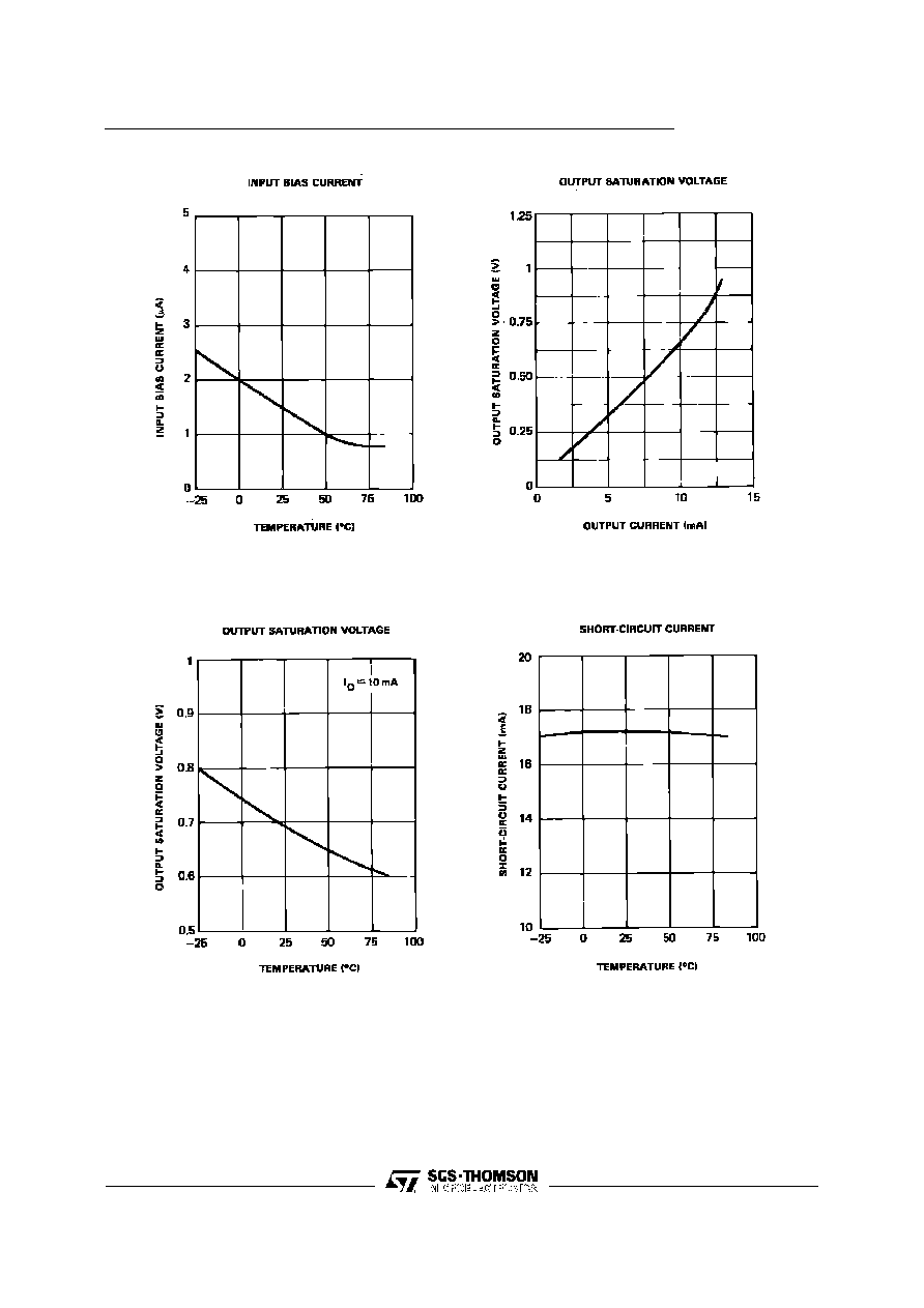
I
IB
Input Bias Current - Note 3
1
5
µ
A
I
SC
Short-circuit Output Current
V
CC
= +10 to +35 V
6
25
mA
2
V
CC
≠V
O
Output Saturation Voltage (high level) - (I
O
= ≠10mA)
1
1.5
V
3
I
OL
I
OH
Output Off-state Current
(V
I
+
= 2V, V
I
≠
= 33V)
1
5
µ
A
4
I
CC
Supply Current
R
L
=
for the 4 Comparators
R
L
Common for the 4 Comparators
3
9
5
12
mA
5
S
VO
Output Slew-rate (R
L
= 3k
, T
amb
= +25
o
C)
1
V/
µ
s
V
F
Input Protective Diode Forward Voltage
(I = 20mA, T
amb
= +25
o
C)
1.5
V
≠
Energy of Pulses against which Circuit Output is Protected
(T
amb
= +25
o
C) - Note 4
20
mJ
≠
Pulsed Current Applied to Protective Output Diodes
(T
amb
= +25
o
C) - Note 5
0.4
A
6
No tes : 1. When negative input is biased between 0 and 2 volts output is always low.
2. Comparator hysteresis voltage on positive input on the one hand and negative input on the other hand equals sum of input control
voltages V
C1
+ V
C2
or V
C3
+ V
C4.
3. Input current flows out of the circuit owing to PNP input stage. This current is constant and independent of output level. So no load
change is transmitted to inputs.
4. By definition, a circuit is immunized against powerful signals when no durable character istic change occurs after the application of
these signals and when the circuit has not been destroyed.
In industrial surroundings, parasitic signals contain usually high voltage (over 200 V) AC harmonics having variable impedance of
500
to 10k
.
The power dissipation of thesesignals is divided between clamping diodes and the V
CC
. Simulationis used to determine the maximum
energy level. The injected current value cannot in any case exceed 3A.
5. Output protective diodes are tested individually by means of positive and negative dischar ge voltages of a capacitor. The negative
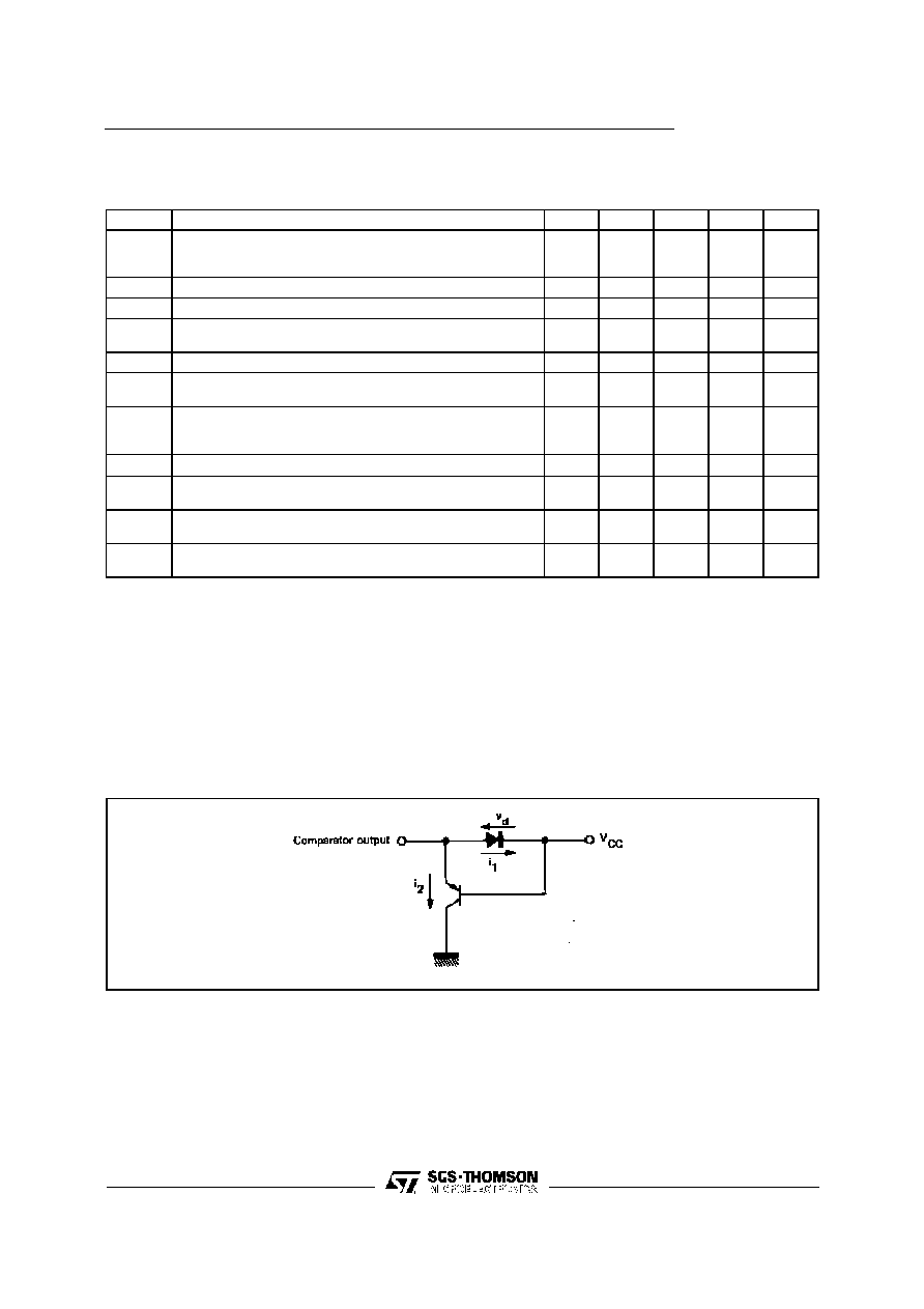
discharge control occurs through a single diode. During positive discharge, due to the properties of integration, a grounded collector
PNP transistor appears in parallel with the clamping diode connected to V
CC
. A part of the current flows through this transistor, V
CE
being greater than V
CC
. If T is the total discharge duration, energy dissipated in the circuit is :
For a certain injected current, the lower the current I
2
, that is to say the lower the PNP current gain the smaller the energy is dissipated in the cir-
cuit. Topology and technological processes have been chosen to shorten this current gain.
W =
T
[ i
1
vd +
i
2 (VCC + vd)
]
dt
O
ESM1600B
3/10