 | –≠–ª–µ–∫—Ç—Ä–æ–Ω–Ω—ã–π –∫–æ–º–ø–æ–Ω–µ–Ω—Ç: ETL9344 | –°–∫–∞—á–∞—Ç—å:  PDF PDF  ZIP ZIP |
ETL9444/ETL9445
ETL9344/ETL9345
May 1989
4-BIT NMOS MICROCONTROLLERS
.
LOW COST
.
POWERFUL INSTRUCTION SET
.
2k x 8 ROM, 128 x 4 RAM
.
23 I/O LINES (ETL9444)
.
TRUE VECTORED INTERRUPT, PLUS RES-
TART
.
THREE-LEVEL SUBROUTINE STACK
.
16
µ
s INSTRUCTION TIME
.
SINGLE SUPPLY OPERATION (4.5-6.3V)
.
LOW CURRENT DRAIN (13mA max.)
.
INTERNAL TIME-BASE COUNTER FOR REAL-
TIME PROCESSING
.
INTERNAL BINARY COUNTER REGISTER
WITH MICROWIRE
Æ
SERIAL I/O CAPABILITY
.
GENERAL PURPOSE AND TRI-STATE
Æ
OUT-
PUTS
.
LSTTL/CMOS COMPATIBLE IN AND OUT
.
DIRECT DRIVE OF LED DIGIT AND SEGMENT
LINES
.
SOFTWARE/HARDWARE
COMPATIBLE
WITH OTHER MEMBERS OF ET9400 FAMILY
.
EXTENDED TEMPERATURE
RANGE DE-
VICES
ETL9344/L9345 (≠ 40
∞
C to + 85
∞
C)
.
WIDER SUPPLY RANGE (4.5 ≠ 9.5V)
OPTIONALLY AVAILABLE
.
SOIC 24/28 AND PLCC 28 PACKAGES AVAI-
LABLE
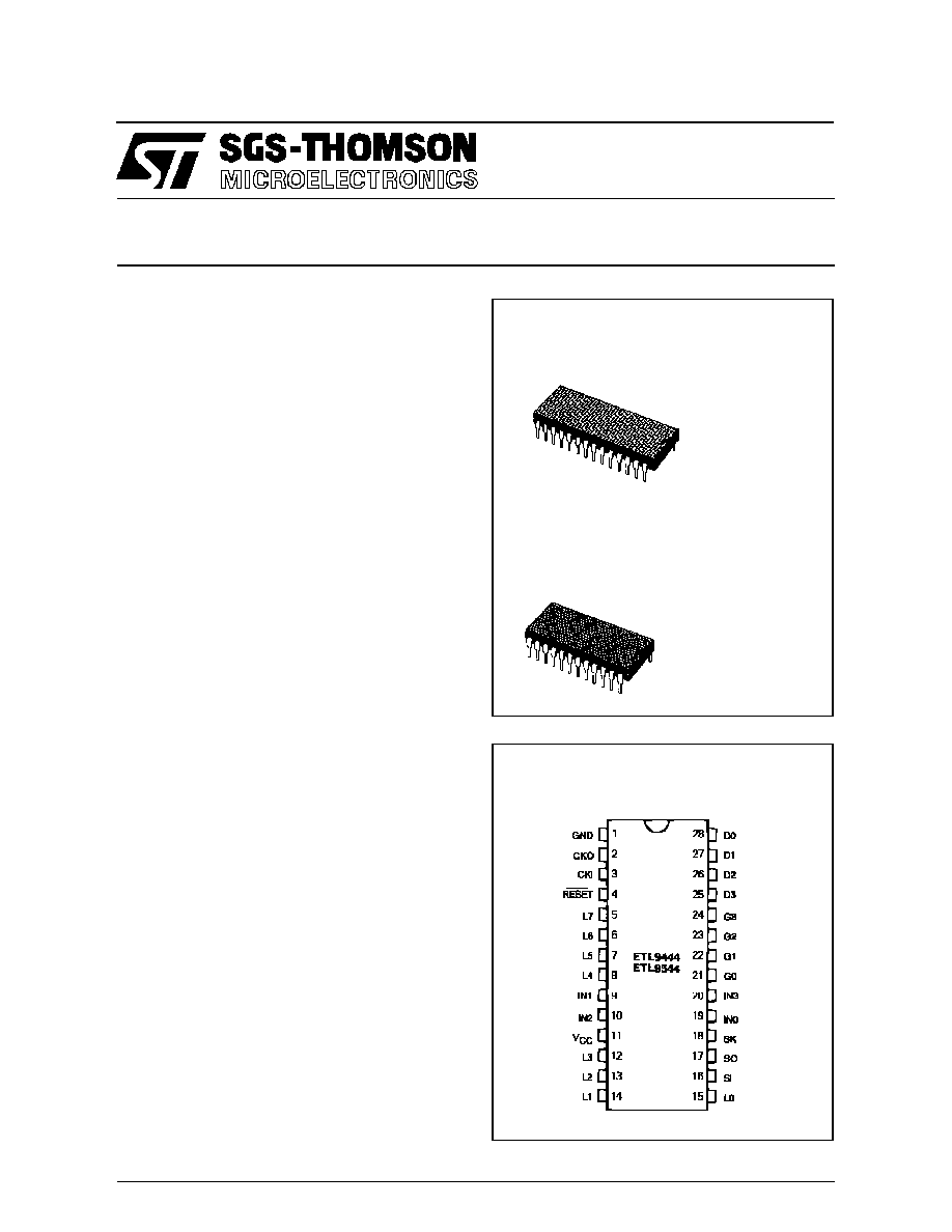
N
(Plastic Package)
DESCRIPTION
The ETL9444/L9445 and ETL9344/L9345 Single-
Chip N-Channel Microcontrollers are fully compati-
ble with the COPS
Æ
family, fabricated using
N-channel, silicon gate XMOS technology. They are
complete microcomputers containing all system ti-
ming, internal logic, ROM, RAM and I/O necessary
to implement dedicated control functions in a variety
of applications. Features include single supply ope-
ration, a variety of output configuration options, with
an instruction set, internal architecture and I/O
scheme designed to facilitate keyboard input, dis-
play output and BCD data manipulation. The
ETL9445 is identical to the ETL9444, except with 19
I/O lines instead of 23 : They are an appropriate
choice for use in numerous human interface control
environments. Standard test procedures and relia-
ble high-density fabrication techniques provide the
medium to large volume customers with a customi-
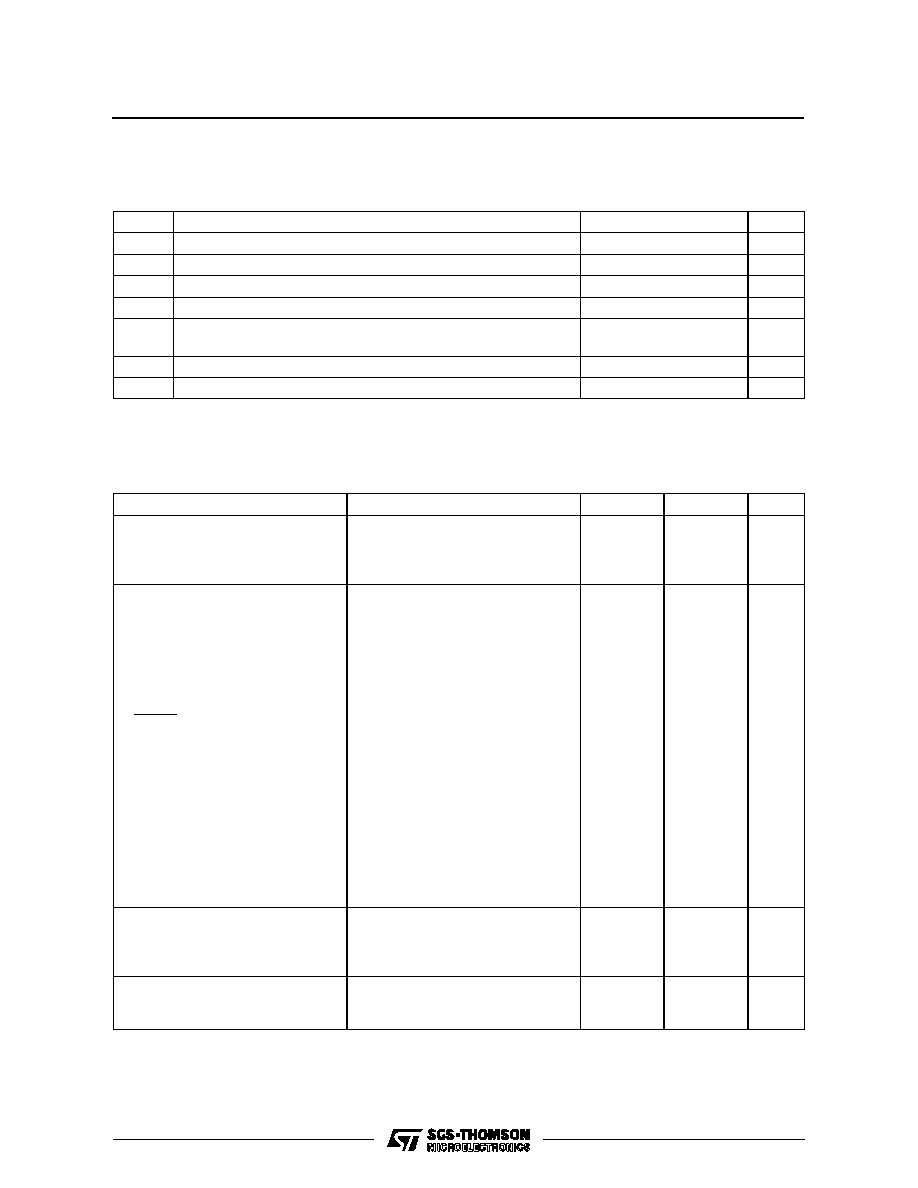
PIN CONNECTION
ETL9345/ETL9345
N
(Plastic Package)
ETL9444/ETL9344
1/27

Figure 1 : Block Diagram (28-pin version).
zed controller oriented processor at a low end-pro-
duct cost.
The ETL9344/L9345 are exact functional equiva-
lents, but extended temperature range versions of
the ETL9444/L9445 respectively.
ETL9444/9445≠ETL9344/9345
2/27
Absolute maximum ratings indicate limits beyond which damage to the device may occur. DC and AC electrical specifications are not en-
sured when operating the device at absolute maximum ratings.
ETL9444/L9445
ABSOLUTE MAXIMUM RATINGS
Symbol
Parameter
Value
Unit
Voltage at any Pin Relative to GND
≠ 0.5 to + 10
V
Ambient Operating Temperature
0 to + 70
∞
C
Ambient Storage Temperature
≠ 65 to + 150
∞
C
Lead Temperature (soldering, 10 seconds)
300
∞
C
Power Dissipation
0.75W at 25
∞
C
0.4W at 70
∞
C
Total Source Current
120
mA
Total Sink Current
120
mA
DC ELECTRICAL CHARACTERISTICS 0
∞
C
T
A
+ 70
∞
C, 4.5V
V
C C
9.5V
(unless otherwise specified)
Parameter
Test Conditions
Mi n.
Max.
Unit
Standard Operating Voltage (V
CC
)
Optional Operating Voltage (V
CC
)
Power Supply Ripple
Operating Supply Current
Note 1
Peak to Peak
All Inputs and Outputs Open
4.5
4.5
6.3
9.5
0.5
13
V
V
V
mA
Input Voltage Levels
CKI Input Levels
Crystal Input (
˜
32,
˜
16,
˜
8)
Logic High (V
IH
)
Logic Low (V
IL
)
Schmitt Trigger Input (
˜
4)
Logic High (V
IH
)
Logic Low (V
IL
)
RESET Input Levels
Logic High
Logic Low
SO Input Level (test mode)
All Other Inputs
Logic High
Logic High
Logic Low
Logic High
Logic Low
Input Capacitance
Hi-Z Input Leakage
Schmitt Trigger Input
V
CC
= Max.
With TTL trip level options
selected, V
CC
= 5V
±
5%.
With high trip level options
selected.
2.0
≠ 0.3
0.7 V
CC
≠ 0.3
0.7 V
CC
≠ 0.3
2.0
3.0
2.0
≠ 0.3
3.6
≠ 0.3
≠ 1
0.4
0.6
0.6
2.5
0.8
1.2
7
+ 1
V
V
V
V
V
V
V
V
V
V
V
V
pF
µ
A
Output Voltage Levels
LSTTL Operation
Logic High (V
O H
)
Logic Low (V
O L
)
V
CC
= 5V
±
5%
I
O H
= ≠ 25
µ
A
I
O L
= 0.36mA
2.7
0.4
V
V
CMOS Operation
Logic High
Logic Low
I
O H
= ≠ 10
µ
A
I
O L
= + 10
µ
A
V
CC
≠ 1
0.2
V
V
Note : 1. V
CC
voltage change must be less than 0.5V in a 1ms period to maintain proper operation.
ETL9444/9445≠ETL9344/9345
3/27
ETL9444/L9445
DC ELECTRICAL CHARACTERISTICS (continued)
Parameter
Test Conditions
Mi n.
Max.
Unit
Output Current Levels
Output Sink Current
SO and SK Outputs (I
O L
)
L
0
-L
7
Outputs and Standard
G
0
-G
3
, D
0
-D
3
Outputs (I
O L
)
G
0
-G
3
and D
0
-D
3
Outputs with
High Current Options (I
O L
)
G
0
-G
3
and D
0
-D
3
Outputs with
Very High Current Options (I
O L
)
CKI (single-pin RC oscillator)
CKO
Output Source Current
Standard Configuration,
All Outputs (I
O H
)
Push-pull Configuration
SO and SK Outputs (I
O H
)
LED Configuration, L
0
-L
7
Outputs, Low Current
Driver Option (I
O H
)
LED Configuration, L
0
-L
7
Outputs, High Current
Driver Option (I
O H
)
TRI-STATE
Æ
Configuration,
L
0
-L
7
Outputs, Low
Current Driver Option (I
O H
)
TRI-STATE
Æ
Configuration,
L
0
-L
7
Outputs, High
Current Driver Option (I
O H
)
Input Load Source Current
V
CC
= 9.5V, V
O L
= 0.4V
V
CC
= 6.3V, V
O L
= 0.4V
V
CC
= 4.5V, V
O L
= 0.4V
V
CC
= 9.5V, V
O L
= 0.4V
V
CC
= 6.3V, V
O L
= 0.4V
V
CC
= 4.5V, V
O L
= 0.4V
V
CC
= 9.5V, V
O L
= 1.0V
V
CC
= 6.3V, V
O L
= 1.0V
V
CC
= 4.5V, V
O L
= 1.0V
V
CC
= 9.5V, V
O L
= 1.0V
V
CC
= 6.3V, V
O L
= 1.0V
V
CC
= 4.5V, V
O L
= 1.0V
V
CC
= 4.5V, V
IH
= 3.5V
V
CC
= 4.5V, V
O L
= 0.4V
V
CC
= 9.5V, V
O H
= 2.0V
V
CC
= 6.3V, V
O H
= 2.0V
V
CC
= 4.5V, V
O H
= 2.0V
V
CC
= 9.5V, V
O H
= 4.75V
V
CC
= 6.3V, V
O H
= 2.4V
V
CC
= 4.5V, V
O H
= 1.0V
V
CC
= 9.5V, V
O H
= 2.0V
V
CC
= 6.0V, V
O H
= 2.0V
V
CC
= 9.5V, V
O H
= 2.0V
V
CC
= 6.0V, V
O H
= 2.0V
V
CC
= 9.5V, V
O H
= 5.5V
V
CC
= 6.3V, V
O H
= 3.2V
V
CC
= 4.5V, V
O H
= 1.5V
V
CC
= 9.5V, V
O H
= 5.5V
V
CC
= 6.3V, V
O H
= 3.2V
V
CC
= 4.5V, V
O H
= 1.5V
V
CC
= 5.0V, V
IL
= 0V
1.8
1.2
0.9
0.8
0.5
0.4
15
11
7.5
30
22
15
2
0.2
≠ 140
≠ 75
≠ 30
≠ 1.4
≠ 1.4
≠ 1.2
≠ 1.5
≠ 1.5
≠ 3.0
≠ 3.0
≠ 0.75
≠ 0.8
≠ 0.9
≠ 1.5
≠ 1.6
≠ 1.8
≠ 10
≠ 800
≠ 480
≠ 250
≠ 18
≠ 13
≠ 35
≠ 25
≠ 140
mA
mA
mA
mA
mA
mA
mA
mA
mA
mA
mA
mA
mA
mA
µ
A
µ
A
µ
A
mA
mA
mA
mA
mA
mA
mA
mA
mA
mA
mA
mA
mA
µ
A
CKO Output
RAM Power Supply Option
Power Requirement
V
R
= 3.3V
6.0
mA
TRI-STATE
Æ
Output Leakage
Current
≠ 2.5
+ 2.5
µ
A
Total Sink Current Allowed
All Outputs Combined
D, G Ports
L
7
-L
4
L
3
-L
0
All Other Pins
Total Source Current Allowed
All I/O Combined
L
7
-L
4
L
3
-L
0
Each L Pin
All Other Pins
120
120
4
4
1.5
120
60
60
30
1.5
mA
mA
mA
mA
mA
mA
mA
mA
mA
mA
ETL9444/9445≠ETL9344/9345
4/27

ETL9344/L9345
ABSOLUTE MAXIMUM RATINGS
Symbol
Parameter
Value
Unit
Voltage at any Pin Relative to GND
≠ 0.5 to + 10
V
Ambient Operating Temperature
≠ 40 to + 85
∞
C
Ambient Storage Temperature
≠ 65 to + 150
∞
C
Lead Temperature (soldering, 10 seconds)
300
∞
C
Power Dissipation
0.75W at 25
∞
C
0.25W at 85
∞
C
Total Source Current
120
mA
Total Sink Current
120
mA
Absolute maximum ratings indicate limits beyond which damage to the device may occur. DC and AC electrical specifications are not en-
sured when operating the device at absolute maximum ratings.
DC ELECTRICAL CHARACTERISTICS ≠ 40
∞
C
T
A
+ 85
∞
C, 4.5V
V
C C
7.5V
(unless otherwise specified)
Parameter
Test Conditions
Mi n.
Max.
Unit
Standard Operating Voltage (V
CC
)
Optional Operating Voltage (V
CC
)
Power Supply Ripple
Operating Supply Current
Note 1
Peak to Peak
All Inputs and Outputs Open
4.5
4.5
5.5
7.5
0.5
15
V
V
V
mA
Input Voltage Levels
CKI Input Levels
Crystal Input
Logic High (V
IH
)
Logic Low (V
IL
)
Schmitt Trigger Input
Logic High (V
IH
)
Logic Low (V
IL
)
RESET Input Levels
Logic High
Logic Low
SO Input Level (test mode)
All Other Inputs
Logic High
Logic High
Logic Low
Logic High
Logic Low
Input Capacitance
Hi-Z Input Leakage
Schmitt Trigger Input
V
CC
= Max.
With TTL trip level options
selected, V
CC
= 5V
±
5%
With high trip level options
selected
2.2
≠ 0.3
0.7 V
CC
≠ 0.3
0.7 V
CC
≠ 0.3
2.2
3.0
2.2
≠ 0.3
3.6
≠ 0.3
≠ 2
0.3
0.4
0.4
2.5
0.6
1.2
7
+ 2
V
V
V
V
V
V
V
V
V
V
V
V
pF
µ
A
Output Voltage Levels
LSTTL Operation
Logic High (V
O H
)
Logic Low (V
O L
)
V
CC
= 5V
±
5%
I
O H
= ≠ 20
µ
A
I
O L
= 0.36mA
2.7
0.4
V
V
CMOS Operation
Logic High
Logic Low
I
O H
= ≠ 10
µ
A
I
O L
= + 10
µ
A
V
CC
≠ 1
0.2
V
V
Note : 1. V
CC
voltage change must be less than 0.5V in a 1ms period to maintain proper operation.
ETL9444/9445≠ETL9344/9345
5/27