
Æ
Monochrome Analog Output CMOS Image Sensors
CD5430F-A
1/33
VV5430
DESCRIPTION
The VV5430 is a highly-integrated VLSI camera device
based on the unique CMOS sensor technology from
STMicroelectronics. It delivers a fully-formatted composite
monochrome video signal. Standards options include EIA
(320 x 244) and CCIR (384 x 287).
It is possible to develop a single chip video camera using this
device that requires only supply voltage in, and delivers
composite video out for connection to a video monitor.
The integrated 75
driver eliminates the need for additional
active components to drive standard loads, including double
terminated lines.
It is also suitable for applications requiring the digitisation of
the video signal or external microprocessor control.
In the VV5430 Frame, Line and Pixel timing signals are
provided to facilitate pixel-locked digitisation of the analog
video data. In addition to the these outputs a synchronisation
input (SIN) is also provided to allow the start of frame to be
synchronised to an external event.
The device features automatic exposure control that allows a
fixed-aperture lens to be used, and incorporates Normal and
Backlit modes to give operation over a wide range of scene
types.
A bi-directional serial interface on the VV5430 allows an
external controller to set operational parameters and control
exposure and gain values directly.
DEVICE FUNCTIONALITY
KEY FEATURES
∑
Complete Video Camera on a single chip
∑
Minimal support circuit
∑
EIA/CCIR standard compatible options
∑
Low power operation - single voltage supply
∑
Integral 75 ohm driver
∑
384 x 287 pixel array
∑
Automatic exposure and gain control
∑
Linear or gamma corrected output option
∑
Automatic black level calibration
∑
Serial Interface Control
∑
Frame and line timing signals for external ADC
APPLICATIONS
∑
Security/Observation systems
∑
Biometric identification
∑
Toys and games
∑
Digital Image capture systems
SPECIFICATIONS
V ID E O
B U F FE R
S A M P LE & H O L D
H O R IZO N TA L S H IFT R E G IS T E R
C O L U M N S E N S E A M P L IF IE R S
V ID E O
A M P
P H O TO D IO D E A R R A Y
A N A L O G
V O LT A G E
R E FS .
D IG ITA L
C O N TR O L
L O G IC .
A GC
A EC
LIN
B K LIT
C C IR
VR T
Vbloom
VOFF
VB G
EB CK
A VO
V E R T IC A L
S H IF T
R E G IS TE R
C KIN
CK OU T
5V
C L O C K
C IR C U IT
IM A G E
C A P TU R E
S E R IA L
I/F
FST
LST
PV
SA B0
SA B1
SD A
SC L
PVB
SIN
C PE
2V7
OD D
EVW T
RESE TB
Pixel resolution
384 x 287 (CCIR)
320 x 243 (EIA)
Array size
4.66mm x 3.54mm
Min. illumination
(min. detectable
signal)
0.5 lux
Exposure control
Automatic (to 146000:1)
Gain control
Automatic (to +20dB)
Signal/Noise ratio
46dB
Supply voltage
5.0v DC
+/-
5%
Supply current
<45mA
Operating
temperature
(ambient)
0
o
C - 40
o
C
(for extended temp. info please
contact STMicroelectronics)
Package type
48LCC

VV5430
CD5430F-A
2/33
Table of Contents
1. Revision History . . . . . . . . . . . . . . . . . . . . . . . . . . . . . . . . . . . . . . . . . . . . . . . . . . . . . . .3
2. Specifications . . . . . . . . . . . . . . . . . . . . . . . . . . . . . . . . . . . . . . . . . . . . . . . . . . . . . . . . .4
2.1 Device Specifications . . . . . . . . . . . . . . . . . . . . . . . . . . . . . . . . . . . . . . . . . . . . . . . . . . . 4
2.2 Defect Specification . . . . . . . . . . . . . . . . . . . . . . . . . . . . . . . . . . . . . . . . . . . . . . . . . . . . 6
3. Device Details . . . . . . . . . . . . . . . . . . . . . . . . . . . . . . . . . . . . . . . . . . . . . . . . . . . . . . . . .7
3.1 Package Details . . . . . . . . . . . . . . . . . . . . . . . . . . . . . . . . . . . . . . . . . . . . . . . . . . . . . . .7
3.2 Pinout Diagram . . . . . . . . . . . . . . . . . . . . . . . . . . . . . . . . . . . . . . . . . . . . . . . . . . . . . . . . 7
3.3 Pin List . . . . . . . . . . . . . . . . . . . . . . . . . . . . . . . . . . . . . . . . . . . . . . . . . . . . . . . . . . . . . .8
4. Video Standards . . . . . . . . . . . . . . . . . . . . . . . . . . . . . . . . . . . . . . . . . . . . . . . . . . . . . .10
4.1 Video Signal Characteristics. . . . . . . . . . . . . . . . . . . . . . . . . . . . . . . . . . . . . . . . . . . . . 10
5. Control Signals for Image Digitisation . . . . . . . . . . . . . . . . . . . . . . . . . . . . . . . . . . . . 13
5.1 Image Capture Control Signal Timing. . . . . . . . . . . . . . . . . . . . . . . . . . . . . . . . . . . . . . 14
6. Shuffle Modes . . . . . . . . . . . . . . . . . . . . . . . . . . . . . . . . . . . . . . . . . . . . . . . . . . . . . . . .15
6.1 Quarter mode output. . . . . . . . . . . . . . . . . . . . . . . . . . . . . . . . . . . . . . . . . . . . . . . . . . . 15
6.2 Quarter mode line timing. . . . . . . . . . . . . . . . . . . . . . . . . . . . . . . . . . . . . . . . . . . . . . . .16
7. Exposure Control. . . . . . . . . . . . . . . . . . . . . . . . . . . . . . . . . . . . . . . . . . . . . . . . . . . . . 18
7.1 Automatic Exposure Control (AEC) . . . . . . . . . . . . . . . . . . . . . . . . . . . . . . . . . . . . . . . 18
7.2 Automatic Gain Control (AGC) . . . . . . . . . . . . . . . . . . . . . . . . . . . . . . . . . . . . . . . . . . . 18
7.3 Backlit Mode . . . . . . . . . . . . . . . . . . . . . . . . . . . . . . . . . . . . . . . . . . . . . . . . . . . . . . . . . 19
8. Serial Communication . . . . . . . . . . . . . . . . . . . . . . . . . . . . . . . . . . . . . . . . . . . . . . . . .20
8.1 Serial Communication Protocol . . . . . . . . . . . . . . . . . . . . . . . . . . . . . . . . . . . . . . . . . .20
9. Read data from camera . . . . . . . . . . . . . . . . . . . . . . . . . . . . . . . . . . . . . . . . . . . . . . . . 22
10. Write to Camera . . . . . . . . . . . . . . . . . . . . . . . . . . . . . . . . . . . . . . . . . . . . . . . . . . . . . 23
10.1 Timing Protocol. . . . . . . . . . . . . . . . . . . . . . . . . . . . . . . . . . . . . . . . . . . . . . . . . . . . . .23
10.2 Header Codes. . . . . . . . . . . . . . . . . . . . . . . . . . . . . . . . . . . . . . . . . . . . . . . . . . . . . . . 24
10.3 Message content . . . . . . . . . . . . . . . . . . . . . . . . . . . . . . . . . . . . . . . . . . . . . . . . . . . . 24
11. Example Support Circuit . . . . . . . . . . . . . . . . . . . . . . . . . . . . . . . . . . . . . . . . . . . . . . 31
12. Ordering Details . . . . . . . . . . . . . . . . . . . . . . . . . . . . . . . . . . . . . . . . . . . . . . . . . . . . . 32

VV5430
Revision History
CD5430F-A
3/33
1.
Revision History
The following is a list of specific changes made to this datasheet since the previous revisions. It does not include general
fomatting changes, but is intended to highlight changes that may affect device operation in a customer system.
Section
Change
2
Removed obsolete test descriptions
Corrected Defect Specification
6
Added reference to generating SIN on only odd or
only evenfields, not both.
10
Setup Code 1: Bit 10 was incorrectly described. This
bit should be set to 0 for normal operation.
Table 1 : Revision History

Specifications
VV5430
CD5430F-A
4/33
2.
Specifications
2.1
Device Specifications
Figure 1 : Spectral Response
The sensor is tested using the example support circuit illustrated later in this document. Standard imaging conditions used for
optical tests employ a tungsten halogen lamp to uniformly illuminate the sensor (to better than 0.5%), or to illuminate specific
areas. A neutral density filter is used to control the level of illumination where required.
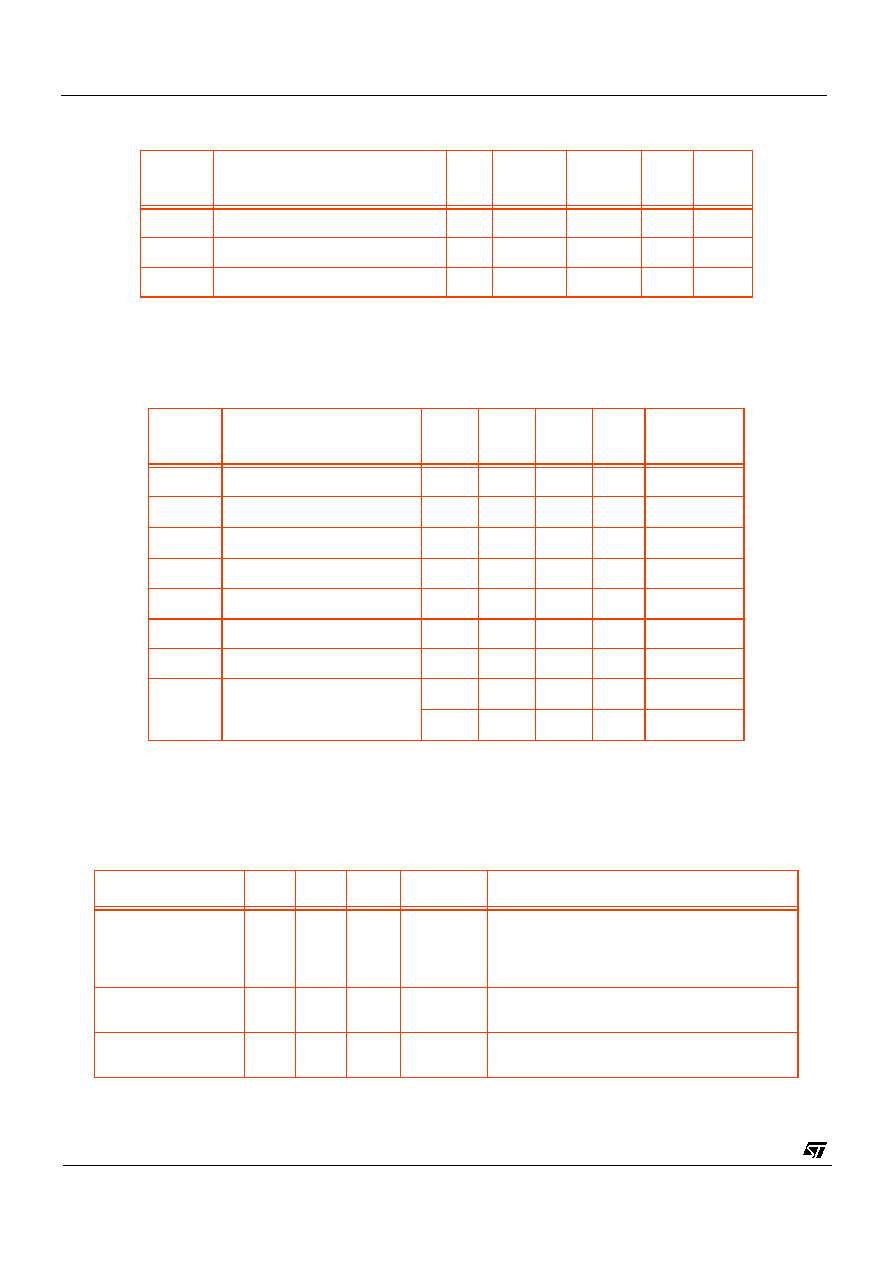
Table 2 : Absolute Maximum Ratings
Note:
Stresses exceeding the Absolute Maximum Ratings may induce failure. Exposure to absolute maximum ratings
for extended periods may reduce reliability. Functionality at or above these conditions is not implied.
Table 3 : DC Operating Conditions
Parameter
Value
Supply Voltage
-0.5 to +7.0 volts
Voltage on other input pins
-0.5 to V
DD
+ 0.5 volts
Ambient Operating Temperature
(contact STMicroelectronics for extended temp. ranges)
0
o
C to 40
o
C
Storage Temperature
-30
o
C to 125
o
C
Maximum DC TTL output Current Magnitude
10mA (per o/p, one at a time, 1sec. duration)
Symbol
Parameter
Min.
Typ.
Max.
Units
Notes
V
DD
Operating supply voltage
4.75
5.0
5.25
Volts
V
IH
Input Voltage Logic "1"
2.4
V
DD
+0.5
Volts
V
IL
Input Voltage Logic "0"
-0.5
0.8
Volts
T
A
Ambient Operating Temperature
0
40
o
C
Still air
Illumination Colour Temp.
3200
o
K
Clock Frequency
Std. CCIR
Exposure
Maximum
Gain
x1
Auto. Gain Control (AGC)
Off
Correction mode
Linear
40
0
50
0
60
0
70
0
80
0
90
0
100
0
11
0
0
1.0
0.8
0.6
0.4
0.2
0
Wavelength nm
No
rma
l
i
s
e
d
Re
sp
o
n
se
VV5430
Specifications
CD5430F-A
5/33
1. Pixel Clock =
CKIN
/
2
2. Serial Interface clock must be generated by host processor.
1. Digital and Analogue outputs unloaded - add output current.
Note:
Devices are normaly not 100% tested for the above characterisation parameters, other than Dark Current Signal.
Table 6 : Operating characteristics
Symbol
Parameter
Min
.
Typ.
Max.
Unit
s
Note
s
CKIN
EIA Crystal frequency
12.0000
MHz
1
CKIN
CCIR Crystal frequency
14.7456
MHz
1
SCL
Serial Data Clock
100
KHz
2
Table 4 : AC Operating Conditions
Symbol
Parameter
Min.
Typ.
Max.
Unit
s
Notes
I
DCC
Digital supply current
10
mA
1
I
ADD
Analog supply current
25
mA
1
I
DD
Overall supply current
35
mA
1
V
REF2V7
Internal voltage reference
2.700
Volts
V
BG
Internal bandgap reference
1.22
Volts
V
OH
Output Voltage Logic "1"
2.4
Volts
I
OH
= 2mA
V
OL
Output Voltage Logic "0"
0.6
Volts
I
OL
= -2mA
I
ILK
Input Leakage current
-1
µ
A
V
IH
on input
1
µ
A
V
IL
on input
Table 5 : Electrical Characteristics
Typical conditions, V
DD
= 5.0 V, T
A
= 27
o
C
Parameter
min.
typ.
max.
units
Note
Dark Current Signal
50
mV/Sec
Modal pixel voltage due to photodiode leakage
under zero illumination with Gain=1
(V
dark
= (V
t1
- V
t2
)/(t1-t2), calculated over two dif-
ferent frames
Sensitivity
6
V/Lux∑Sec
V
Ave
/Lux∑10ms, where Lux gives 50% saturation
with Gain=1 and Exposure=10ms
Min. Illumination
0.5
Lux
Minimum detectable illumination with Standard
CCIR clock