1/11
May 2005
I
HIGH SPEED: t
PD
= 4.4ns (MAX.) at T
A
=85∞C
V
CCB
= 1.65V; V
CCA
= 3.0V
I
LOW POWER DISSIPATION:
I
CCA
= I
CCB
= 5
µ
A(MAX.) at T
A
=85∞C
I
SYMMETRICAL OUTPUT IMPEDANCE:
|I
OHA
| = I
OLA
= 10mA MIN at
V
CCA
= 3.0V; V
CCB
= 1.4V to 3.6V
|I
OHA
| = I
OLA
= 8mA MIN at
V
CCA
= 2.3V; V
CCB
= 1.4 to 3.6V)
I
BALANCED PROPAGATION DELAYS:
t
PLH
t
PHL
I
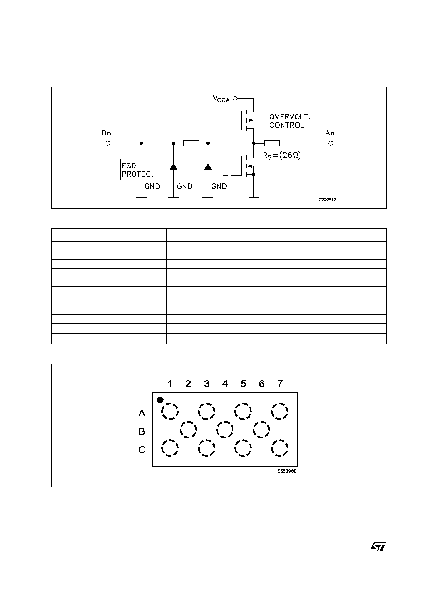
POWER DOWN PROTECTION ON INPUTS
AND OUTPUTS
I
26
SERIES RESISTOR ON A SIDE OUTPUTS
I
OPERATING VOLTAGE RANGE:
V
CCA
(OPR) = 1.4V to 3.6V (1.2V Data Retent)
V
CCB
(OPR) = 1.4V to 3.6V (1.2V Data Retent)
I
MAX DATA RATES:
380 Mbps (1.8V to 3.3V translation)
260 Mbps (<1.8V to 3.3V translation)
260 Mbps (Translate to 2.5V)
210 Mbps (Translate to 1.5V)
100 Mbps (Translate to 1.2V)
I
LATCH-UP PERFORMANCE EXCEEDS
500mA (JESD 17)
I
ESD PERFORMANCE:
HBM > 2000V (MIL STD 883 method 3015);
MM > 200V
I
R
O
HS Compliant for FLIPCHIP Package
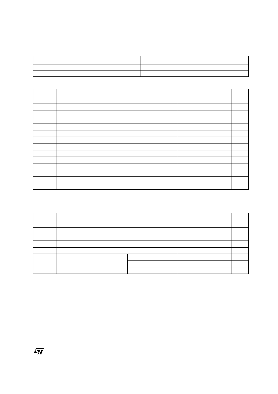
DESCRIPTION
The ST4G3234 is a dual supply low voltage
CMOS 4-BIT BUS BUFFER level translator
fabricated with sub-micron silicon gate and
five-layer metal wiring C
2
MOS technology.
Designed for use as an interface between a 3.3V
bus and a 2.5V or 1.8V bus in a mixed 3.3V/1.8V,
3.3V/2.5V, 1.8V/1.4V and 2.5V/1.8V supply
systems, it achieves high speed operation while
maintaining the CMOS low power dissipation.
This IC is intended for one-way asynchronous
communication between data buses. The input
and output power down protections disable the
device when both power supply are down, so that
the buses are effectively isolated.
The input tolerant buffers allow to translate V
CCB
compatible signals and greater signals than V
CCB
up/down to V
CCA
.
All inputs are equipped with protection circuits
against static discharge, giving them ESD immuni-
ty and transient excess voltage.
ST4G3234
4-BIT DUAL SUPPLY BUS BUFFER LEVEL TRANSLATOR
WITH A SIDE SERIES RESISTOR
Table 1: Order Codes
PACKAGE
T & R
Comments
FLIPCHIP11
ST4G3234BJR
5000 parts per reel
FLIPCHIP
Figure 1: Logic Diagram
Rev. 7
ST4G3234
3/11
Table 3: Truth Table
Table 4: Absolute Maximum Ratings
Absolute Maximum Ratings are those value beyond which damage to the device may occur. Functional operation under these conditions is
not implied
Table 5: Recommended Operating Conditions
1) V
I
from 0.8V to 2.0V at V
CC
= 3.0V
INPUTS Bn (V
CCB
Referred)
OUTPUTS Bn (V
CCA
Referred)
L
L
H
H
Symbol
Parameter
Value
Unit
V
CCA
Output Supply Voltage
-0.5 to +4.6
V
V
CCB
Input Supply Voltage
-0.5 to +4.6
V
V
OA
DC Output Voltage (Power Down Mode: V
CCA
=V
CCB
=Gnd)
-0.5 to +4.6
V
V
IB
DC Input Voltage (Power Down Mode: V
CCA
=V
CCB
=Gnd)
-0.5 to +4.6
V
V
OA
DC Output Voltage
-0.5 to V
CCA
+ 0.5
V
V
IB
DC Input Voltage
-0.5 to +4.6
V
I
IK
DC Input Diode Current
-
20
mA
I
OK
DC Output Diode Current
-
50
mA
I
OA
DC Output Current
±
50
mA
I
CCA
DC V
CCA
or Ground Current
±
100
mA
I
CCB
DC V
CCB
or Ground Current
±
100
mA
P
d
Power Dissipation
400
mW
T
stg
Storage Temperature
-65 to +150
∞C
T
L
Lead Temperature (10 sec)
260
∞C
Symbol
Parameter
Value
Unit
V
CCA
Supply Voltage
1.4 to 3.6
V
V
CCB
Supply Voltage
1.4 to 3.6
V
V
IB
Input Voltage (Bn)
0 to V
CCB
V
V
OA
Output Voltage (An)
0 to V
CCA
V
T
op
Operating Temperature
-40 to 85
∞C
dt/dv
Input Rise and Fall Time (note 1)
V
CCB
= 3.0 to 3.6V
0 to 10
ns/V
V
CCB
= 2.3 to 2.7V
0 to 20
ns/V
V
CCB
= 1.4 to 1.95V
0 to 100
ns/V
ST4G3234
4/11
Table 6: DC Specification
(*) V
CC
range = 3.3±0.3; 2.5±0.2V; 1.8±0.15V
Symbol
Parameter
Test Condition
Value
Unit
V
CCB
(V)(*)
V
CCA
(V)(*)
T
A
= 25 ∞C
-40 to 85 ∞C
Min.
Typ.
Max.
Min.
Max.
V
IHB
High Level Input
Voltage (Bn)
1.4
1.4
to
3.6V
0.65V
CCB
0.65V
CCB
V
1.8
0.65V
CCB
0.65V
CCB
2.5
1.6
1.6
3.3
2.0
2.0
V
ILB
Low Level Input
Voltage (Bn)
1.4
1.4
to
3.6V
0.35V
CCB
0.35V
CCB
V
1.8
0.35V
CCB
0.35V
CCB
2.5
0.7
0.7
3.3
0.8
0.8
V
OHA
High Level
Output Voltage
1.4
to
3.6V
1.4
I
O
=-100
µ
A
1.2
1.2
V
2.75
I
O
=-10mA
2.2
2.2
2.3
I
O
=-8mA
2.0
2.0
1.65
I
O
=-6mA
1.4
1.4
1.4
I
O
=-2mA
1.1
1.1
V
OLA
Low Level
Output Voltage
1.4
to
3.6V
1.4
I
O
=100
µ
A
0.2
0.2
V
2.75
I
O
=10mA
0.55
0.55
2.3
I
O
=8mA
0.30
0.30
1.65
I
O
=6mA
0.25
0.25
1.4
I
O
=2mA
0.20
0.20
I
IB
Input Leakage
Current
2.7
3.6
V
IB
=V
CCB
or GND
±
0.5
±
5
µ
A
1.4
2.7
V
IB
=3.6V or GND
±
0.5
±
5
µ
A
I
OFF
Power Off
Leakage Current
0
0
V
IB
=GND to 3.6V
V
OA
=GND to 3.6V
±
1.0
±
10
µ
A
I
CCtB
Quiescent
Supply Current
1.4
to
3.6V
1.4
to
3.6V
V
IB
=V
CCB
or GND
0.5
5
µ
A
I
CCtA
Quiescent
Supply Current
1.4
to
3.6V
1.4
to
3.6V
V
IB
=V
CCB
or GND
0.5
5
µ
A
I
CCtB
Maximum
Quiescent
Supply Current /
Input (Bn)
2.7
3.6
V
IB
=V
CCB
- 0.6V
V
IB
=V
CCB
or GND
0.75
mA
1.95
3.6
1.95
2.7

ST4G3234
5/11
Table 7: Dynamic Switching Characteristics
Table 8: AC Electrical Characteristics
1) Skew is defined as the absolute value of the difference between the actual propagation delay for any two outputs of the same device switch-
ing in the same direction, either HIGH or LOW (t
OSLH
= | t
PLHm
- t
PLHn
|, t
OSHL
= | t
PHLm
- t
PHLn
|
2) Parameter guaranteed by design
Symbol
Parameter
Test Condition
Value
Unit
V
CCB
(V)
V
CCA
(V)
T
A
= 25 ∞C
-40 to 85 ∞C
Min.
Typ.
Max.
Min.
Max.
V
OLPA
Dynamic Low Level
Quiet An Output
1.4
1.8
C
L
=30pF
V
IL
=0V V
IH
=V
CC
0.2
V
1.4-1.8
2.5
0.25
1.8-2.5
3.3
0.35
V
OLVA
Dynamic Low Level
Quiet An Output
1.4
1.8
C
L
=30pF
V
IL
=0V V
IH
=V
CC
-0.2
V
1.4-1.8
2.5
-0.25
1.8-2.5
3.3
-0.35
V
OHVA
Dynamic High Level
Quiet An Output
1.4
1.8
C
L
=30pF
V
IL
=0V V
IH
=V
CC
1.6
V
1.4-1.8
2.5
2.1
1.8-2.5
3.3
2.7
Symbol
Parameter
Test Condition
Value
Unit
V
CCB
(V)
V
CCA
(V)
-40 to 85 ∞C
Min.
Max.
t
PLH
t
PHL
Propagation Delay Time Bn to An
2.3 to 3.6
1.4
C
L
= 10 pF
2.0
5.5
ns
1.4 to 1.95
1.4
2.0
5.5
2.3 to 3.6
1.65 to 1.95
2.0
5.0
1.4 to 1.95
1.65 to 1.95
2.0
5.2
1.4 to 1.95
2.3 to 2.7
2.0
4.6
1.4 to 1.95
3.0 to 3.6
2.0
4.3
2.3 to 2.7
3.0 to 3.6
1.0
3.5
t
PLH
t
PHL
Propagation Delay Time Bn to An
2.3 to 3.6
1.4
C
L
= 30 pF
R
L
= 500
2.0
7.5
ns
1.4 to 1.95
1.4
2.0
7.9
2.3 to 3.6
1.65 to 1.95
2.0
6.0
1.4 to 1.95
1.65 to 1.95
2.0
6.5
1.4 to 1.95
2.3 to 2.7
2.0
5.7
1.4 to 1.95
3.0 to 3.6
2.0
5.2
2.3 to 2.7
3.0 to 3.6
1.0
4.6
t
OSLH
t
OSHL
Output To Output Skew Time (note1, 2)
1.8
±
0.15
2.5
±
0.2
C
L
= 30 pF
R
L
= 500
0.5
ns
1.8
±
0.15
3.3
±
0.3
0.5
2.5
±
0.2
3.3
±
0.3
0.75