 | –≠–ª–µ–∫—Ç—Ä–æ–Ω–Ω—ã–π –∫–æ–º–ø–æ–Ω–µ–Ω—Ç: FV4N150 | –°–∫–∞—á–∞—Ç—å:  PDF PDF  ZIP ZIP |
1/10
July 2005
STFV4N150
N-CHANNEL 1500V - 5
- 4A TO-220FH
Very High Voltage PowerMESHTM MOSFET
Table 1: General Features
s
TYPICAL R
DS
(on) = 5
s
AVALANCHE RUGGEDNESS
s
GATE CHARGE MINIMIZED
s
VERY LOW INTRINSIC CAPACITANCES
s
HIGH SPEED SWITCHING
s
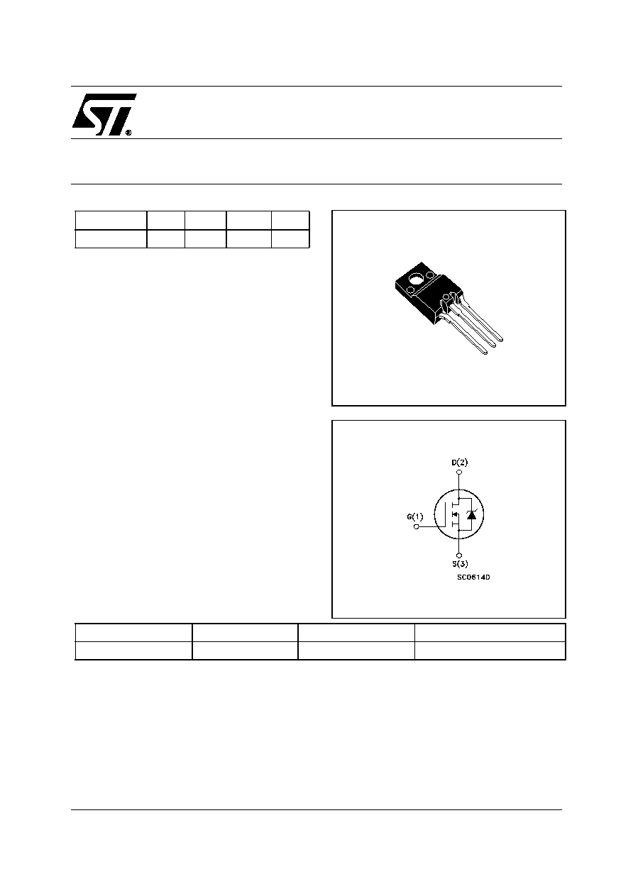
FULLY PLASTIC TO-220 PACKAGE
s
CREEPAGE DISTANCE PATH IS > 4mm
DESCRIPTION
Using the well consolidated high voltage MESH
OVERLAYTM process, STMicroelectronics has de-
signed an advanced family of Power MOSFETs
with outstanding performances. The strengthened
layout coupled with the Company's proprietary
edge termination structure, gives the lowest
RDS(on) per area, unrivalled gate charge and
switching characteristics. The creepage path is
what makes this package unique from TO-220FP.
The creepage distance path between each lead
and between the leads and the heatsink has been
increased to >4.0mm, making this package met all
stringent safety norms in high voltage applications.
APPLICATIONS
s
SWITCH MODE POWER SUPPLIES
Table 2: Order Codes
Figure 1: Package
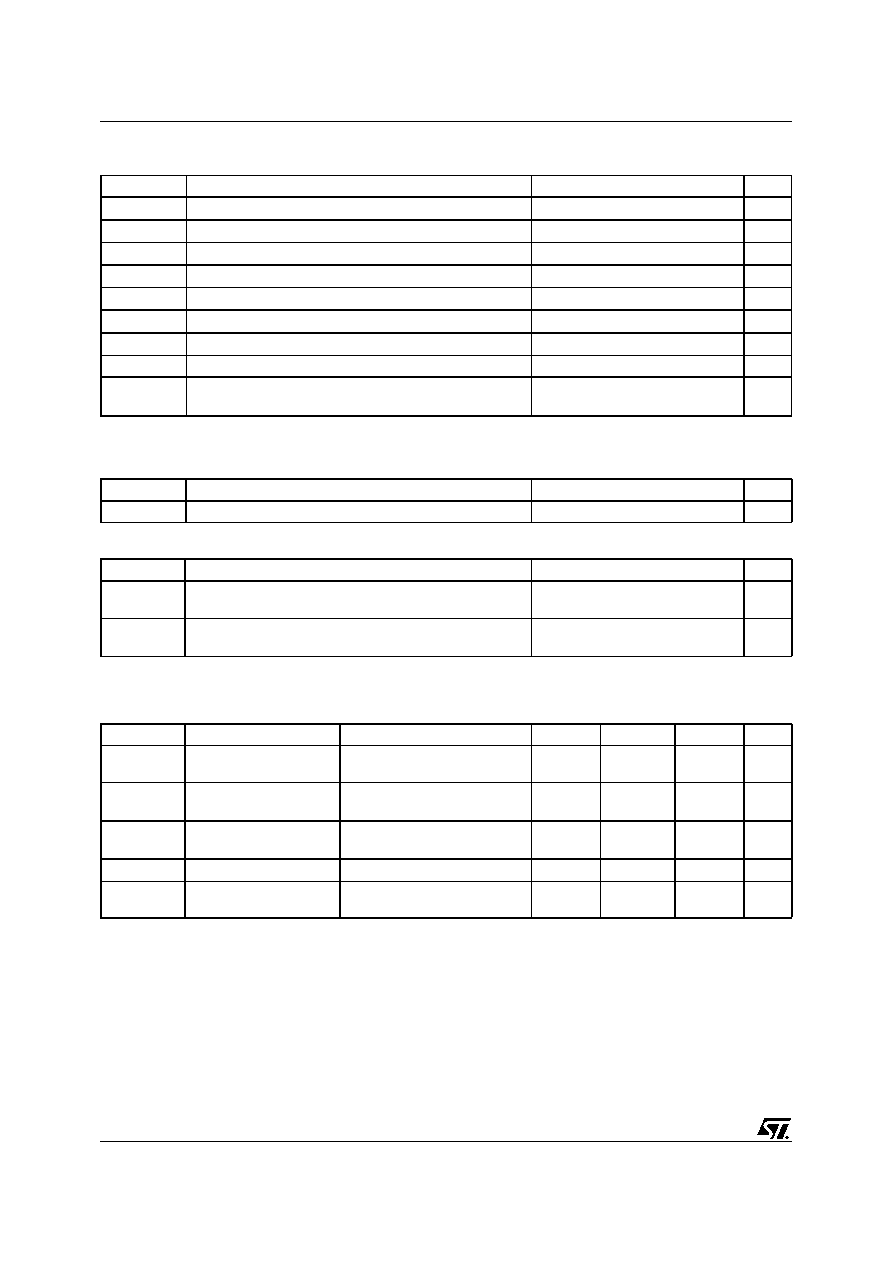
Figure 2: Internal Schematic Diagram
TYPE
V
DSS
R
DS(on)
I
D
Pw
STFV4N150
1500 V
< 7
4 A
40 W
TO-220FH
SALES TYPE
MARKING
PACKAGE
PACKAGING
STFV4N150
FV4N150
TO-220FH
TUBE
Rev. 1
STFV4N150
2/10
Table 3: Absolute Maximum ratings
( ) Pulse width limited by safe operating area
(*) Limited only by maximum temperature allowed
Table 4: Thermal Data
Table 5: Avalanche Characteristics
ELECTRICAL CHARACTERISTICS (T
CASE
=25∞C UNLESS OTHERWISE SPECIFIED)
Table 6: On /Off
Symbol
Parameter
Value
Unit
V
DS
Drain-source Voltage (V
GS
= 0)
1500
V
V
DGR
Drain-gate Voltage (R
GS
= 20 k
)
1500
V
V
GS
Gate- source Voltage
± 30
V
I
D
Drain Current (continuous) at T
C
= 25∞C
4
A
I
D
Drain Current (continuous) at T
C
= 100∞C
2.5
A
I
DM
( )
Drain Current (pulsed)
12
A
P
TOT
Total Dissipation at T
C
= 25∞C
40
W
Derating Factor
0.32
W/∞C
T
j
T
stg
Operating Junction Temperature
Storage Temperature
-55 to 150
∞C
Rthj-case
Thermal Resistance Junction-case Max
3.12
∞C/W
Rthj-amb
Thermal Resistance Junction-ambient Max
62.5
∞C/W
Symbol
Parameter
Max Value
Unit
I
AR
Avalanche Current, Repetitive or Not-Repetitive
(pulse width limited by T
j
max)
4
A
E
AS
Single Pulse Avalanche Energy
(starting T
j
= 25 ∞C, I
D
= I
AR
, V
DD
= 50 V)
350
mJ
Symbol
Parameter
Test Conditions
Min.
Typ.
Max.
Unit
V
(BR)DSS
Drain-source
Breakdown Voltage
I
D
= 1 mA, V
GS
= 0
1500
V
I
DSS
Zero Gate Voltage
Drain Current (V
GS
= 0)
V
DS
= Max Rating
V
DS
= Max Rating,T
C
= 125∞C
10
500
µA
µA
I
GSS
Gate-body Leakage
Current (V
DS
= 0)
V
GS
= ± 30 V
± 100
nA
V
GS(th)
Gate Threshold Voltage
V
DS
= V
GS
, I
D
= 250 µA
3
4
5
V
R
DS(on)
Static Drain-source On
Resistance
V
GS
= 10 V, I
D
= 2 A
5
7
3/10
STFV4N150
ELECTRICAL CHARACTERISTICS (CONTINUED)
Table 7: Dynamic
Table 8: Source Drain Diode
(1) Pulsed: Pulse duration = 300 µs, duty cycle 1.5 %.
(2) Pulse width limited by safe operating area.
Symbol
Parameter
Test Conditions
Min.
Typ.
Max.
Unit
g
fs
(1)
Forward Transconductance
V
DS
= 30 V , I
D
= 2 A
3.5
S
C
iss
C
oss
C
rss
Input Capacitance
Output Capacitance
Reverse Transfer Capacitance
V
DS
= 25 V, f = 1 MHz,
V
GS
= 0
1300
120
12
pF
pF
pF
t
d(on)
t
r
t
d(off)
t
f
Turn-on Delay Time
Rise Time
Turn-off-Delay Time
Fall Time
V
DD
= 750 V, I
D
= 2 A,
R
G
= 4.7
,
V
GS
= 10 V
(see Figure 17)
35
30
45
45
ns
ns
ns
ns
Q
g
Q
gs
Q
gd
Total Gate Charge
Gate-Source Charge
Gate-Drain Charge
V
DD
= 600 V, I
D
= 4 A,
V
GS
= 10 V
(see Figure 20)
30
10
9
50
nC
nC
nC
Symbol
Parameter
Test Conditions
Min.
Typ.
Max.
Unit
I
SD
I
SDM
(2)
Source-drain Current
Source-drain Current (pulsed)
4
12
A
A
V
SD
(1)
Forward On Voltage
I
SD
= 4 A, V
GS
= 0
2
V
t
rr
Q
rr
I
RRM
Reverse Recovery Time
Reverse Recovery Charge
Reverse Recovery Current
I
SD
= 4 A, di/dt = 100 A/µs
V
DD
= 45V
(see Figure 18)
510
3
12
ns
µC
A
t
rr
Q
rr
I
RRM
Reverse Recovery Time
Reverse Recovery Charge
Reverse Recovery Current
I
SD
= 4 A, di/dt = 100 A/µs
V
DD
= 45V, T
j
= 150∞C
(see Figure 18)
650
4
12.6
ns
µC
A
STFV4N150
4/10
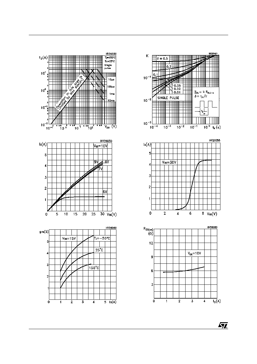
Figure 3: Safe Operating Area
Figure 4: Output Characteristics
Figure 5: Transconductance
Figure 6: Thermal Impedance
Figure 7: Transfer Characteristics
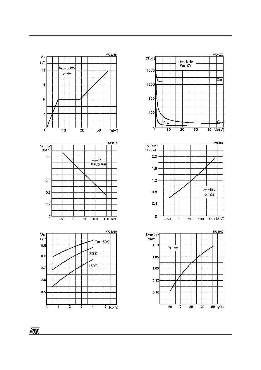
Figure 8: Static Drain-source On Resistance
5/10
STFV4N150
Figure 9: Gate Charge vs Gate-source Voltage
Figure 10: Normalized Gate Thereshold Volt-
age vs Temperature
Figure 11: Source-Drain Diode Forward Char-
acteristics
Figure 12: Capacitance Variations
Figure 13: Normalized On Resistance vs Tem-
perature
Figure 14: Normalized BVdss vs Temperature
STFV4N150
6/10
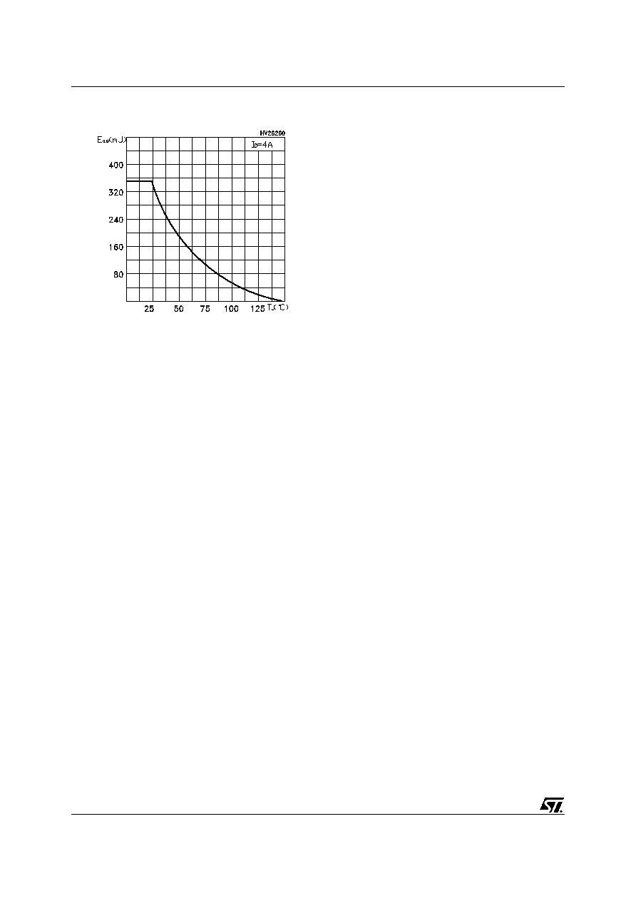
Figure 15: Maximum Avalanche Energy vs
Temperature
7/10
STFV4N150
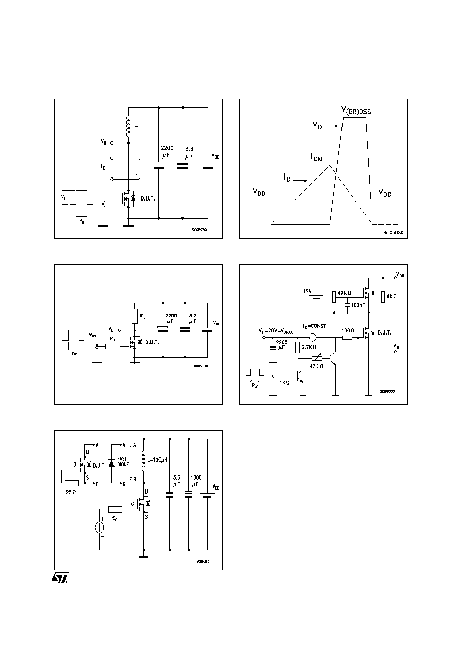
Figure 16: Unclamped Inductive Load Test Cir-
cuit
Figure 17: Switching Times Test Circuit For
Resistive Load
Figure 18: Test Circuit For Inductive Load
Switching and Diode Recovery Times
Figure 19: Unclamped Inductive Waveform
Figure 20: Gate Charge Test Circuit
STFV4N150
8/10
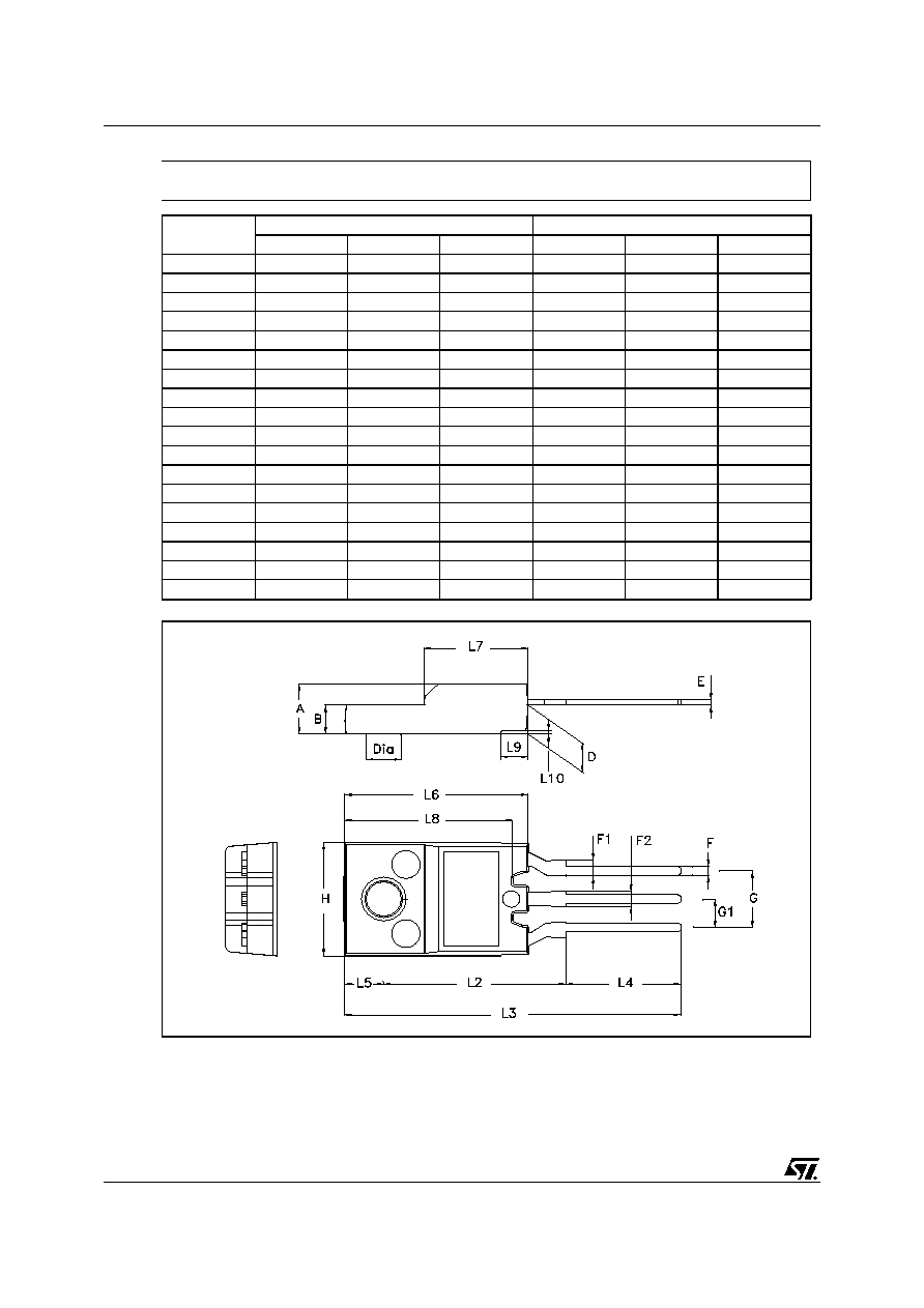
DIM.
mm
inch
MIN.
TYP.
MAX.
MIN.
TYP.
MAX.
A
4.4
4.6
0.173
0.181
B
2.5
2.7
0.098
0.106
D
2.5
2.75
0.098
0.108
E
0.45
0.7
0.017
0.027
F
0.75
1
0.030
0.039
F1
1.3
1.8
0.051
0.070
F2
1.3
1.8
0.051
0.070
G
4.95
5.2
0.195
0.204
G1
2.4
2.7
0.094
0.106
H
10
10.4
0.393
0.409
L2
16
0.630
L3
28.6
30.6
1.126
1.204
L4
9.8
10.6
0.385
0.417
L5
3.4
0.134
L6
15.9
16.4
0.626
0.645
L7
9
9.3
0.354
0.366
L8
14.5
15
0.570
0.590
L9
2.4
0.094
P011W
TO-220FH (Fully plastic High voltage) MECHANICAL DATA
9/10
STFV4N150
Table 9: Revision History
Date
Revision
Description of Changes
07-Jul-2005
1
First release.

STFV4N150
10/10
Information furnished is believed to be accurate and reliable. However, STMicroelectronics assumes no responsibility for the consequences
of use of such information nor for any infringement of patents or other rights of third parties which may result from its use. No license is granted
by implication or otherwise under any patent or patent rights of STMicroelectronics. Specifications mentioned in this publication are subject
to change without notice. This publication supersedes and replaces all information previously supplied. STMicroelectronics products are not
authorized for use as critical components in life support devices or systems without express written approval of STMicroelectronics.
The ST logo is a registered trademark of STMicroelectronics
All other names are the property of their respective owners
© 2005 STMicroelectronics - All Rights Reserved
STMicroelectronics group of companies
Australia - Belgium - Brazil - Canada - China - Czech Republic - Finland - France - Germany - Hong Kong - India - Israel - Italy - Japan -
Malaysia - Malta - Morocco - Singapore - Spain - Sweden - Switzerland - United Kingdom - United States of America