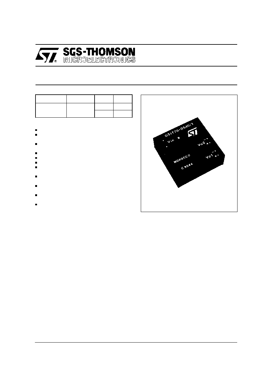
GS1T70-D540/1
ISDN DC-DC CONVERTER
January 1996
1/4
Type
V
i
V
o
I
o
GS1T70-D540/1
25 to 115 V
5 V
90 mA
40 V
10,5 mA
FEATURES
Wide operating line termination voltage
Peak input overvoltage withstand: 1kV for
1.2/50
µ
s
Peak overvoltage withstand on Output 2 (40V):
250V for 10/700
µ
s
Positive or negative input voltage polarity
Input and output filtering
Short-circuit protection on both outputs
Input power during shortcircuit within specifica-
tion
Minimum current drain during stand-by condition:
10
µ
A for Vi<18V
Input-output isolation voltage: 2000V
RMS
for 60
seconds
Output1-output2 isolation voltage: 2000V
RMS
for
60 seconds
Mechanical dimensions (L x W x H): 50.8 mm x
50.8 mm x 18 mm (2" x 2" x 0.71")
DESCRIPTION
The GS1T70-D540/1 converter has been designed
for the "U" interface of an ISDN-NTBA (Network
Termination Basic Access) system with either 4B3T
or 2B1Q standard trasmission.
It meets the requirements of the following specifi-
cations:
EN 60950
CCITT I.430
CCITT G.960
CCITT G.961
ETS 300 002
ETS 300 012
ETS 300 047 (ISDN BASIC ACCESS, Safety and
Protection)
Two isolated outputs, 5V/90mA and 40V/10.5mA
are supplied. The converter offers short-circuit pro-
tection (short-circuit on 40V output doesn't affect
5V output and the input power never exceeds the
limit of the specification), input either voltage polar-
ity, 80% minimum efficiency at maximum load, input
and output filtering to meet very stringent noise
requirements.
The input and the output 2 (40V) stages are pro-
tected against differential overvoltage up to 1kV
(1.2/50
µ
s) and 250V (10/700
µ
s) respectively.
When the input voltage is below 18V, the converter
offers a very high input impedance and a maximum
quiescent current of 10
µ
A.
These features allow the converter to operate di-
rectly connected to the telephone line without any
external components.
In addition, the wide operating input voltage range
allows it to operate within the whole range of LT
(Line Termination) battery voltage and its relevant
line resistance.
2000V
RMS
isolation voltage for 60 second is pro-
vided between input to outputs and between output
1 and output 2.

ELECTRICAL CHARACTERISTICS (T
amb
= 25
∞
C unless otherwise specified)
Std. Conditions:
Line Termination voltage: 47 to 71V Line Resistance (Rs): 10 to 560
87 to 99V 550 to 1400
Symbol
Parameter
Test Conditions
Min
Typ
Max
Unit
Vi
Input Voltage
Std. Conditions
25
115
V
Vipk
Input Transient
Overvoltage
t = 1.2/50
µ
s (pulse)
1
kV
Vist
Start Up Input
Voltage
See fig. 2
28
44
V
Vo1
Output Voltage 1
Std. Conditions
4.75
5
5.25
V
Vo2
Output Voltage 2
Std. Conditions
34
40
42
V
Vor1
Output Ripple
Voltage 1
Std. Conditions
BW = 0 to 20MHz
5
20
mVpp
Vor2
Output Ripple
Voltage 2
Std. Conditions
BW = 0 to 20MHz
10
30
mVpp
eN
Input Noise Voltage
Std. Conditions
BW = 0 to 20MHz
10
30
mVpp
Io1
Output Current 1
Std. Conditions
Io2 = 0 to 10.5 mA Vo1 = 5V
2
90
mA
Io1I
Output Current 1
Limit Initiation
Std. Conditions
Vo1 = 4.75 to 5.25V
110
130
mA
Io2
Output Current 2
Std. Conditions
Io1 = 2 to 90 mA Vo2 = 40V
0
10.5
mA
Iosc2
Output 2 Short
Circuit Current
Std. Conditions
Output Shorted (Indefinite time)
9
14
mA
Vis
Isolation Voltage
(pulse)
Input to Output 1
Input to Output 2
Output 1 to Output 2
2000
VRMS
Top
Operating Ambient
Temperature Range
0
+80
∞
C
Tstg
Storage
Temperature Range
≠ 40
+85
∞
C
2/4
LT (Line Termination Voltage) = 47V to 71V
Rs (Line Resistance) = 10 to 560
LT (Line Termination Voltage) = 87V to 99V
Rs (Line Resistance) = 550 to 1400
Max
Input
Power
(mW)
NT Status
Min
Output
Power 1
(5V)[mW]
Min
Output
Power 2
(40V)[mW]
Max
Input
Power
(mW)
NT Status
Min
Output
Power 1
(5V)[mW]
Min
Output
Power 2
(40V)[mW]
450
Activated
320
0
450
Activated
320
0
950
Activated Emergency
330
410
950
Activated Emergency
330
410
90
Deactivated
25
0
90
Deactived
25
0
180
Deactivated Emergency
25
45
180
Deactivated Emergency
25
45
950
Activated with 40 V
Short circuit
330
Short
circuit
950
Activated with 40V
Short circuit
330
Short
circuit
OUTPUT POWER CHARACTERISTICS
GS1T70-D540/1

3/4
50.8 (2.00)
21.59 (0.85)
19.05 (0.75)
18.0 (0.71)
50.8
(2.00)
1
2
3
4
5
6
5.08 (0.2)
5.08 (0.2)
10.16 (0.4)
10.16 (0.4)
7.62 (0.3)
1.27
(0.05)
Bottom view
3.0 (1.18)
O 1 (0.04)
Package V. Dimensions in mm (inches).
CONNECTION DIAGRAM AND MECHANICAL DATA
Figure 1.
PIN DESCRIPTION
Pin
Description
1
Input (either polarity).
2
Input (either polarity).
3
+5V Output.
4
Return for +5V Output.
5
+40V Output.
6
Return for +40V Output.
GS1T70-D540/1
4/4
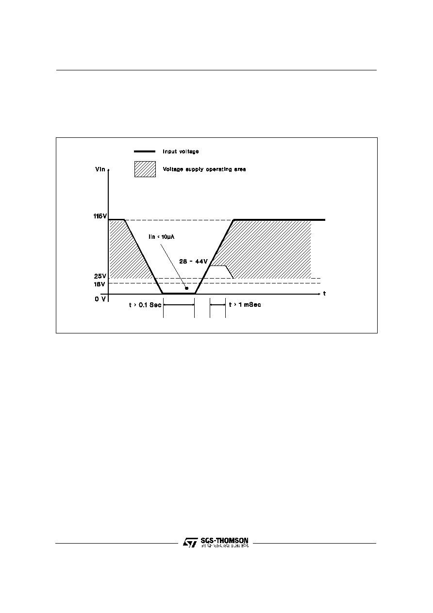
VOLTAGE SUPPLY OPERATING AREA
Figure 2 shows the Voltage Supply Operating area
during a switching OFF-ON sequence.
The start-up voltage is 44V maximum. When the
input voltage is below 18V the maximum quiescent
current is lower than 10
µ
A.
Figure 2.
Information furnished is believed to be accurate and reliable. However, SGS-THOMSON Microelectronics assumes no responsibility for the
consequences of use of such information nor for any infringement of patents or other rights of third parties which may result from its use. No
license is granted by implication or otherwise under any patent or patent rights of SGS-THOMSON Microelectronics. Specification mentioned
in this publication are subject to change without notice. This publication supersedes and replaces all information previously supplied.
SGS-THOMSON Microelectronics products are not authorized for use as critical components in life support devices or systems without express
written approval of SGS-THOMSON Microelectronics.
© 1996 SGS-THOMSON Microelectronics ≠ All Rights Reserved
SGS-THOMSON Microelectronics GROUP OF COMPANIES
Australia - Brazil - China - Canada - France - Germany - Hong Kong - Italy - Japan - Korea - Malaysia - Malta - Morocco - The Netherlands -
Singapore - Spain - Sweden - Switzerland - Taiwan - Thailand - United Kingdom - U.S.A.
GS1T70-D540/1