 | –≠–ª–µ–∫—Ç—Ä–æ–Ω–Ω—ã–π –∫–æ–º–ø–æ–Ω–µ–Ω—Ç: GS5AC-40 | –°–∫–∞—á–∞—Ç—å:  PDF PDF  ZIP ZIP |
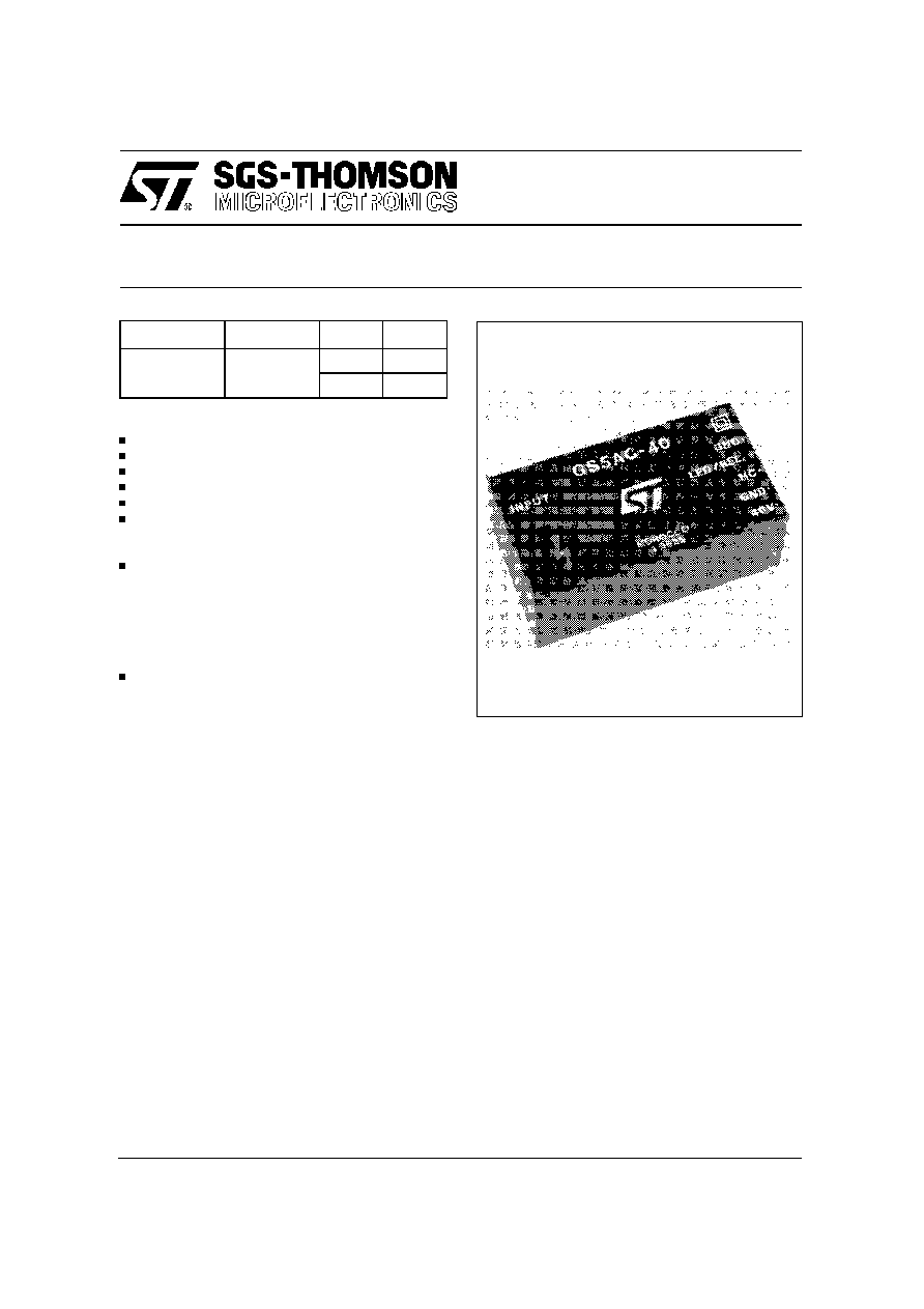
GS5AC-40
ISDN AC-DC CONVERTER
20 January 1997
1/4
PRELIMINARY DATA
Type
V
i
V
o
I
o
GS5AC-40
180 to 264 V
out 1: 40 V 110 mA
out 2: 40 V
10 mA
FEATURES
Large Input voltage range: 180 to 264 V
RMS
Input filter to meet EMI requirements
Peak input overvoltage whitstanding
Input fuse
Input to output insulation
2 insulated outputs:
Vo1 = 35 to 42 V for "S" interface
Vo2 = 36 to 47 V for external relay and LED driver
"S" interface output characteristics:
Peak output of 8 W for 150 ms
Typical output power: 4,5 W
Output filtering to meet ETSI requirements
Hold up time: 20 ms with 4,5 W output power
Continuous short circuit protection
Peak overvoltage withstand: 250 V for 10/700
µ
s
Mechanical dimensions (LxWxH): 80x43x30 mm
DESCRIPTION
The GS5AC-40 converter has been designed for
an ISDN-NTBA (Network Termination Basic Ac-
cess) system with either 4B3T or 2B1Q standard
trasmission.
The converter is able to deliver 40V/110 mA for "S"
interface and is equipped also with a second, aux-
iliary 40V/10 mA output for relay and LED driving.
The converter offers short-circuit protection on both
outputs (short-circuit on 40V output doesn't affect
relay/LED output and the input power never ex-
ceeds the limit of 15 W) and also provides to
remove the auxiliary (relay & LED) output when the
mains is missing, thus allowing the use of a second
"emergency" voltage source (relay contacts are
released). 3000 V
RMS
insulation voltage for 60
seconds is provided between input and the outputs.
Output 1 and Output 2 share the same common
ground (pin 4 is internally connected with pin 6).
The design of the module has been conducted
using, as reference standards, the following:
EN 60950, VDE0878 part 1 class B (EMC),
EN55022 class B (EMC), CCITT 430, ETS 300 012
and ETS 300 047 (ISDN BASIC ACCESS, Safety
and Protection); anyway, please note that no certi-
fication processes have been carried out on the
module itself.
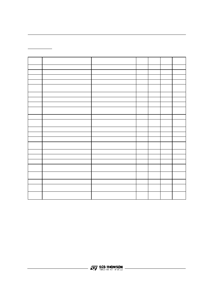
ELECTRICAL CHARACTERISTICS (T
amb
= 25
∞
C unless otherwise specified)
Std. Conditions:
Vin = 180 to 264 V
RMS
Po1 = 0 to 4.5 W
Io2 = 0 to 10 mA
Vo2 = 36 to 47 V
Symbol
Parameter
Test Conditions
Min
Typ
Max
Unit
Vi
Input Voltage
180
264
VRMS
fi
Input Frequency
Vi = 230 VRMS
43
56
Hz
Pi
Input Power
Standard Conditions
7
W
Pi
Input Power
Abnormal Conditions
15
W
Vist
Start up Input Voltage
Output parameters as per
Standard Conditions
100
150
VRMS
Vo1
Output Voltage 1
Standard Conditions
36
38
42
V
Vo2
Output Voltage 2
Standard Conditions
36
38
47
V
Vo2
Output Voltage 2
Emergency Conditions
0
1
V
Vor1
Output Ripple Voltage 1
Standard Conditions
B W: 0 - 20 MHz
100
mVRMS
Io1
Output Current 1
Standard Conditions
0
110
mA
Ioo1
Output Overcurrent
t = 150 ms, Vo1 = 35.5 to 42 V
at Switch-On
180
250
mA
Io1sc
Output 1 short circuit current
10
50
80
mA
Io2
Output current 2
Standard Conditions
0
10
mA
Vo1pf
Power Fail Vo1 threshold
Vo2 fails below 1 V
35.5
36.5
V
Vipf
Power Fail Vi threshold
Output parameters as per
Standard Conditions
150
180
VRMS
Vipk
Input Transient Overvoltage
t = 10/700
µ
s
2.5
kV
Vo1pk
Out 1 Transient Overvoltage
t = 10/700
µ
s
250
V
Vis
Insulation Voltage
Input to outputs, t=60 s
3000
VRMS
Vis
Insulation Voltage (pulse)
Input to outputs,
t = 10/700
µ
s (pulse)
4
kV
th
Hold-up time
Vin = 180 VRMS
Loads as per Std. Conditions
20
ms
MTBF
Mean Time Before Failure
Ground Fixed, MIL-HDBK-217E
1
Mhours
Top
Operating Ambient
Temperature Range
-5
+70
∞
C
Tstg
Storage
Temperature Range
- 40
+85
∞
C
2/4
20 January 1997
GS5AC-40
20 January 1997
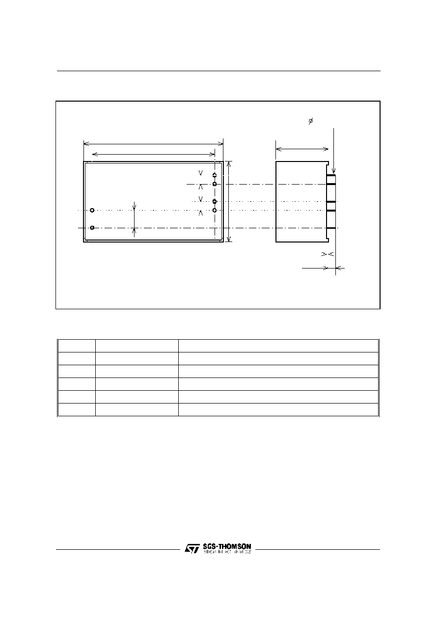
1
2
3
4
43 (1.69)
30 (1.18)
3 (0.12)
Bottom view
10.16 (0.4)
71.12 (2.80)
80 (3.15)
0.6 (0.023)
1 (0.04)
5.08 (0.2)
5.08 (0.2)
10.16 (0.4)
5
6
Figure 1. Connection diagram and mechanical data
3/4
Pin
Function
Description
1
AC Input
Mains input
2
AC Input
Mains input
3
+Vo1
+ 40 V Output for "S" interface
4 & 6
- Vo1 & -Vo2
Output Common Ground
5
+ Vo2
+ External Relay & LED driver
PIN DESCRIPTION
GS5AC-40
4/4
20 January 1997
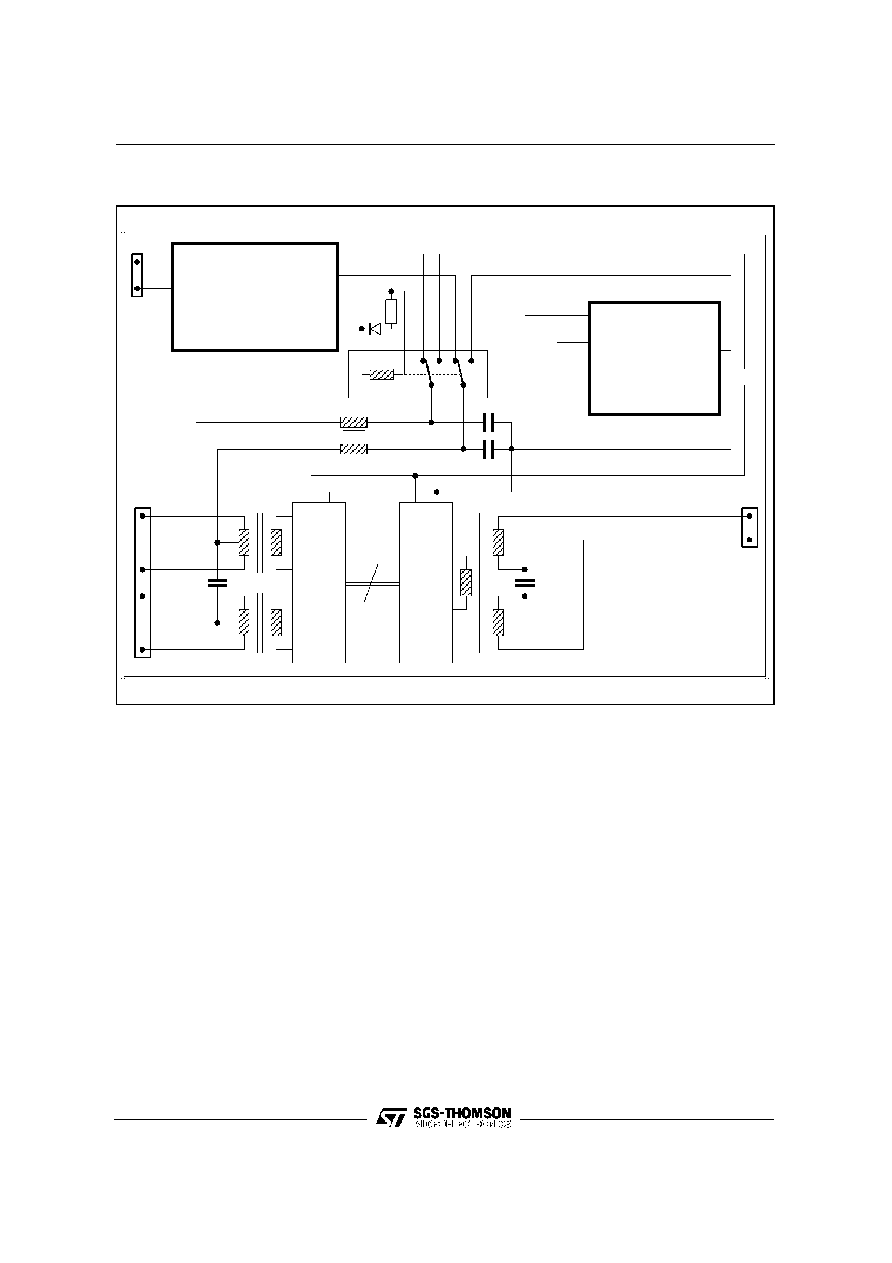
GS1T70-D540/2
40 V
5 V
+
-
+
-
3
4
1
2
"U"
interf.
"S"
interf.
GS5AC-40
1
2
Mains
input
40 V
+
-
Relay/Led
-
+
So
Uo
NT1 board
Relay
5
6
AC/DC converter
DC/DC converter
Led
3
4
5
6
Figure 2. Typical application example
Information furnished is believed to be accurate and reliable. However, SGS-THOMSON Microelectronics assumes no responsibility for the
consequences of use of such information nor for any infringement of patents or other rights of third parties which may result from its use. No
license is granted by implication or otherwise under any patent or patent rights of SGS-THOMSON Microelectronics. Specification mentioned
in this publication are subject to change without notice. This publication supersedes and replaces all information previously supplied.
SGS-THOMSON Microelectronics products are not authorized for use as critical components in life support devices or systems without express
written approval of SGS-THOMSON Microelectronics.
©
1997 SGS-THOMSON Microelectronics ≠ All Rights Reserved
SGS-THOMSON Microelectronics GROUP OF COMPANIES
Australia - Brazil - China - Canada - France - Germany - Hong Kong - Italy - Japan - Korea - Malaysia - Malta - Morocco - The Netherlands -
Singapore - Spain - Sweden - Switzerland - Taiwan - Thailand - United Kingdom - U.S.A.
GS5AC-40