1/14
September 2002
s
SYNCHRONOUS OR ASYNCHRONOUS
PRESET
s
MEDIUM -SPEED OPERATION :
f
CL
=3.6MHz (Typ.) at V
DD
= 10V
s
CASCADABLE
s
QUIESCENT CURRENT SPECIF. UP TO 20V
s
5V, 10V AND 15V PARAMETRIC RATINGS
s
INPUT LEAKAGE CURRENT
I
I
= 100nA (MAX) AT V
DD
= 18V T
A
= 25įC
s
100% TESTED FOR QUIESCENT CURRENT
s
MEETS ALL REQUIREMENTS OF JEDEC
JESD13B "STANDARD SPECIFICATIONS
FOR DESCRIPTION OF B SERIES CMOS
DEVICES"
DESCRIPTION
HCF40102B is a monolithic integrated circuit
fabricated in Metal Oxide Semiconductor
technology available in DIP and SOP packages.
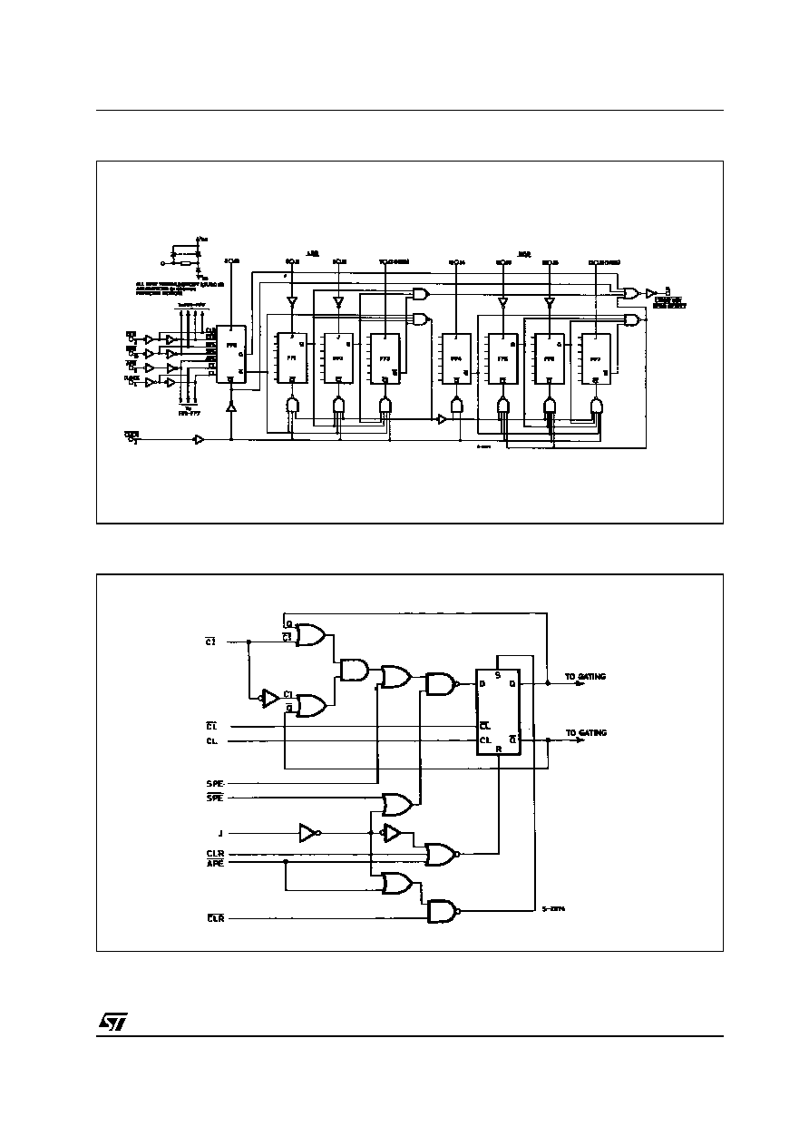
HCF40102B consists of an 8-stage synchronous
down counter with a single output that is active
when the internal count is zero. This device is
configured as two cascaded 4-bit BCD counters. It
has control inputs for enabling or disabling the
clock, for clearing the counter to its maximum
count, and for presetting the counter either
synchronously or asynchronously. All control
inputs and the CARRY-OUT/ZERO DETECT
output are active-low logics. In normal operation,
the counter is decremented by one count on each
positive transition of the CLOCK. Counting is
inhibited when the CARRY-IN/COUNTER
ENABLE (CI/CE) input is high. The CARRY-OUT/
ZERO DETECT (CO/ZD) output goes low when
the count reaches zero if the CI/CE input is low,
and remains low for one full clock period. When
the SYNCHRONOUS PRESET ENABLE (SPE)
input is low, data at the JAM input is clocked into
the counter on the next positive clock transition
regardless of the state of the CI/CE input. When
the ASYNCHRONOUS PRESET ENABLE (APE)
input is low, data at the JAM inputs is
asynchronously forced into the counter regardless
of the state of the SPE, CI/CE, or CLOCK inputs.
JAM inputs J0-J7 represent two 4-bit BCD words.
When the CLEAR (CLR) input is low, the counter
is asynchronously cleared to its maximum count
(99
10
) regardless of the state of any other input.
The precedence relationship between control
input is indicated in the truth table. If all control
HCF40102B
8-STAGE PRESETTABLE SYNCHRONOUS
2 DECADE BCD DOWN COUNTERS
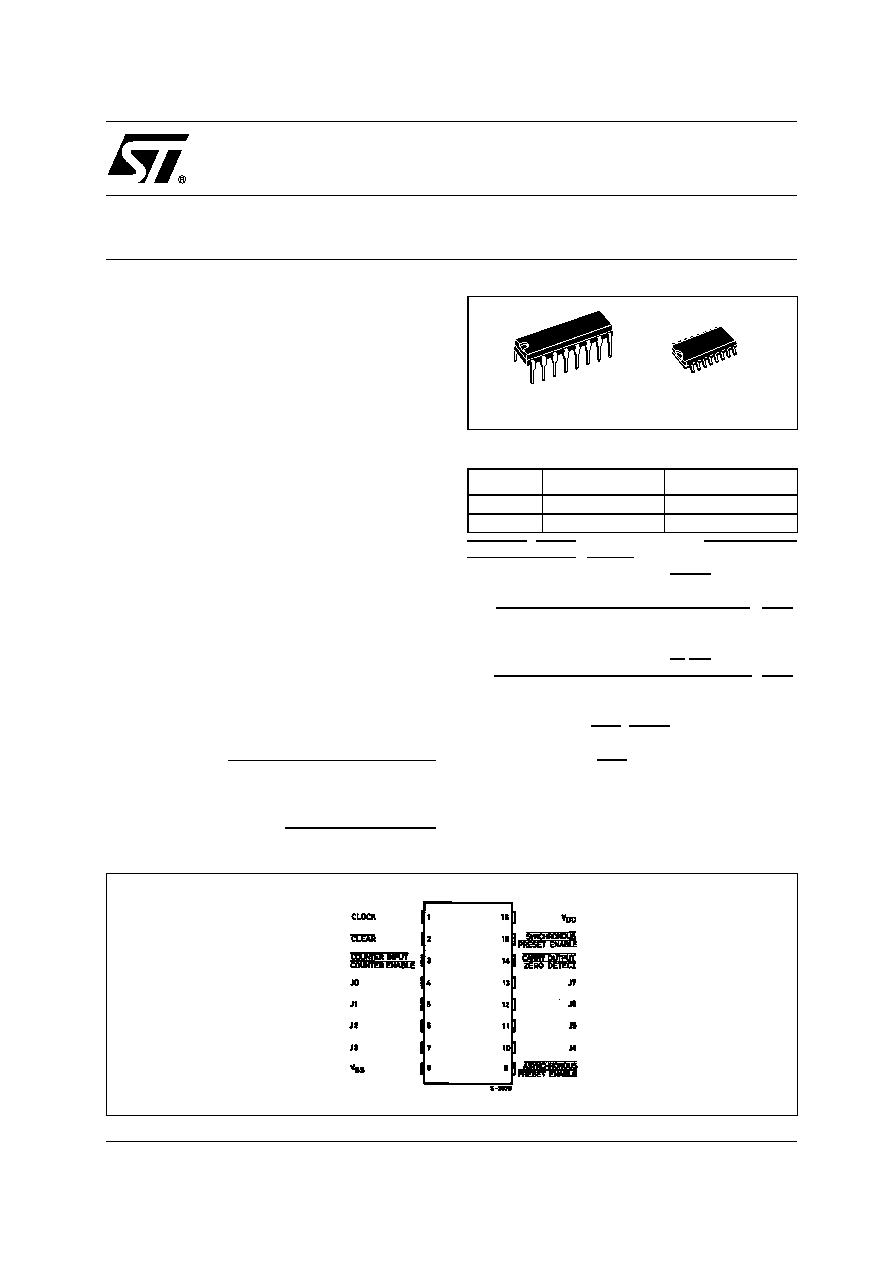
PIN CONNECTION
ORDER CODES
PACKAGE
TUBE
T & R
DIP
HCF40102BEY
SOP
HCF40102BM1
HCF40102M013TR
DIP
SOP
HCF40102B
2/14
inputs are high at the time of zero count, the
counters will jump to the maximum count, giving a
counting sequence of 100 clock pulses long.
HCF40102B may be cascaded using the CI/CE
input and the CO/ZD output, in either a
synchronous or ripple mode.
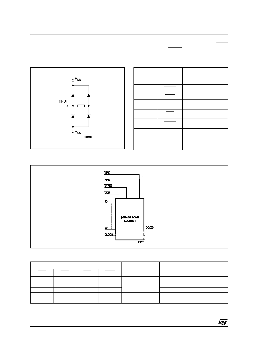
INPUT EQUIVALENT CIRCUIT
PIN DESCRIPTION
FUNCTIONAL DIAGRAM
TRUTH TABLE
X : Don't Care
Clock connected to Clock input
Synchronous Operation : changes occur on negative to positive clock transitions.
PIN No
SYMBOL
NAME AND FUNCTION
1
CLOCK
Clock Input (LOW to
HIGH edge triggered)
2
CLEAR
Asynchronous Master
Reset Input (Active Low)
3
CI/CE
Terminal Enable Input
4, 5, 6, 7, 10,
11, 12, 13
J0 to J7
Jam Inputs
9
APE
Asynchronous Preset
Enable Inputs(Active Low)
14
CO/ZD
Terminal Count Output
(Active Low)
15
SPE
Synchronous Preset
Enable Input (Active Low)
8
V
SS
Negative Supply Voltage
16
V
DD
Positive Supply Voltage
CONTROL INPUTS
PRESET MODE
ACTION
CLR
APE
SPE
CI/CE
H
H
H
H
Synchronous
Inhibit Counter
H
H
H
L
Count Down
H
H
L
X
Preset on Next Positive Clock Transition
H
L
X
X
Asynchronous
Preset Asynchronously
L
X
X
X
Clear to Maximum Count
HCF40102B
4/14
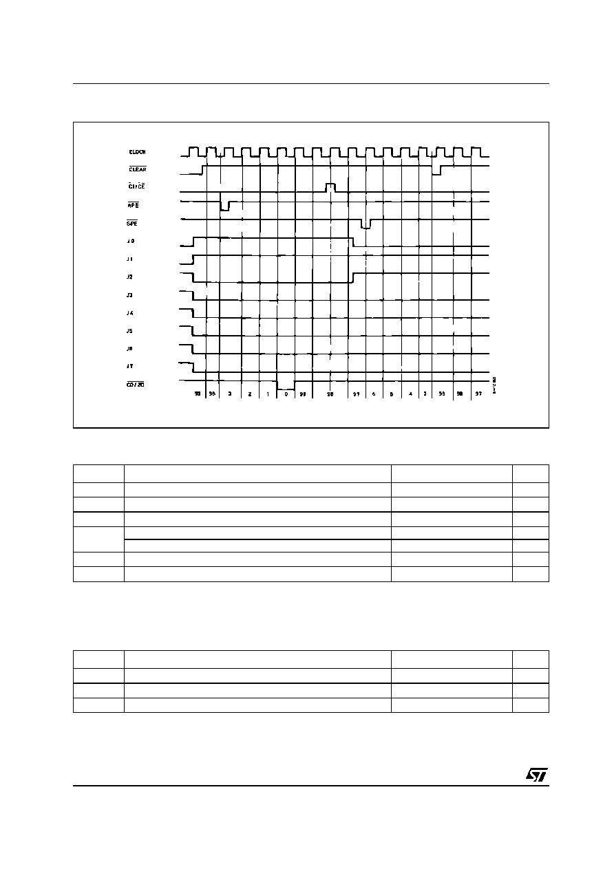
TIMING CHART
ABSOLUTE MAXIMUM RATINGS
Absolute Maximum Ratings are those values beyond which damage to the device may occur. Functional operation under these conditions is
not implied.
All voltage values are referred to V
SS
pin voltage.
RECOMMENDED OPERATING CONDITIONS
Symbol
Parameter
Value
Unit
V
DD
Supply Voltage
-0.5 to +22
V
V
I
DC Input Voltage
-0.5 to V
DD
+ 0.5
V
I
I
DC Input Current
Ī
10
mA
P
D
Power Dissipation per Package
200
mW
Power Dissipation per Output Transistor
100
mW
T
op
Operating Temperature
-55 to +125
įC
T
stg
Storage Temperature
-65 to +150
įC
Symbol
Parameter
Value
Unit
V
DD
Supply Voltage
3 to 20
V
V
I
Input Voltage
0 to V
DD
V
T
op
Operating Temperature
-55 to 125
įC