
1/11
September 2002
s
ONE INPUT AND TWO OUTPUT BUSES
s
UNLIMITED EXPANSION IN BIT AND WORD
DIRECTION
s
DATA LINES HAVE LATCHED INPUTS
s
3-STATE OUTPUTS
s
SEPARATE CONTROL OF EACH BUS,
ALLOWING SIMULTANEOUS
INDEPENDENT READING AND ANY OF
FOUR REGISTERS ON BUS A AND BUS B
AND INDEPENDENT WRITING INTO ANY
OF THE FOUR REGISTERS
s
40108B IS PIN-COMPATIBLE WITH
INDUSTRY TYPE MC14580
s
STANDARDIZED, SYMMETRICAL OUTPUT
CHARACTERISTICS
s
QUIESCENT CURRENT SPECIF. UP TO 20V
s
5V, 10V AND 15V PARAMETRIC RATINGS
s
INPUT LEAKAGE CURRENT
I
I
= 100nA (MAX) AT V
DD
= 18V T
A
= 25∞C
s
100% TESTED FOR QUIESCENT CURRENT
s
MEETS ALL REQUIREMENTS OF JEDEC
JESD13B "STANDARD SPECIFICATIONS
FOR DESCRIPTION OF B SERIES CMOS
DEVICES"
DESCRIPTION
HCF40108B is a monolithic integrated circuit
fabricated in Metal Oxide Semiconductor
technology available in SOP packages.
HCF40108B is a 4 x 4 multiport register containing
four 4-bit registers, a write address decoder, two
separate read address decoders, and two 3-state
output buses. When the ENABLE input is low, the
corresponding output bus is switched,
independently of the clock, to a high impedance
state. The high impedance third state provides the
outputs with the capability of being connected to
the bus lines in a bus organized system without
the need for interface or pull-up components.
When the WRITE ENABLE input is high, all data
input lines are latched on the positive transition of
the CLOCK and the data is entered into the word
selected by the write address lines. When WRITE
ENABLE is low, the CLOCK is inhibited and no
new data is entered. In either case, the contents of
any word may be accessed via the read address
lines independent of the state of the CLOCK input.
HCF40108B
4 x 4 MULTIPORT REGISTER
PIN CONNECTION
ORDER CODES
PACKAGE
TUBE
T & R
SOP
HCF40108BM1
HCF40108M013TR
SOP
HCF40108B
2/11
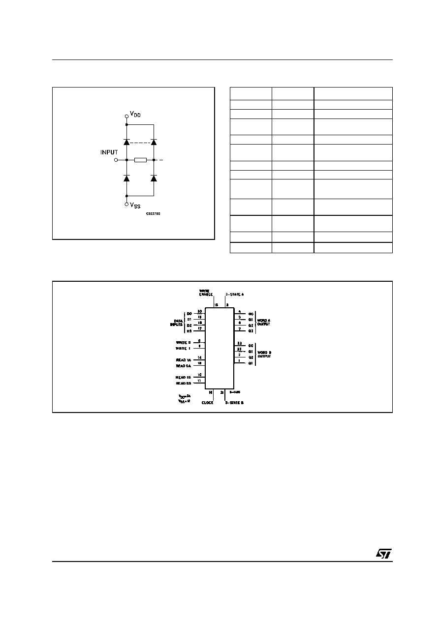
IINPUT EQUIVALENT CIRCUIT
PIN DESCRIPTION
FUNCTIONAL DIAGRAM
PIN No
SYMBOL
NAME AND FUNCTION
4, 5, 6, 7
Q0A to Q3A Word A Output
22, 23, 2, 1
Q0B to Q3B Word B Output
20, 19, 18,
17
D0 to D3
Data Inputs
16
CLOCK
Clock Input
15
WRITE
ENABLE
Write Enable Input
21
3-STATE B
3 State Output
3
3-STATE A
3 State Output
8, 9
WRITE 0,
WRITE 1
Write Address Inputs
10, 11
READ 0B,
READ 1B
Read Address Inputs
13, 14
READ 0A,
READ 1A
Read Address Inputs
12
V
SS
Negative Supply Voltage
24
V
DD
Positive Supply Voltage

HCF40108B
3/11
LOGIC DIAGRAM

HCF40108B
4/11
SCHEMATIC DIAGRAM
HCF40108B
5/11
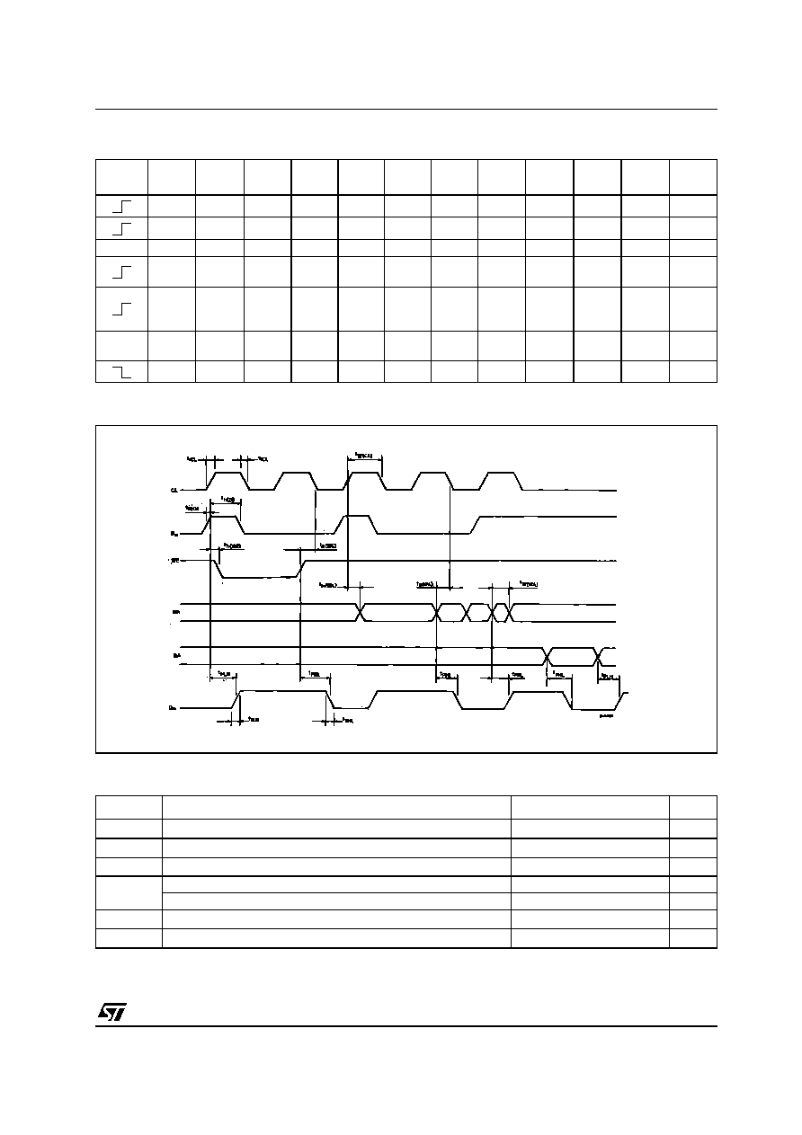
TRUTH TABLE
TIMING CHART
ABSOLUTE MAXIMUM RATINGS
Absolute Maximum Ratings are those values beyond which damage to the device may occur. Functional operation under these conditions is
not implied.
All voltage values are referred to V
SS
pin voltage.
CLOCK
Write
Enable
Write 1 Write 2
Read
1A
Read
0A
Read
1B
Read
0B
Enable
A
Enable
B
Dn
DnA
QnB
H
S1
S2
S1
S2
S1
S2
H
H
H
H
H
H
S1
S2
S1
S2
S1
S2
H
L
L
L
L
X
X
X
X
X
X
X
X
L
L
Z
Z
Z
H
L
L
L
H
H
L
H
H
Dn to
word 0
Word 1
Out
Word 2
Out
L
L
L
L
H
H
L
H
H
Word 0
not
altered
Word 1
Out
Word 2
Out
X
X
X
X
H
L
L
H
H
X
X
Word 2
Out
Word 1
Out
X
X
X
X
X
X
X
H
H
X
NC
NC
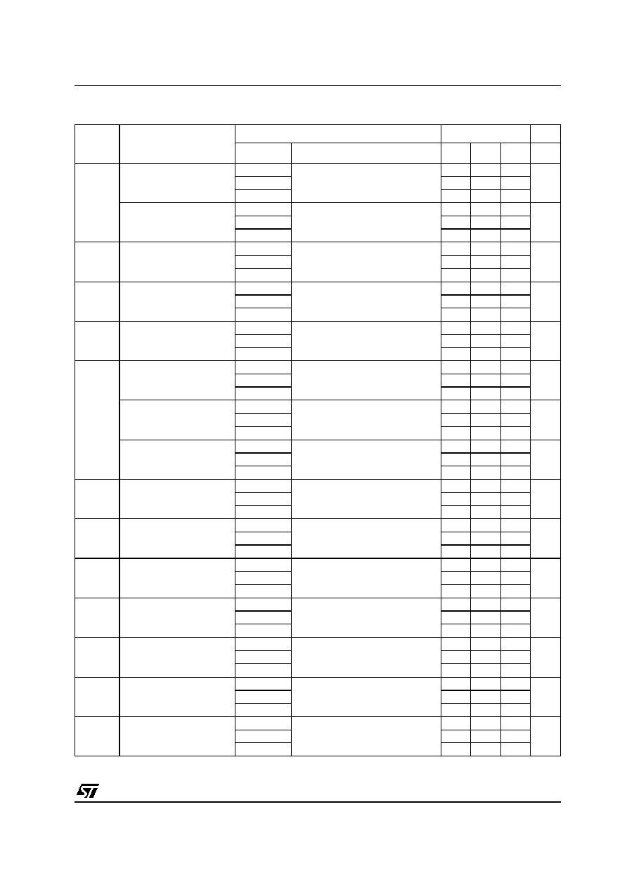
Symbol
Parameter
Value
Unit
V
DD
Supply Voltage
-0.5 to +22
V
V
I
DC Input Voltage
-0.5 to V
DD
+ 0.5
V
I
I
DC Input Current
±
10
mA
P
D
Power Dissipation per Package
200
mW
Power Dissipation per Output Transistor
100
mW
T
op
Operating Temperature
-55 to +125
∞C
T
stg
Storage Temperature
-65 to +150
∞C

HCF40108B
6/11
RECOMMENDED OPERATING CONDITIONS
DC SPECIFICATIONS
The Noise Margin for both "1" and "0" level is: 1V min. with V
DD
=5V, 2V min. with V
DD
=10V, 2.5V min. with V
DD
=15V
Symbol
Parameter
Value
Unit
V
DD
Supply Voltage
3 to 20
V
V
I
Input Voltage
0 to V
DD
V
T
op
Operating Temperature
-55 to 125
∞C
Symbol
Parameter
Test Condition
Value
Unit
V
I
(V)
V
O
(V)
|I
O
|
(
µ
A)
V
DD
(V)
T
A
= 25∞C
-40 to 85∞C
-55 to 125∞C
Min.
Typ.
Max.
Min.
Max.
Min.
Max.
I
L
Quiescent Current
0/5
5
0.04
5
150
150
µ
A
0/10
10
0.04
10
300
300
0/15
15
0.04
20
600
600
0/20
20
0.08
100
3000
3000
V
OH
High Level Output
Voltage
0/5
<1
5
4.95
4.95
4.95
V
0/10
<1
10
9.95
9.95
9.95
0/15
<1
15
14.95
14.95
14.95
V
OL
Low Level Output
Voltage
5/0
<1
5
0.05
0.05
0.05
V
10/0
<1
10
0.05
0.05
0.05
15/0
<1
15
0.05
0.05
0.05
V
IH
High Level Input
Voltage
0.5/4.5
<1
5
3.5
3.5
3.5
V
1/9
<1
10
7
7
7
1.5/13.5
<1
15
11
11
11
V
IL
Low Level Input
Voltage
4.5/0.5
<1
5
1.5
1.5
1.5
V
9/1
<1
10
3
3
3
13.5/1.5
<1
15
4
4
4
I
OH
Output Drive
Current
0/5
2.5
<1
5
-1.36
-3.2
-1.1
-1.1
mA
0/5
4.6
<1
5
-0.44
-1
-0.36
-0.36
0/10
9.5
<1
10
-1.1
-2.6
-0.9
-0.9
0/15
13.5
<1
15
-3.0
-6.8
-2.4
-2.4
I
OL
Output Sink
Current
0/5
0.4
<1
5
0.44
1
0.36
0.36
mA
0/10
0.5
<1
10
1.1
2.6
0.9
0.9
0/15
1.5
<1
15
3.0
6.8
2.4
2.4
I
I
Input Leakage
Current
0/18
Any Input
18
±
10
-5
±
0.1
±
1
±
1
µ
A
I
OZ
3-State Output
Leakage Current
0/18
Any Input
18
±
10
-4
±
0.4
±
12
±
12
µ
A
C
I
Input Capacitance
Any Input
5
7.5
pF
HCF40108B
7/11
DYNAMIC ELECTRICAL CHARACTERISTICS (T
amb
= 25∞C, C
L
= 50pF, R
L
= 200K
, t
r
= t
f
= 20 ns)
Symbol
Parameter
Test Condition
Value (*)
Unit
V
DD
(V)
Min.
Typ.
Max.
t
PHL
t
PLH
Propagation Delay Time
Clock or Write Enable to Q
5
360
720
ns
10
140
280
15
100
200
Propagation Delay Time
Read or Write Address to
Q
5
300
600
ns
10
120
240
15
85
170
t
PZH
t
PHZ
3-State Disable Delay
Time
5
100
200
ns
10
50
100
15
40
80
t
PZL
t
PLZ
3-State Display Delay Time
5
130
260
ns
10
60
120
15
50
100
t
THL
t
TLH
Output Transition Time
5
100
200
ns
10
50
100
15
40
80
t
setup
Setup Time Data to Clock
t
s(D)
5
0
-95
ns
10
0
-35
15
0
-20
Setup Time Write Enable
to Clock t
s(WE)
5
250
125
ns
10
100
50
15
70
35
Setup Time Write Address
to Clock t
s(WA)
5
250
125
ns
10
100
50
15
70
35
t
r,
t
s
Clock Rise and Fall Time
5
15
ns
10
5
15
5
t
hold
Hold Time Data to Clock
t
s(D)
5
220
110
ns
10
100
50
15
80
40
Hold Time Write Enable to
Clock t
s(WE)
5
270
135
ns
10
130
65
15
80
40
Hold Time Write Address
to Clock t
s(WA)
5
330
165
ns
10
140
70
15
90
45
t
W
Clock Pulse Width
Clock or Write Enable
t
W(CL)
5
350
175
ns
10
130
65
15
90
45
t
W
Clock Pulse Width
Write Address t
W(WA)
5
300
150
ns
10
150
75
15
90
45
f
CL
Maximum Clock Input
Frequency
5
1.5
3
MHz
10
3.5
7
15
4.5
9

HCF40108B
8/11
TEST CIRCUIT
C
L
= 50pF or equivalent (includes jig and probe capacitance)
R
L
= 200K
R
T
= Z
OUT
of pulse generator (typically 50
)
WAVEFORM : ENABLE AND DISABLE TIME
TEST
SWITCH
t
PLH
, t
PHL
Open
t
PZL
, t
PLZ
V
DD
t
PZH
, t
PHZ
V
SS

HCF40108B
9/11
SWITCHING WAVEFORM

HCF40108B
10/11
DIM.
mm.
inch
MIN.
TYP
MAX.
MIN.
TYP.
MAX.
A
2.65
0.104
a1
0.1
0.2
0.004
0.008
a2
2.45
0.096
b
0.35
0.49
0.014
0.019
b1
0.23
0.32
0.009
0.012
C
0.5
0.020
c1
45∞ (typ.)
D
15.20
15.60
0.598
0.614
E
10.00
10.65
0.393
0.419
e
1.27
0.050
e3
13.97
0.550
F
7.40
7.60
0.291
0.300
L
0.50
1.27
0.020
0.050
S
∞ (max.)
SO-24 MECHANICAL DATA
PO13T
F
C
L
E
a1
b1
A
e
D
e3
b
24
13
1
1
2
c1
s
a2
8

HCF40108B
11/11
Information furnished is believed to be accurate and reliable. However, STMicroelectronics assumes no responsibility for the
consequences of use of such information nor for any infringement of patents or other rights of third parties which may result from
its use. No license is granted by implication or otherwise under any patent or patent rights of STMicroelectronics. Specifications
mentioned in this publication are subject to change without notice. This publication supersedes and replaces all information
previously supplied. STMicroelectronics products are not authorized for use as critical components in life support devices or
systems without express written approval of STMicroelectronics.
© The ST logo is a registered trademark of STMicroelectronics
© 2002 STMicroelectronics - Printed in Italy - All Rights Reserved
STMicroelectronics GROUP OF COMPANIES
Australia - Brazil - Canada - China - Finland - France - Germany - Hong Kong - India - Israel - Italy - Japan - Malaysia - Malta - Morocco
Singapore - Spain - Sweden - Switzerland - United Kingdom - United States.
© http://www.st.com