1/11
September 2002
s
ONE INPUT AND TWO OUTPUT BUSES
s
UNLIMITED EXPANSION IN BIT AND WORD
DIRECTION
s
DATA LINES HAVE LATCHED INPUTS
s
3-STATE OUTPUTS
s
SEPARATE CONTROL OF EACH BUS,
ALLOWING SIMULTANEOUS
INDEPENDENT READING AND ANY OF
FOUR REGISTERS ON BUS A AND BUS B
AND INDEPENDENT WRITING INTO ANY
OF THE FOUR REGISTERS
s
40208B IS PIN-COMPATIBLE WITH
INDUSTRY TYPE MC14580
s
STANDARDIZED, SYMMETRICAL OUTPUT
CHARACTERISTICS
s
QUIESCENT CURRENT SPECIF. UP TO 20V
s
5V, 10V AND 15V PARAMETRIC RATINGS
s
INPUT LEAKAGE CURRENT
I
I
= 100nA (MAX) AT V
DD
= 18V T
A
= 25∞C
s
100% TESTED FOR QUIESCENT CURRENT
s
MEETS ALL REQUIREMENTS OF JEDEC
JESD13B "STANDARD SPECIFICATIONS
FOR DESCRIPTION OF B SERIES CMOS
DEVICES"
DESCRIPTION
HCF40208B is a monolithic integrated circuit
fabricated in Metal Oxide Semiconductor
technology available in SOP packages.
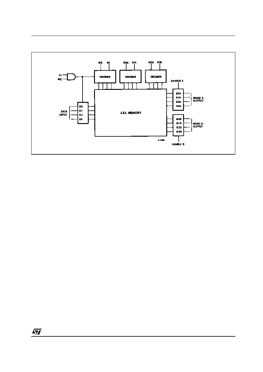
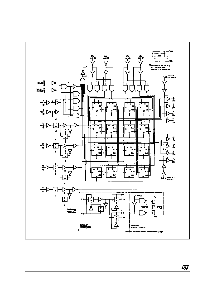
HCF40208B is a 4 x 4 multiport register containing
four 4-bit registers, a write address decoder, two
separate read address decoders, and two 3-state
output buses. When the ENABLE input is low, the
corresponding output bus is switched,
independently of the clock, to a high impedance
state. The high impedance third state provides the
outputs with the capability of being connected to
the bus lines in a bus organized system without
the need for interface or pull-up components.
When the WRITE ENABLE input is high, all data
input lines are latched on the positive transition of
the CLOCK and the data is entered into the word
selected by the write address lines. When WRITE
ENABLE is low, the CLOCK is inhibited and no
new data is entered. In either case, the contents of
any word may be accessed via the read address
lines independent of the state of the CLOCK input.
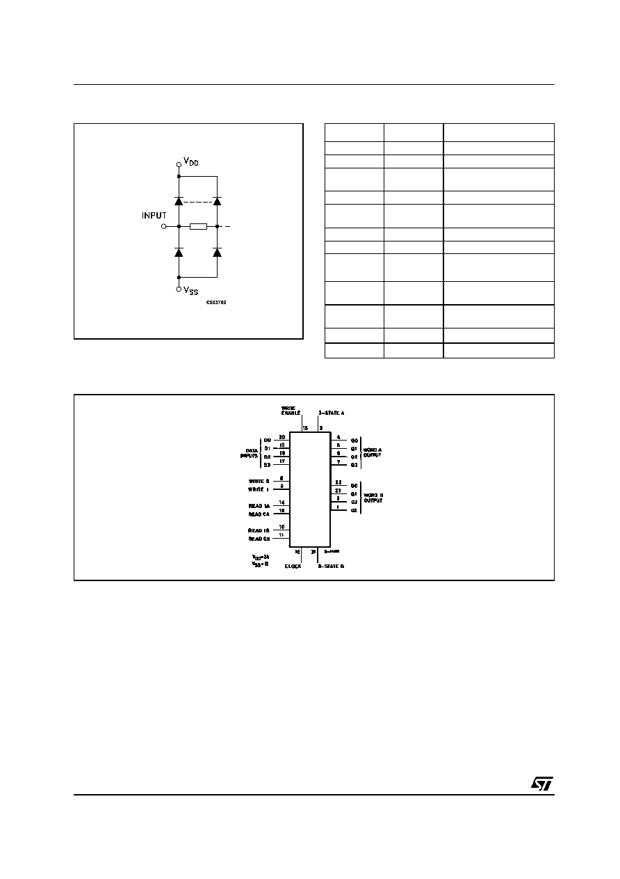
HCF40208B
4 x 4 MULTIPORT REGISTER
PIN CONNECTION
ORDER CODES
PACKAGE
TUBE
T & R
SOP
HCF40208BM1
HCF40208M013TR
SOP
HCF40208B
5/11
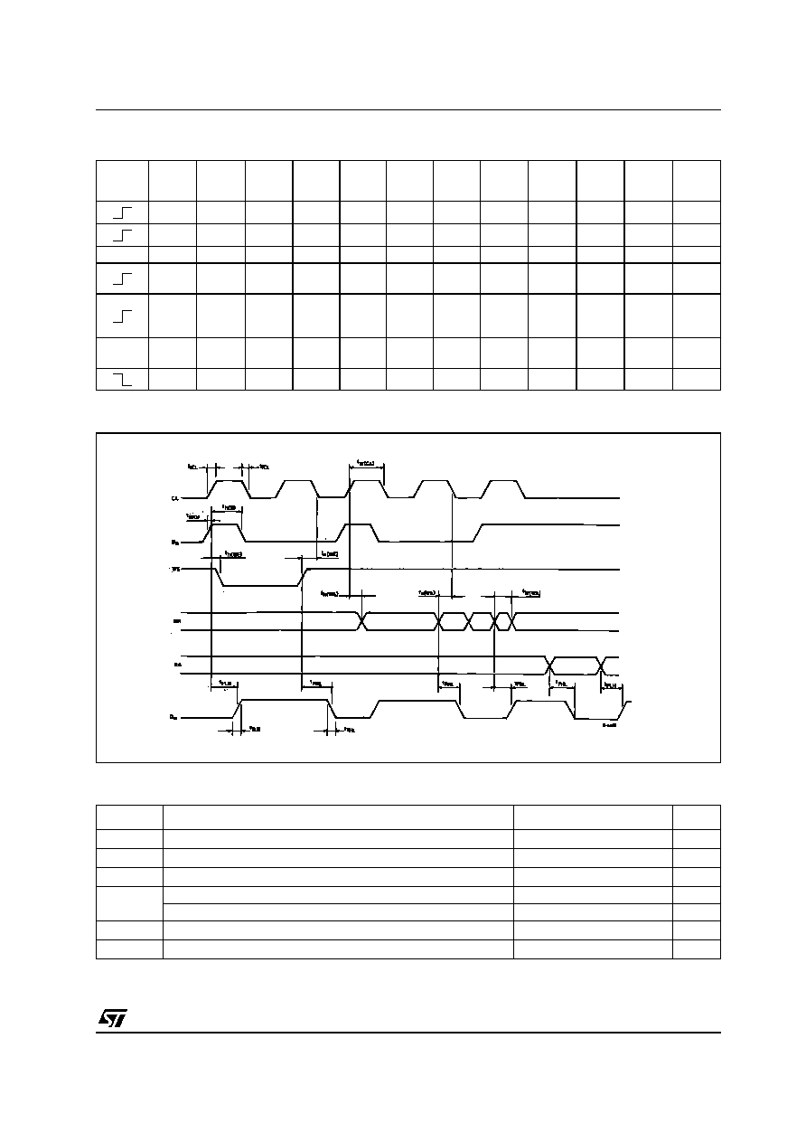
TRUTH TABLE
TIMING CHART
ABSOLUTE MAXIMUM RATINGS
Absolute Maximum Ratings are those values beyond which damage to the device may occur. Functional operation under these conditions is
not implied.
All voltage values are referred to V
SS
pin voltage.
CLOCK
Write
Enable
Write
1
Write
2
Read
1A
Read
0A
Read
1B
Read
0B
Enable
A
Enable
B
Dn
DnA
QnB
H
S1
S2
S1
S2
S1
S2
H
H
H
H
H
H
S1
S2
S1
S2
S1
S2
H
L
L
L
L
X
X
X
X
X
X
X
X
L
L
Z
Z
Z
H
L
L
L
H
H
L
H
H
Dn to
word 0
Word 1
Out
Word 2
Out
L
L
L
L
H
H
L
H
H
Word 0
not
altered
Word 1
Out
Word 2
Out
X
X
X
X
H
L
L
H
H
X
X
Word 2
Out
Word 1
Out
X
X
X
X
X
X
X
H
H
X
NC
NC
Symbol
Parameter
Value
Unit
V
DD
Supply Voltage
-0.5 to +22
V
V
I
DC Input Voltage
-0.5 to V
DD
+ 0.5
V
I
I
DC Input Current
±
10
mA
P
D
Power Dissipation per Package
200
mW
Power Dissipation per Output Transistor
100
mW
T
op
Operating Temperature
-55 to +125
∞C
T
stg
Storage Temperature
-65 to +150
∞C