1/9
September 2002
s
2 TTL-LOAD OUTPUT DRIVE CAPABILITY
s
3 STATE OUTPUTS
s
COMMON OUTPUT DISABLE CONTROL
s
INHIBIT CONTROL
s
QUIESCENT CURRENT SPECIFIED UP TO
20V
s
5V, 10V AND 15V PARAMETRIC RATINGS
s
INPUT LEAKAGE CURRENT
I
I
= 100nA (MAX) AT V
DD
= 18V T
A
= 25∞C
s
100% TESTED FOR QUIESCENT CURRENT
s
MEETS ALL REQUIREMENTS OF JEDEC
JESD13B "STANDARD SPECIFICATIONS
FOR DESCRIPTION OF B SERIES CMOS
DEVICES"
DESCRIPTION
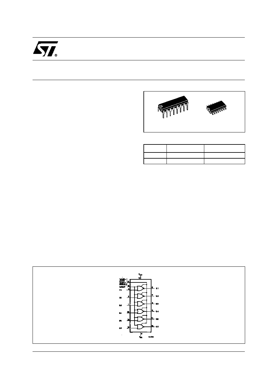
HCF4502B is a monolithic integrated circuit
fabricated in Metal Oxide Semiconductor
technology available in DIP and SOP packages.
It consists of six inverter/buffers with 3 state
outputs. A logic "1" on the OUTPUT DISABLE
input produces a High Impedance State in all six
outputs. This feature permits common busing of
the outputs, thus simplifying system design. A
logic "1" on the INHIBIT input switches all six
outputs to logic "0" if the OUTPUT DISABLE input
is a logic "0". This device is capable of driving two
standard TTL loads, which is equivalent to six
times the JEDEC "B" series I
OL
standard .
HCF4502B
STROBED HEX INVERTER/BUFFER
PIN CONNECTION
ORDER CODES
PACKAGE
TUBE
T & R
DIP
HCF4502BEY
SOP
HCF4502BM1
HCF4502M013TR
DIP
SOP
HCF4502B
2/9
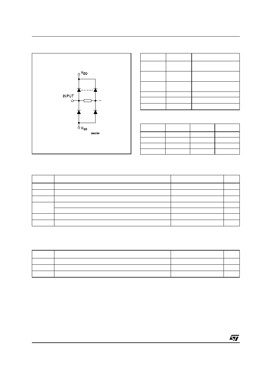
INPUT EQUIVALENT CIRCUIT
PIN DESCRIPTION
TRUTH TABLE
X : Don't Care
Z : High Impedance
ABSOLUTE MAXIMUM RATINGS
Absolute Maximum Ratings are those values beyond which damage to the device may occur. Functional operation under these conditions is
not implied.
All voltage values are referred to V
SS
pin voltage.
RECOMMENDED OPERATING CONDITIONS
PIN No
SYMBOL
NAME AND FUNCTION
3, 6, 1, 10,
13, 15
D1 to D6
Data Inputs
5, 7, 2, 9, 11,
14
Q1 to Q6
Data Outputs
4
OUTPUT
DISABLE
3-State Output Disable
Input
12
INHIBIT
Inhibit Input
8
V
SS
Negative Supply Voltage
16
V
DD
Positive Supply Voltage
DISABLE
INHIBIT
Dn
Qn
L
L
L
H
L
L
H
L
L
H
X
L
H
X
X
Z
Symbol
Parameter
Value
Unit
V
DD
Supply Voltage
-0.5 to +22
V
V
I
DC Input Voltage
-0.5 to V
DD
+ 0.5
V
I
I
DC Input Current
±
10
mA
P
D
Power Dissipation per Package
200
mW
Power Dissipation per Output Transistor
100
mW
T
op
Operating Temperature
-55 to +125
∞C
T
stg
Storage Temperature
-65 to +150
∞C
Symbol
Parameter
Value
Unit
V
DD
Supply Voltage
3 to 20
V
V
I
Input Voltage
0 to V
DD
V
T
op
Operating Temperature
-55 to 125
∞C

HCF4502B
3/9
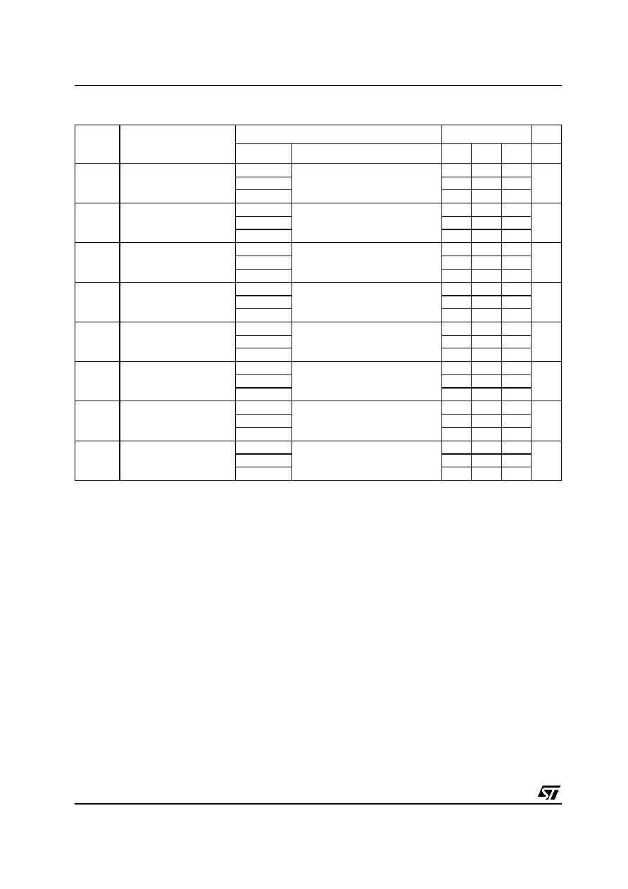
DC SPECIFICATIONS
The Noise Margin for both "1" and "0" level is: 1V min. with V
DD
=5V, 2V min. with V
DD
=10V, 2.5V min. with V
DD
=15V
Symbol
Parameter
Test Condition
Value
Unit
V
I
(V)
V
O
(V)
|I
O
|
(
µ
A)
V
DD
(V)
T
A
= 25∞C
-40 to 85∞C
-55 to 125∞C
Min.
Typ.
Max.
Min.
Max.
Min.
Max.
I
L
Quiescent Current
0/5
5
0.02
1
30
30
µ
A
0/10
10
0.02
2
60
60
0/15
15
0.02
4
120
120
0/20
20
0.04
20
600
600
V
OH
High Level Output
Voltage
0/5
<1
5
4.95
4.95
4.95
V
0/10
<1
10
9.95
9.95
9.95
0/15
<1
15
14.95
14.95
14.95
V
OL
Low Level Output
Voltage
5/0
<1
5
0.05
0.05
0.05
V
10/0
<1
10
0.05
0.05
0.05
15/0
<1
15
0.05
0.05
0.05
V
IH
High Level Input
Voltage
0.5/4.5
<1
5
3.5
3.5
3.5
V
1/9
<1
10
7
7
7
1.5/13.5
<1
15
11
11
11
V
IL
Low Level Input
Voltage
4.5/0.5
<1
5
1.5
1.5
1.5
V
9/1
<1
10
3
3
3
13.5/1.5
<1
15
4
4
4
I
OH
Output Drive
Current
0/5
2.5
<1
5
-1.36
-3.2
-1.15
-1.15
mA
0/5
4.6
<1
5
-0.44
-1
-0.36
-0.36
0/10
9.5
<1
10
-1.1
-2.6
-0.9
-0.9
0/15
13.5
<1
15
-3.0
-6.8
-2.4
-2.4
I
OL
Output Sink
Current
0/5
0.4
<1
5
2.6
6
2.1
2.1
mA
0/10
0.5
<1
10
6.63
15.6
5.4
5.4
0/15
1.5
<1
15
17.3
40.8
14.2
14.2
I
I
Input Leakage
Current
0/18
Any Input
18
±
10
-5
±
0.1
±
1
±
1
µ
A
I
OZ
3-State Output
0/18
Any Input
18
±
10
-4
±
0.4
±
12
±
12
µ
A
C
I
Input Capacitance
Any Input
5
7.5
pF
HCF4502B
4/9
DYNAMIC ELECTRICAL CHARACTERISTICS (T
amb
= 25∞C, C
L
= 50pF, R
L
= 200K
, t
r
= t
f
= 20 ns)
(*) Typical temperature coefficent for all V
DD
value is 0.3 %/∞C.
Symbol
Parameter
Test Condition
Value (*)
Unit
V
DD
(V)
Min.
Typ.
Max.
t
PHL
Propagation Delay Time
(Data or Inhibit)
5
135
270
ns
10
60
120
15
40
80
t
PLH
Propagation Delay Time
(Data or Inhibit)
5
190
380
ns
10
90
180
15
65
30
t
PHZ
Disable Delay Time
(Output High to High
Impedance)
5
60
120
ns
10
40
80
15
30
60
t
PZH
Disable Delay Time
(High Impedance to Output
High)
5
110
220
ns
10
50
100
15
40
80
t
PLZ
Disable Delay Time
(Output Low to High
Impedance)
5
125
250
ns
10
65
130
15
55
110
t
PZL
Disable Delay Time
(High Impedance to Output
Low)
5
125
250
ns
10
55
110
15
40
80
t
TLH
Transition Time
5
100
200
ns
10
50
100
15
40
80
t
THL
Transition Time
5
60
120
ns
10
30
60
15
20
40
HCF4502B
5/9
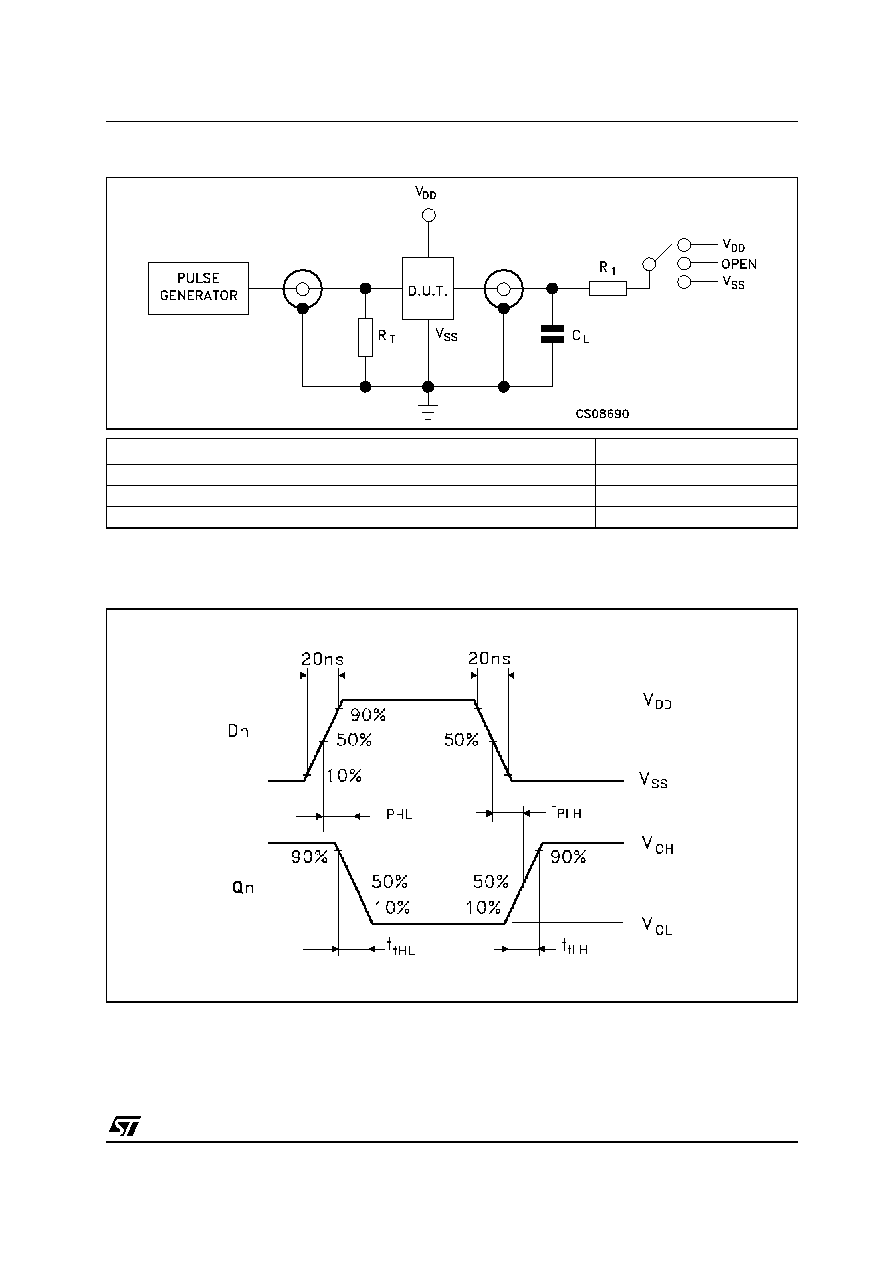
TEST CIRCUIT
C
L
= 50pF or equivalent (includes jig and probe capacitance)
R
L
= 200K
R
T
= Z
OUT
of pulse generator (typically 50
)
WAVEFORM 1: PROPAGATION DELAY TIMES (f=1MHz; 50% duty cycle)
TEST
SWITCH
t
PLH
, t
PHL
Open
t
PZL
, t
PLZ
V
DD
t
PZH
, t
PHZ
V
SS