July 1992
IMAGE AND SIGNAL PROCESSING SUB≠SYSTEM
IMSA110
.
1-D/2-D SOFTWARE CONFIGURABLE CON-
VOLVER/FILTER
.
ON-CHIP PROGRAMMABLE LINE DELAYS (0
-- 1120 STAGES)
.
8-BIT DATA AND 8.5-BIT COEFFICIENT
SLICE
.
21 MULTIPLY-AND-ACCUMULATE STAGES
.
1-D (21) OR 2-D (3 x 7) CONVOLUTION WIN-
DOW
.
ON-CHIP POST PROCESSOR FOR DATA
TRANSFORMATION
.
FULLY CASCADABLE IN WINDOW SIZE AND
ACCURACY
.
20 MHZ DATA THROUGHPUT (420 MOPS)
.
SIGNED/UNSIGNED DATA AND COEFFI-
CIENTS
.
MICROPROCESSOR INTERFACE
.
HIGH SPEED CMOS IMPLEMENTATION
.
TTL COMPATIBLE
.
SINGLE +5V
±
10% SUPPLY
.
POWER DISSIPATION < 2.0 WATTS
.
100 PIN CERAMIC PGA
APPLICATIONS
.
1-D and 2-D digital convolution and correlation
.
Real time image processing and enhancement
.
Edge and feature detection
.
Data transformation and histogram equalisa-
tion
.
Computer vision and robotics
.
Template matching
.
Pulse compression
.
1-D or 2-D interpolation
ORDERING INFORMATION
Part Number
Package
Clock
Speed
Military/
commercial
IMSA110-G20S
PGA100
20MHz
commercial
A1
1
0
-0
1
.
T
B
L
PGA100
(Ceramic Grid Array Package)
1/26
Notes : 1. All V
CC
pins must be connected to the 5 Volt power supply.
2. All GND pins must be connected to ground.
RESET
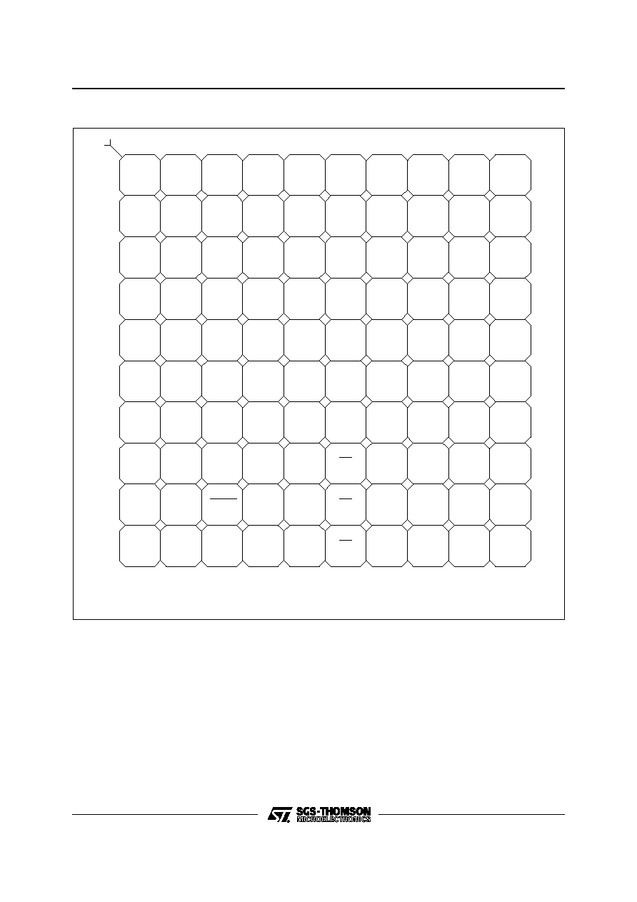
Vcc
A
B
C
D
E
F
G
H
J
K
1
2
3
4
5
6
7
8
9
10
Index
PSRIN
[6]
PSRIN
[4]
PSRIN
[2]
PSRIN
[1]
CIN
[3]
CLK
PSRIN
[7]
CIN
[4]
CIN
[0]
CIN
[2]
Vcc
GND
CIN
[5]
CIN
[8]
CIN
[6]
CIN
[7]
CIN
[13]
CIN
[15]
CIN
[17]
CIN
[14]
CIN
[19]
CIN
[21]
CIN
[16]
CIN
[20]
W
CIN
[18]
ADR
[0]
ADR
[1]
PSRIN
[3]
PSRIN
[5]
GND
PSROUT
[0]
PSROUT
[1]
PSROUT
[2]
GND
PSROUT
[3]
PSROUT
[5]
PSROUT
[6]
PSROUT
[7]
COUT
[0]
COUT
[2]
COUT
[4]
COUT
[1]
GND
COUT
[6]
COUT
[7]
COUT
[9]
Vcc
COUT
[10]
COUT
[12]
COUT
[13]
COUT
[14]
Vcc
GND
COUT
[15]
COUT
[19]
COUT
[18]
COUT
[17]
Vcc
Vcc
D[5]
D[7]
COUT
[21]
D[3]
D[4]
D[1]
GND
D[2]
D[0]
ADR
[7]
ADR
[6]
ADR
[8]
ADR
[2]
ADR
[3]
E1
E2
CIN
[1]
CIN
[12]
ADR
[5]
Vcc
GND
GND
GND
GND
GND
PSRIN
[0]
PSROUT
[4]
COUT
[8]
COUT
[3]
COUT
[11]
COUT
[16]
D[6]
COUT
[5]
CIN
[9]
CIN
[10]
CIN
[11]
ADR
[4]
COUT
[20]
A1
1
0
-0
1
.
EP
S
PIN CONNECTIONS
1. INTRODUCTION
The IMSA110 is a single-chip reconfigurable and
cascadable subsystem suitable for many high
speed image and signal processing applications.
Apart from its powerful multiply-accumulate capa-
bility (420 MOPs), the strength of the IMSA110 lies
in its extensive programmable support for data
conditioning and transformation.
2. DESCRIPTION
The IMSA110 consists of a configurable array of
multiply-accumulators, three programmable length
1120 stage shift registers, a versatile post-process-
ing unit and a microprocessor interface for configu-
ration and control purposes. The comprehensive
on-chip facilities make a single device capable of
dealing with many image processing operations.
IMSA110
2/26
Decode
logic
21 x 8-bit
Update coefficient registers
21 x 8-bit
Current coefficient registers
256 x 8-bit data
transformation
look up RAM
Backend
look up table
USR
LSR
PCR0
PCR1
PCR2
BCR
MMB
OUB
TCR
SCR
ACR
Configuration and
control registers
Control
logic
1120 stage Programmable
shift register (PSRB)
1120 stage Programmable
shift register (PSRA)
7-stage
multiply-accumulate
array B
7-stage
multiply-accumulate
array A
1120 stage Programmable
shift register (PSRC)
7-stage
multiply-accumulate
array C
D
22
22
8
22
8
8
9
CLOCK
RESET
CASCADE
INPUT
CASCADE
OUTPUT
PSROUT
ADDRESS
PSRIN
MEM
DATA
Synchronous Functions
ENABLE 1
ENABLE 2
WRITE
Asynchronous Functions
Backend
post-processing unit
(normalization, saturation,
and data transformation)
A
1
1
0
-0
2
.
EPS
Figure 1 : IMSA110 Users Model
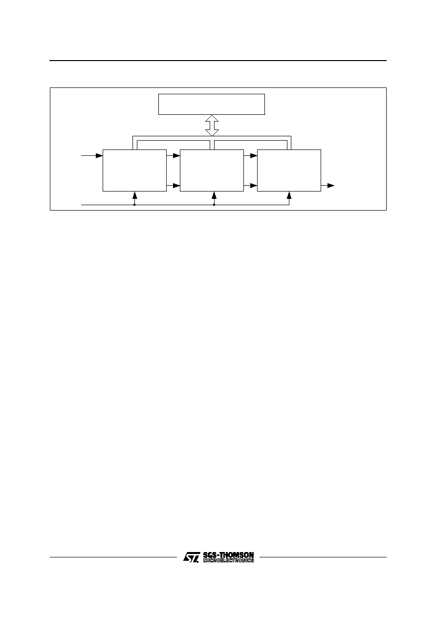
The IMSA110 has five interfaces through which
data can be transferred, Figure 1. The microproc-
essor interface allows access to the coefficient
registers, the configuration and status registers,
and the data transformation tables. The remaining
four interfaces allow high speed data input and
output to the IMSA110 and the cascading of several
devices. A typical IMSA110 system is shown in
Figure 3. If N devices are used in the cascade, they
can be configured, entirely under software control,
as a 21N stage 1-D transversal filter or as a 7X by
3Y 2-D window, where X and Y are any integers
satisfying N
XY. For example 4 cascaded devices
can be software configured as: an 84-stage 1-D
filter, a 7 by 12 2-D window, a 28 by 3 2-D window,
or a 14 by 6 2-D window.
The final output of the chip is 22 bits wide in twos
complement format.
Figure 2 shows the distribution of the delays inside
the part.
The latency between PSRin and COUT is depend-
ent upon the length of PSRc. For example, with
PSRc set to 0, and all coefficients set to zero except
CR0c[6] (so the data passes through all MAC
stages), the COUT bus will correspond to the
PSRin bus delayed by 47 clock cycles.
The latency between PSRin and PSRout is 5 cycles
PLUS the lengths of PSRc, PSRb and PSRa. If the
shift registers are bypassed by setting SCR[1] to 1
then PSRout will be PSRin delayed by 2 clock
cycles.
The Latency between the cascade input (CIN) and
cascade output (COUT) is 6 cycles. This is shown
lumped at the cascade input and cascade output
pads in Figure 2. Figure 4 gives details of the data
pipelining through the backend datapath.
IMSA110
3/26
X
D
X
D
X
X
D
D
D
CR1c coefficient registers 7 x 8 bits
CR0c coefficient registers 7 x 8 bits
3
1
1
1
1
D
22
X
D
X
D
X
X
D
D
D
3
1
1
1
1
D
22
X
D
X
D
X
X
D
D
D
3
1
1
1
1
D
22
CR1b coefficient registers 7 x 8 bits
CR0b coefficient registers 7 x 8 bits
CR1a coefficient registers 7 x 8 bits
CR0a coefficient registers 7 x 8 bits
D
D
D
D
D
D
1
2
1
1
2
1
1
2
1
Programmable PSRC
shift register
0 to 1120 stages
D
1
8
8
MUX
8
8
Programmable PSRA
shift register
0 to 1120 stages
Programmable PSRB
shift register
0 to 1120 stages
D
1
13
D
D
22
5
1
2
1
2
Backend processing unit
including cascade data path,
normalization, saturation units and
data transformation look up tables
(see Figure 4 for detail)
cascade input
cascade output
COUT
CIN
PSROUT
PSRIN
A
1
1
0
-0
3
.
EPS
Figure 2 : Synchronous Functions of the IMSA110
IMSA110
4/26
General purpose
microprocessor
IMSA110
PSRIN
Cascade
IN
PSROUT
Cascade
OUT
Input
Clock
Output
IMSA110
PSRIN
Cascade
IN
PSROUT
Cascade
OUT
IMSA110
PSRIN
Cascade
IN
PSROUT
Cascade
OUT
A1
1
0
-0
4
.
EP
S
Figure 3 : A Typical IMSA110 Based System
3. PROGRAMMABLE SHIFT REGISTERS
The three shift registers are 8 bits wide and are
each programmable from 0 up to 1120 clock cycles
in length. The lengths are programmed into control
registers via the microprocessor interface.
Data is clocked into the device via the PSRin bus
(Programmable Shift Register in) at a maximum
rate of 20MHz. On-chip, the input data is then fed
through a pipeline of the three shift registers. The
output of the first shift register passes to the first
7-stage mac array and also to the input of the
second shift register. Having passed through all
three shift registers the data is output on the
PSRout bus and can be used for cascading. Alter-
natively, as shown in Figure 2 the shift registers can
be bypassed and the input data transferred to the
PSRout bus after two delay stages. This mode can
be controlled via the on-chip control registers and
significantly simplifies software configuration of a
cascade arrangement.
4. MAC ARRAY
As shown in Figure 2, the processing core of the
device consists of a configurable array of multiply-
accumulators (macs). The mac array consists of
three 7-stage transversal filters which can be con-
figured either as a 21-stage linear pipeline or as a
3
◊
7 two-dimensional window. The input data is
8 bits wide and is fed to the mac array via three
programmable shift registers.
The output of each shift register is supplied as input
to one of the three 7-stage transversal filters. For
each of the three transversal filters the associated
input data is fed simultaneously to all 7 mac stages.
At each stage the input sample is multiplied by a
coefficient stored in memory, and added to the
output of the previous stage delayed by one clock
cycle. The output of each 7-stage mac is fed, via a
delay stage, to the first stage in the next transversal
filter.
The coefficient word width in the mac array is 8 bits
wide. Two banks of coefficients are provided. At any
instant one set of coefficients is in use within the
mac array. The set in use is defined by the state of
the `Current Bank' bit, ACR[0]. The other set can be
altered via the microprocessor interface. Once a
new set of coefficients has been loaded, the activi-
ties of the two coefficient banks can be inter-
changed without interrupting the flow of data. Alter-
natively, by setting the `continous bank swap' bit
SCR[0], the two coefficient banks are swapped
automatically after each data input. In this case the
`Current Bank' bit only determines which bank is
used first. Both data input and coefficients can be
programmed independently to support twos com-
plement or positive unsigned formats allowing mul-
tiple devices to be used as a `slice' in higher accu-
racy systems.
Within the mac array no truncation or rounding is
performed on the partial products. The mac array
output is fed to the backend post-processing unit
which is responsible for data transformation / nor-
malisation and cascading function.
5. BACKEND POST-PROCESSOR -- hardware
description
The Backend Post-Processor consists of four ma-
jor blocks : The input block (shifter, cascade adder
and rectifier unit),a statistics monitor,the data con-
ditioning unit which itself consists of the data trans-
formation unit and the data normaliser, and the
output block (output adder and multiplexers).
A detailed diagram of the Backend Post-Processor
is given in Figure 4.
All operations performed in the backend are on
twos complement signed numbers unless other-
wise stated.
IMSA110
5/26