Link adaptor
IMS C011
)
July 1995
1/30
FEATURES
APPLICATIONS
H
Standard INMOS link protocol
H
10 or 20 Mbits/sec operating speed
H
Communicates with transputers
H
Converts between serial link and parallel bus
H
Converts between serial link and parallel device
H
Two modes of parallel operation:
Mode 1: Peripheral interface
Eight bit parallel input interface
Eight bit parallel output interface
Full handshake on input and output
Mode 2: Bus interface
Tristate bidirectional bus interface
Memory mapped registers
Interrupt capability
H
Single +5V
5% power supply
H
TTL and CMOS compatibility
H
120mW power dissipation
H
28 pin 0.6" plastic package
H
28 pin SOJ package
H
28 pin LCCC package
H
Extended temperature version available
H
Programmable I/O for transputer
H
Connecting microprocessors to transputers
H
High speed links between microprocessors
H
Inter-family microprocessor interfacing
H
Interconnecting different speed links
Input
Interface
System
Services
8
Output
Interface
8
Link
Mode 1
8
Mode 2
Interrupt
Control
System
Services
Data and
Status
Registers
Link
Register
Select
42 1412 08

Contents
/ 30
2
1 Introduction
3
. . . . . . . . . . . . . . . . . . . . . . . . . . . . . . . . . . . . . . . . . . . . . . . . . . . . . .
2 Pin designations
4
. . . . . . . . . . . . . . . . . . . . . . . . . . . . . . . . . . . . . . . . . . . . . . . . . .
3 System services
5
. . . . . . . . . . . . . . . . . . . . . . . . . . . . . . . . . . . . . . . . . . . . . . . . . .
3.1
Power
5
. . . . . . . . . . . . . . . . . . . . . . . . . . . . . . . . . . . . . . . . . . . . . . . . . . . . . . . . . . . . . . . . . . . . .
3.2
CapMinus
5
. . . . . . . . . . . . . . . . . . . . . . . . . . . . . . . . . . . . . . . . . . . . . . . . . . . . . . . . . . . . . . . . .
3.3
ClockIn
5
. . . . . . . . . . . . . . . . . . . . . . . . . . . . . . . . . . . . . . . . . . . . . . . . . . . . . . . . . . . . . . . . . . . .
3.4
SeparateIQ
6
. . . . . . . . . . . . . . . . . . . . . . . . . . . . . . . . . . . . . . . . . . . . . . . . . . . . . . . . . . . . . . . .
3.5
Reset
7
. . . . . . . . . . . . . . . . . . . . . . . . . . . . . . . . . . . . . . . . . . . . . . . . . . . . . . . . . . . . . . . . . . . . .
4 Links
9
. . . . . . . . . . . . . . . . . . . . . . . . . . . . . . . . . . . . . . . . . . . . . . . . . . . . . . . . . . . . .
5 Mode 1 parallel interface
12
. . . . . . . . . . . . . . . . . . . . . . . . . . . . . . . . . . . . . . . . . . .
5.1
Input port
12
. . . . . . . . . . . . . . . . . . . . . . . . . . . . . . . . . . . . . . . . . . . . . . . . . . . . . . . . . . . . . . . . . .
5.2
Output port
13
. . . . . . . . . . . . . . . . . . . . . . . . . . . . . . . . . . . . . . . . . . . . . . . . . . . . . . . . . . . . . . . .
6 Mode 2 parallel interface
14
. . . . . . . . . . . . . . . . . . . . . . . . . . . . . . . . . . . . . . . . . . .
6.1
D0≠7
14
. . . . . . . . . . . . . . . . . . . . . . . . . . . . . . . . . . . . . . . . . . . . . . . . . . . . . . . . . . . . . . . . . . . . . .
6.2
notCS
14
. . . . . . . . . . . . . . . . . . . . . . . . . . . . . . . . . . . . . . . . . . . . . . . . . . . . . . . . . . . . . . . . . . . . .
6.3
RnotW
14
. . . . . . . . . . . . . . . . . . . . . . . . . . . . . . . . . . . . . . . . . . . . . . . . . . . . . . . . . . . . . . . . . . . .
6.4
RS0≠1
14
. . . . . . . . . . . . . . . . . . . . . . . . . . . . . . . . . . . . . . . . . . . . . . . . . . . . . . . . . . . . . . . . . . . .
6.5
InputInt
17
. . . . . . . . . . . . . . . . . . . . . . . . . . . . . . . . . . . . . . . . . . . . . . . . . . . . . . . . . . . . . . . . . . . .
6.6
OutputInt
18
. . . . . . . . . . . . . . . . . . . . . . . . . . . . . . . . . . . . . . . . . . . . . . . . . . . . . . . . . . . . . . . . . .
6.7
Data read
18
. . . . . . . . . . . . . . . . . . . . . . . . . . . . . . . . . . . . . . . . . . . . . . . . . . . . . . . . . . . . . . . . . .
6.8
Data write
18
. . . . . . . . . . . . . . . . . . . . . . . . . . . . . . . . . . . . . . . . . . . . . . . . . . . . . . . . . . . . . . . . .
7 Electrical specifications
19
. . . . . . . . . . . . . . . . . . . . . . . . . . . . . . . . . . . . . . . . . . .
7.1
DC electrical characteristics
19
. . . . . . . . . . . . . . . . . . . . . . . . . . . . . . . . . . . . . . . . . . . . . . . . . .
7.2
Equivalent circuits
20
. . . . . . . . . . . . . . . . . . . . . . . . . . . . . . . . . . . . . . . . . . . . . . . . . . . . . . . . . .
7.3
AC timing characteristics
21
. . . . . . . . . . . . . . . . . . . . . . . . . . . . . . . . . . . . . . . . . . . . . . . . . . . .
7.4
Power rating
23
. . . . . . . . . . . . . . . . . . . . . . . . . . . . . . . . . . . . . . . . . . . . . . . . . . . . . . . . . . . . . . .
8 Package details
24
. . . . . . . . . . . . . . . . . . . . . . . . . . . . . . . . . . . . . . . . . . . . . . . . . . .
8.1
Package pinouts
24
. . . . . . . . . . . . . . . . . . . . . . . . . . . . . . . . . . . . . . . . . . . . . . . . . . . . . . . . . . . .
8.2
28-pin plastic DIL package dimensions
25
. . . . . . . . . . . . . . . . . . . . . . . . . . . . . . . . . . . . . . . .
8.3
28-pin SOJ package dimensions
26
. . . . . . . . . . . . . . . . . . . . . . . . . . . . . . . . . . . . . . . . . . . . . .
8.4
28-pin LCCC package dimensions
27
. . . . . . . . . . . . . . . . . . . . . . . . . . . . . . . . . . . . . . . . . . . .
8.5
Thermal specification
28
. . . . . . . . . . . . . . . . . . . . . . . . . . . . . . . . . . . . . . . . . . . . . . . . . . . . . . .
9 Ordering
29
. . . . . . . . . . . . . . . . . . . . . . . . . . . . . . . . . . . . . . . . . . . . . . . . . . . . . . . . . .

/ 30
3
1
Introduction
The INMOS communication link is a high speed system interconnect which provides full duplex communi-
cation between members of the transputer family, according to the INMOS serial link protocol. The
IMS C011, a member of this family, provides for full duplex transputer link communication with standard
microprocessor and sub-system architectures, by converting bi-directional serial link data into parallel
data streams.
All transputer products which use communication links, regardless of device type, support a standard com-
munications frequency of 10 Mbits/sec; most products also support 20 Mbits/sec. Products of different
type or performance can, therefore, be interconnected directly and future systems will be able to communi-
cate directly with those of today. The IMS C011 link will run at either the standard speed of 10 Mbits/sec
or at the higher speed of 20 Mbits/sec. Data reception is asynchronous, allowing communication to be in-
dependent of clock phase.
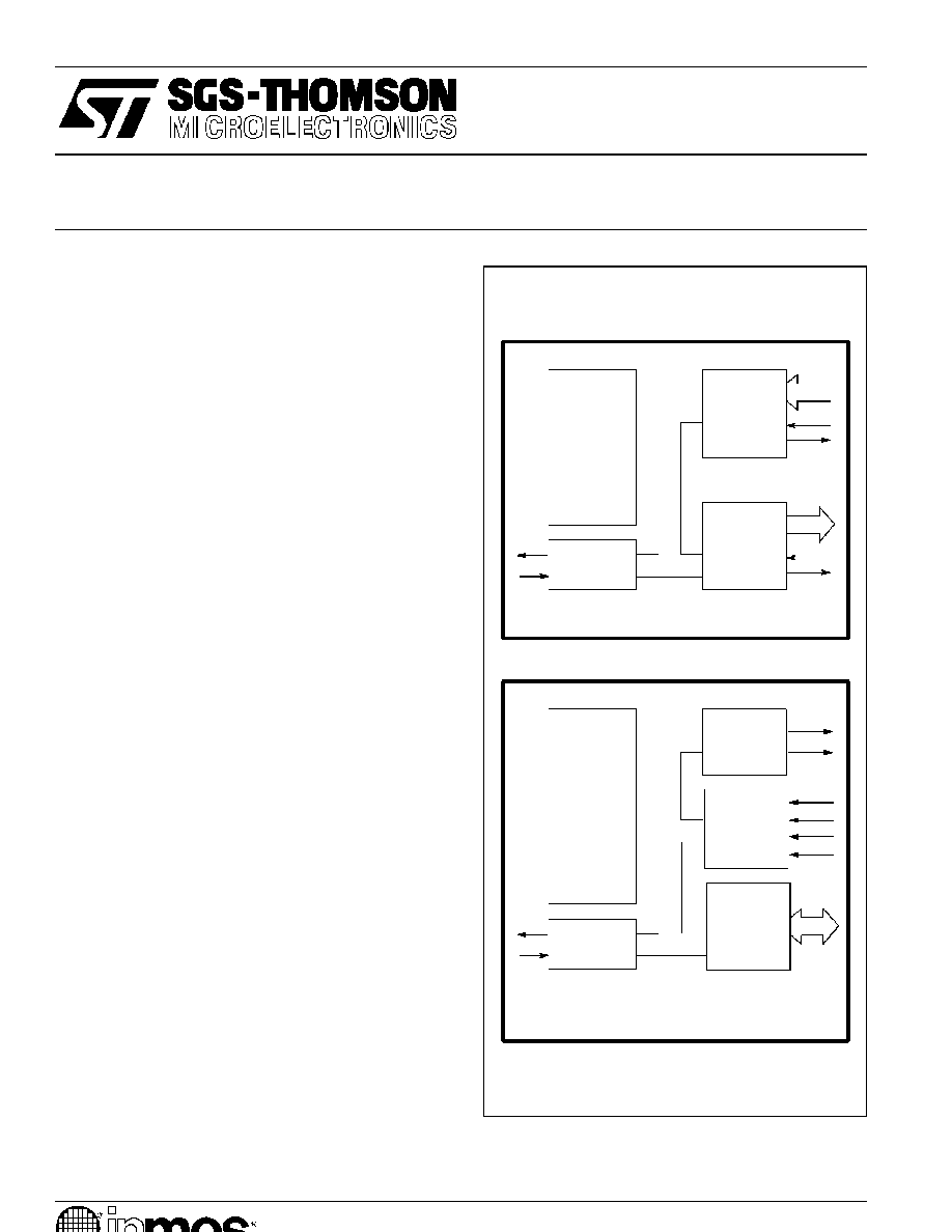
The link adaptor can be operated in one of two modes. In Mode 1 the IMS C011 converts between a link
and two independent fully handshaken byte-wide interfaces, one input and one output. It can be used by
a peripheral device to communicate with a transputer, a peripheral processor or another link adaptor, or
it can provide programmable input and output pins for a transputer. Two IMS C011 devices in this mode
can be connected back to back via the parallel ports and used as a frequency changer between different
speed links.
In Mode 2 the IMS C011 provides an interface between an INMOS serial link and a microprocessor system
bus. Status and data registers for both input and output ports can be accessed across the byte-wide
bi-directional interface. Two interrupt outputs are provided, one to indicate input data available and one
for output buffer empty.
Input
Interface
Output
Interface
System
Services
Link
8
8
Q0≠7
Qack
QValid
I0≠7
IAck
IValid
VDD
GND
CapMinus
ClockIn
Reset
SeparateIQ
LinkOut
LinkIn
Figure 1.1
IMS C011 Mode 1 block diagram
Interrupt
Control
Data and
Status
Registers
System
Services
Link
8
D0≠7
InputInt
OutputInt
VDD
GND
CapMinus
ClockIn
Reset
SeparateIQ
LinkOut
LinkIn
Register
Select
LinkSpeed
RS0
RS1
RnotW
notCS
Figure 1.2
IMS C011 Mode 2 block diagram

IMS C011
/ 30
4
2
Pin designations
Signal names are prefixed by not if they are active low, otherwise they are active high.
Pinout details for various packages are given on page 24.
Pin
In/Out
Function
VDD, GND
Power supply and return
CapMinus
External capacitor for internal clock power supply
ClockIn
in
Input clock
Reset
in
System reset
SeparateIQ
in
Select mode and Mode 1 link speed
LinkIn
in
Serial data input channel
LinkOut
out
Serial data output channel
Table 2.1
Services and link
Pin
In/Out
Function
I0-7
in
Parallel input bus
IValid
in
Data on I0-7 is valid
IAck
out
Acknowledge I0-7 data received by other link
Q0-7
out
Parallel output bus
QValid
out
Data on Q0-7 is valid
QAck
in
Acknowledge from device: data Q0-7 was read
Table 2.2
Mode 1 parallel interface
Pin
In/Out
Function
D0-7
in/out
Bi-directional data bus
notCS
in
Chip select
RS0-1
in
Register select
RnotW
in
Read/write control signal
InputInt
out
Interrupt on link receive buffer full
OutputInt
out
Interrupt on link transmit buffer empty
LinkSpeed
in
Select link speed as 10 or 20 Mbits/sec
HoldToGND
Must be connected to GND
DoNotWire
Must not be wired
Table 2.3
Mode 2 parallel interface
3 System services
/ 30
5
3
System services
System services include all the necessary logic to start up and maintain the IMS C011.
3.1
Power
Power is supplied to the device via the VDD and GND pins. The supply must be decoupled close to the
chip by at least one 100 nF low inductance (e.g. ceramic) capacitor between VDD and GND. Four layer
boards are recommended; if two layer boards are used, extra care should be taken in decoupling.
AC noise between VDD and GND must be kept below 200 mV peak to peak at all frequencies above
100 KHz. AC noise between VDD and the ground reference of load capacitances must be kept below
200 mV peak to peak at all frequencies above 30 MHz. Input voltages must not exceed specification with
respect to VDD and GND, even during power-up and power-down ramping, otherwise
latchup can occur.
CMOS devices can be permanently damaged by excessive periods of latchup.
3.2
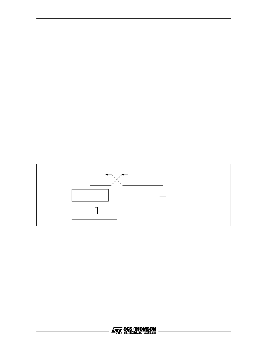
CapMinus
The internally derived power supply for internal clocks requires an external low leakage, low inductance
1
m
F capacitor to be connected between VDD and CapMinus. A ceramic capacitor is preferred, with an
impedance less than 3 Ohms between 100 KHz and 10 MHz. If a polarised capacitor is used the negative
terminal should be connected to CapMinus. Total PCB track length should be less than 50 mm. The posi-
tive connection of the capacitor must be connected directly to VDD. Connections must not otherwise touch
power supplies or other noise sources.
Phase≠locked
loops
VDD
GND
CapMinus
P.C.B track
P.C.B track
Decoupling
capacitor 1
m
F
pin
VDD
Figure 3.1
Recommended PLL decoupling
3.3
ClockIn
Transputer family components use a standard clock frequency, supplied by the user on the ClockIn input.
The nominal frequency of this clock for all transputer family components is 5 MHz, regardless of device
type, transputer word length or processor cycle time. High frequency internal clocks are derived from
ClockIn, simplifying system design and avoiding problems of distributing high speed clocks externally.
A number of transputer family devices may be connected to a common clock, or may have individual clocks
providing each one meets the specified stability criteria. In a multi-clock system the relative phasing of
ClockIn clocks is not important, due to the asynchronous nature of the links. Mark/space ratio is unimpor-
tant provided the specified limits of ClockIn pulse widths are met.
Oscillator stability is important. ClockIn must be derived from a crystal oscillator; RC oscillators are not
sufficiently stable. ClockIn must not be distributed through a long chain of buffers. Clock edges must be
monotonic and remain within the specified voltage and time limits.