 | –≠–ª–µ–∫—Ç—Ä–æ–Ω–Ω—ã–π –∫–æ–º–ø–æ–Ω–µ–Ω—Ç: L165V | –°–∫–∞—á–∞—Ç—å:  PDF PDF  ZIP ZIP |

1/9
L165
July 2003
s
OUTPUT CURRENT UP TO 3A
s
LARGE COMMON-MODE AND
DIFFERENTIAL MODE RANGES
s
SOA PROTECTION
s
THERMAL PROTECTION
s
± 18V SUPPLY
DESCRIPTION
The L165 is a monolithic integrated circuit in Pen-
tawattÆ package, intended for use as power oper-
ational amplifier in a wide range of applications,
including servo amplifiers and power supplies. The
high gain and high output power capability provide
superiore performance wherever an operational
amplifier/power booster combination is required.
Pentawatt V
ORDERING NUMBER: L165V
3A POWER OPERATIONAL AMPLIFIER
APPLICATION CIRCUITS
Figure 1. Gain > 10.
Figure 2. Unity gain configuration.
L165
2/9
ABSOLUTE MAXIMUM RATINGS
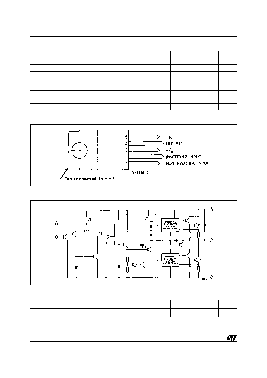
PIN CONNECTION (Top view)
SCHEMATIC DIAGRAM
THERMAL DATA
Symbol
Parameter
Value
Unit
V
S
Supply voltage
± 18
V
V
5
V
4
Upper power transistor V
CE
36
V
V
4
V
3
Lower power transistor V
CE
36
V
V
i
Input voltage
V
S
V
j
Differential input voltage
±
15
V
I
o
Peak output current (internally limited)
3.5
A
P
tot
Power dissipation at T
case
= 90∞C
20
W
T
stg
, T
j
Storage and junction temperature
-40 to 150
∞
C
Symbol
Parameter
Value
Unit
R
th-j-case
Thermal resistance junction-case
max
3
∞C/W

3/9
L165
ELECTRICAL CHARACTERISTCS (V
S
= ± 15 V, T
j
= 25 ∞C unless otherwise specified)
Symbol
Parameter
Test Condition
Min.
Typ.
Max.
Unit
V
S
Supply Voltage
±
6
±
18
V
I
d
Quiescent Drain Current
V
S
= ±18 V
40
60
mA
I
b
Input Bias Current
0.2
1
µ
A
V
os
Input Offset Voltage
±
2
±
10
mV
I
os
Input Offset Current
±
20
±
200
nA
SR
Slew-rate
G
v
= 10
8
V/
µ
s
G
v
= 1 (∞)
6
V
o
Output Voltage Swing
f = 1kHz
I
p
=
0.3A
I
p
= 3A
27
24
V
pp
f = 10kHz
I
p
=
0.3A
I
p
= 3A
27
24
V
pp
R
Input Resistance (pin 1)
f = 1 KHz
100
500
K
G
v
Voltage Gain (open loop)
80
dB
e
N
Input Noise Voltage
B = 10 to 10 000 Hz
2
µ
V
i
N
Input Noise Current
f = 1 KHz
100
pA
CMR
Common-mode Rejection
R
g
10 K
; G
V
= 30 dB
70
dB
SVR
Supply Voltage Rejection
R
g
= 22 K
; V
ripple
= 0.5 Vrms
f
ripple
= 100 Hz
G
v
= 10
G
v
= 100
60
40
dB
dB
Efficiency
f = 1 kHz; R
L
= 4
I
p
= 1.6 A; P
o
= 5W
I
p
= 1.6 A; P
o
= 18W
70
60
%
%
T
sd
Thermal Shut-down Case
Temperature
P
tot
= 12 W
110
∞
C
P
tot
= 6 W
130
∞
C

L165
4/9
Figure 3. Open loop frequency response.
Figure 4. Closed loop frequency response
(circuit of figure 2).
Figure 5. Large signal frequency response.
Figure 6. Maximum output current vs. voltage
[VCE] across each output transistor.
Figure 7. Safe operating area and collector
characteristics of the protected
power transistor.
Figure 8. Maximum allowable power
dissipation vs. ambient temperature.
5/9
L165
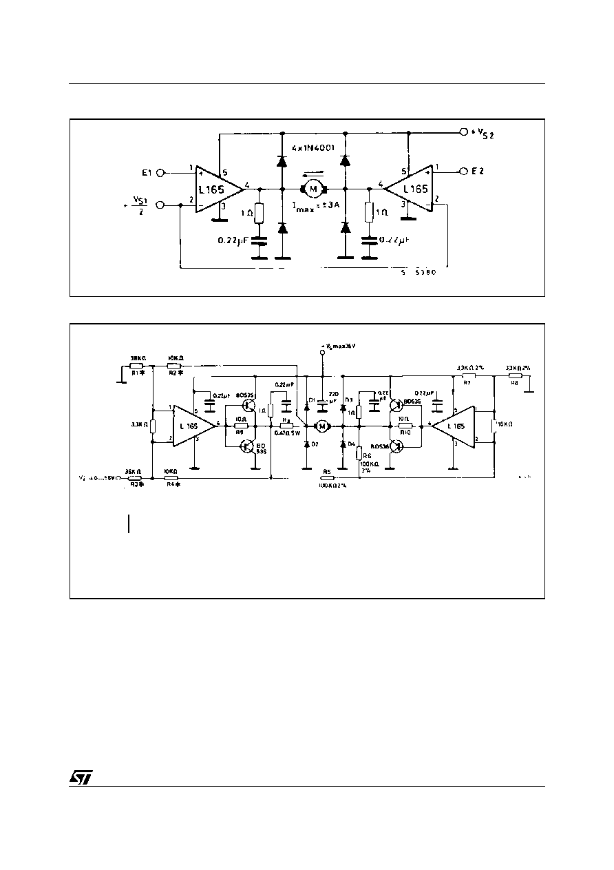
Figure 9. Bidirectional DC motor control with TTL/CMOS/
µ
P compatible inputs.
Figure 10. Motor current control circuit with external power transistors (I
motor
> 3.5A).
Must be V
S2
V
S1
; E1, E2 = logic inputs; V
S1
= logic supply voltage
D1 to D4: V
F
1.2 @ I = 4A
t
rr
500ns
Note : The inputvoltage level is compatible with L291 (5-BIT D/A converter).
The transfer function is:
I
M
V
i
-----
R4
Rx R 3
------------------
=