 | –≠–ª–µ–∫—Ç—Ä–æ–Ω–Ω—ã–π –∫–æ–º–ø–æ–Ω–µ–Ω—Ç: L2726-2 | –°–∫–∞—á–∞—Ç—å:  PDF PDF  ZIP ZIP |
L2726
October 1998
LOW DROP DUAL POWER OPERATIONAL AMPLIFIER
Æ
.
OUTPUT CURRENT TO 1 A
.
OPERATES AT LOW VOLTAGES
.
SINGLE OR SPLIT SUPPLY
.
LARGE COMMON-MODE AND
DIFFERENTIAL MODE RANGE
.
LOW INPUT OFFSET VOLTAGE
.
GROUND COMPATIBLE INPUTS
.
LOW SATURATION VOLTAGE
.
THERMAL SHUTDOWN
.
CLAMP DIODE
DESCRIPTION
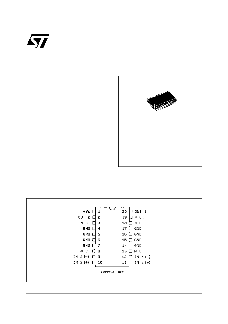
The L2726 is a monolithic integratedcircuit in SO-20
package intended for use as power operational am-
plifiers in a widerangeof applicationsincluding servo
amplifiers and power supplies.
It is particularly indicated for driving inductive loads,
as motor and finds applications in compact-disc
VCR automative, etc.
The high gain and high output power capability pro-
vide superior performance whatever an operational
amplifier/power booster combination is required.
PIN CONNECTION (top view)
SO20
(12 + 4 + 4)
ORDERING NUMBER : L2726
This is advanced information on a new product now in development or undergoing evaluation. Details are subject to change without notice.
1/6
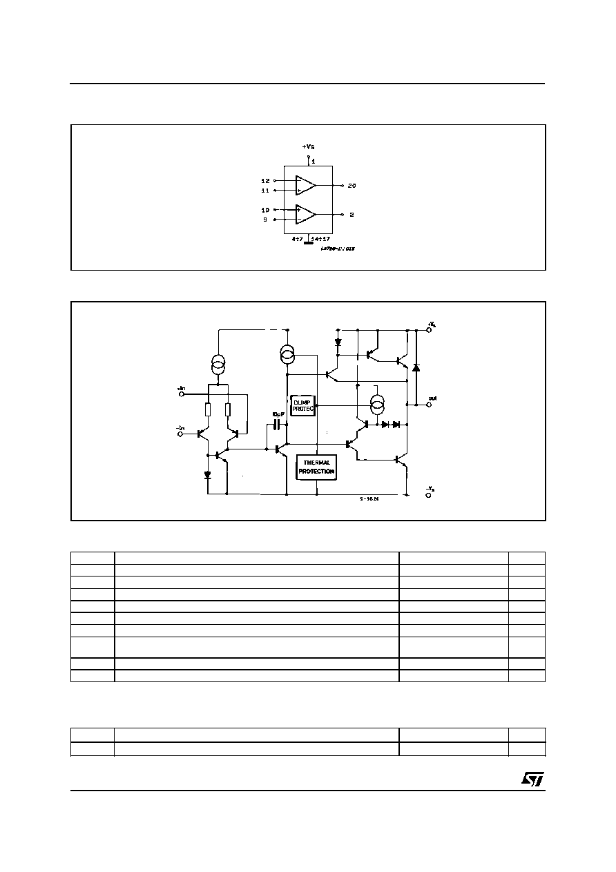
BLOCK DIAGRAM
SCHEMATIC DIAGRAM (one section)
ABSOLUTE MAXIMUM RATINGS
Symbol
Parameter
Value
Unit
V
s
Supply Voltage
28
V
V
s
Peak Supply Voltage (50ms)
50
V
V
i
Input Voltage
V
s
V
i
Differential Input Voltage
±
V
s
I
O
DC Output Current
1
A
I
p
Peak Output Current (non repetitive)
1.5
A
P
tot
Power Dissipation at
T
amb
= 85
o
C
T
case
= 75
o
C
1
5
W
T
op
Operating Temperature
≠ 40 to 85
o
C
T
stg
, T
j
Storage and Junction Temperature
≠ 40 to 150
o
C
THERMAL DATA
R
th j-case
Thermal Resistance Junction-case
Max.
15.0
o
C/W
R
th j-amb
Thermal Resistance Junction-ambient (*)
Max.
65
o
C/W
(*) With 4 sq. cm copper area heatsink.
L2726
2/6

ELECTRICAL CHARACTERISTICS
V
s
= 24V, T
amb
= 25
o
C unless otherwise specified
Symbol
Parameter
Test Conditions
Min.
Typ.
Max.
Unit
V
s
Single Supply Voltage
4
28
V
V
s
Split Supply Voltage
±
2
±
14
V
I
s
Quiescent Drain Current
V
o
=
V
s
2
V
s
= 24V
10
15
mA
V
s
= 24V
9
15
I
b
Input Bias Current
0.2
1
µ
A
V
os
Input Offset Voltage
10
mV
I
os
Input Offset Current
100
nA
SR
Slew Rate
2
V/
µ
s
B
Gain-bandwidth Product
1.2
MHz
R
i
Input Resistance
500
k
G
v
O. L. Voltage Gain
f = 100Hz
f = 1kHz
70
80
60
dB
e
N
Input Noise Voltage
B = 22Hz to 22kHz
10
µ
V
I
N
Input Noise Voltage
200
pA
CMR
Common Mode Rejection
f = 1kHz
66
84
dB
SVR
Supply Voltage Rejection
f = 100Hz
V
s
= 24V
R
G
= 10k
V
s
=
±
12V
V
R
= 0.5V
V
s
=
±
6V
60
70
75
80
dB
dB
dB
V
DROP(HIGH)
V
s
=
±
2.5V to
±
12V
I
p
= 100mA
I
p
= 500mA
0.7
1
1.5
V
V
DROP(LOW)
V
s
=
±
2.5V to
±
12V
I
p
= 100mA
I
p
= 500mA
0.3
0.5
1
V
C
s
Channel Separation
f = 1KHz
V
s
= 24V
R
L
= 10
V
s
= 6V
G
v
= 30dB
60
60
dB
T
sd
Thermal Shutdown Junction
Temperature
150
o
C
Figure 1 : Quiescent Current vs. Supply Voltage
Figure 2 : Open Loop Gain vs. Frequency
L2726
3/6

Figure 3 : Common Mode Rejection Frequency
Figure 4 : Output Swing vs. Load Current
(V
s
=
±
5V)
Figure 5 : Output Swing vs. Load Current
(V
s
=
±
12 V)
Figure 6 : Supply Voltage Rejection vs.
Frequency
Figure 7 : Channel Separation vs. Frequency.
L2726
4/6

1
11
20
A
e
B
D
E
L
K
H
A1
C
SO20MEC
h x 45
SO20
DIM.
mm
inch
MIN.
TYP.
MAX.
MIN.
TYP.
MAX.
A
2.35
2.65
0.093
0.104
A1
0.1
0.3
0.004
0.012
B
0.33
0.51
0.013
0.020
C
0.23
0.32
0.009
0.013
D
12.6
13
0.496
0.512
E
7.4
7.6
0.291
0.299
e
1.27
0.050
H
10
10.65
0.394
0.419
h
0.25
0.75
0.010
0.030
L
0.4
1.27
0.016
0.050
K
0
∞
(min.)8
∞
(max.)
OUTLINE AND
MECHANICAL DATA
10
L2726
5/6