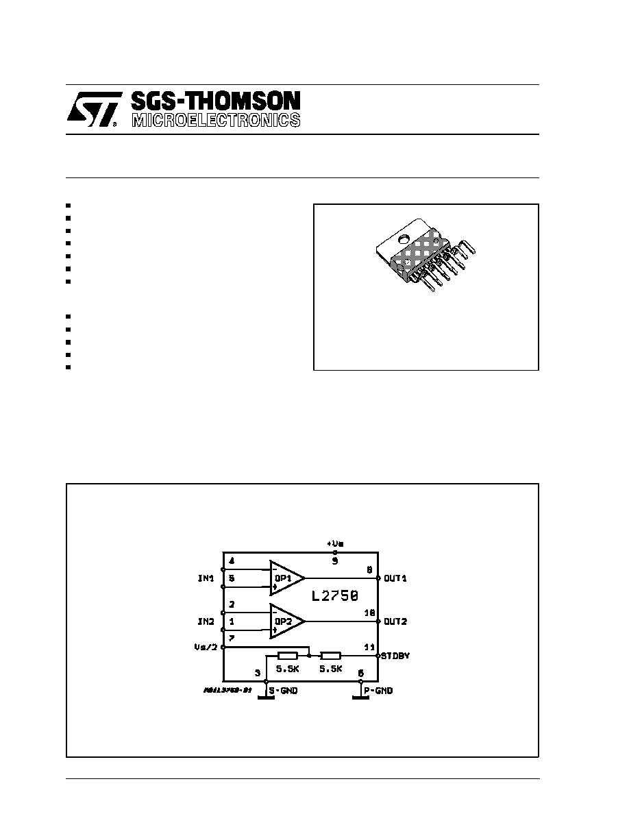
L2750
DUAL LOW DROP HIGH POWER
OPERATIONAL AMPLIFIER
ADVANCE DATA
HIGH OUTPUT CURRENT
VERY LOW SATURATION VOLTAGE
LOW VOLTAGE OPERATION
LOW INPUT OFFSET VOLTAGE
GND COMPATIBLE INPUTS
ST-BY FUNCTION (LOW CONSUMPTION)
HIGH APPLICATION FLEXIBILITY
PROTECTIONS:
VERY INDUCTIVE LOADS
OVERRATING CHIP TEMPERATURE
LOAD DUMP VOLTAGE
FORTUITOUS OPEN GROUND
ESD
DESCRIPTION
The L2750 is a new technology class AB dual
power operational amplifier assembled in Multi-
watt 11 package.
Thanks to the fully complementary PNP/NPN out-
put configuration the L2750 can deliver a rail-to-
rail output voltage swing even at the highest cur-
rent.
Additional feature is the very low current Stand-
By function.
The high application flexibility of the L2750 makes
the device suitable for either motor driving/control
and audio applications purposes.
This is advanced information on a new product now in development or undergoing evaluation. Details are subject to change without notice.
October 1991
BLOCK DIAGRAM
Multiwatt-11
ORDERING NUMBER: L2750
1/10
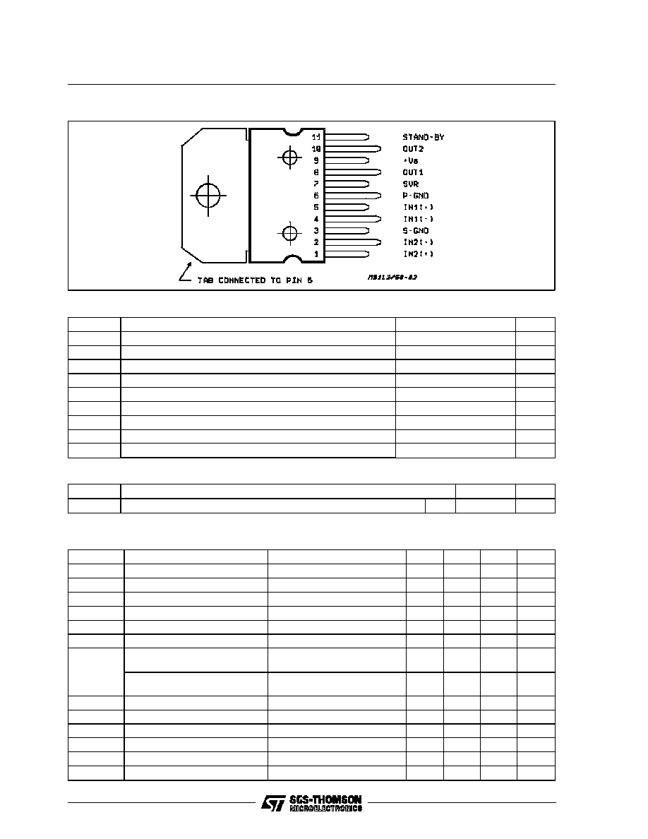
PIN CONNECTION (Top view)
ABSOLUTE MAXIMUM RATINGS
Symbol
Parameter
Value
Unit
V
S op
Operating Supply Voltage
18
V
V
S max
Supply Voltage
28
V
V
PEAK
Peak Supply Voltage (t = 50ms)
40
V
V
i
Input Voltage
V
S op
V
V
i
Differential Input Voltage
V
S op
V
I
O
Output Peak Current (non rep. t = 100
�
s)
5
A
I
O
Output Peak Current (rep. f > 10Hz)
4
A
P
tot
Power Dissipation T
CASE
= 85
�
C
36
W
T
stg
, T
j
Storage and Junction Temperature
-40 to 150
�
C
THERMAL DATA
Symbol
Description
Value
Unit
R
th j-case
Thermal Resistance Junction-case
Max
1.8
�
C/W
ELECTRICAL CHARACTERISTICS (Refer to the operational amplifier with G
V
= 24dB; V
S
= 14.4V;
T
amb
= 25
�
C, unless otherwise specified
Symbol
Parameter
Test Condition
Min.
Typ.
Max.
Unit
V
S
Supply Voltage
4
18
V
I
d
Total Quiescent Drain Current
30
50
mA
V
OS
Input Offset Voltage
5
mV
I
SB
ST-BY Current Consumption
50
�
A
I
S
Input Bias Current
0.5
�
A
I
OS
Input Offset Current
50
nA
V
DROP
Output Voltage Drop (High)
I
O
= 0.5A
I
O
= 3A
0.25
1.1
0.5
2.5
V
V
Output Voltage Drop (Low)
I
O
= 0.5A
I
O
= 3A
0.25
1
0.5
2
V
V
SR
Slew Rate
4
V/
�
s
B
Gain Bandwidth Prod
10
MHz
G
V
Open Loop Voltage Gain
f = 1KHz
85
dB
R
IN
Input Resistance
150
M
E
IN
Input Noise Voltage
R
s
= 0 to 10K
f = 22Hz to 22KHz
3
�
V
CMRR
Common Mode Rejection Ratio
75
90
dB
L2750
2/10

APPLICATION SUGGESTION
The high flexibility makes the L2750 suitable for a
wide range of applications.
Motor Controller
The device can be utilized as a motor controller.
Fig.1 represents a bidirectional DC motor control
suitable for logic driving. In these kinds of applica-
tion it is possible to take advantage of the high
current capability of the L2750 for driving several
types of low impedance motors in a broad range
of applications. Moreover the low drop allows high
start up currents even at lowest supply voltage.
Audio Applications
Another typical utilization of the L2750 concerns
the audio field, as follows:
1) DRIVER FOR BOOSTER : The remarkably low
distortion and noise makes the device proper to
be used as high quality driver for main amplifi-
ers (i.e. car radio boosters). An example is
shown by Fig. 5, where the gain is set to 24 dB
(see also the relevant characteristics).
2) CAR RADIO BOOSTER WITH DIFFERENTIAL
INPUT : Fig. 10 shows an example of car radio
booster, with a gain of 30 dB, that is specially
recommended for active loudspeakers. Among
its main feature is the differential input and sub-
sequent high noise suppression. The typical
output power delivered into a 4
load is 24W
(V
S
= 14.4V; d =10%), as shown by the charac-
teristics enclosed.
ELECTRICAL CHARACTERISTICS (continued)
Symbol
Parameter
Test Condition
Min.
Typ.
Max.
Unit
SVR
Supply Voltage Rejection
R
s
= 0
f = 100Hz
75
90
dB
C
T
Crosstalk
f = 1KHz to 10KHz
80
dB
Figure 1
Figure 2: Low Drop Voltage vs. Output Current
Figure 3: High Drop Voltage vs. Output Current
Figure 4: Open Loop Gain vs. Phase Response
L2750
3/10

Figure 5: Stereo Audio Amplifier Application Circuit
Figure 6: P.C. Board and Components Layout of the Circuit of Figure 5 (1:1 scale)
L2750
4/10
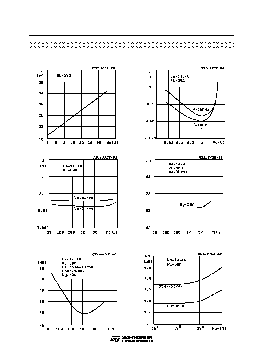
Figure 7: Quiescent Drain Current vs. Supply
Voltage
Figure 11: SupplyVoltage Rejection vs. Frequency
Figure 9: Distortion vs. Frequency
Figure 8: Distortion vs. Output Voltage
Figure 12: E
N
Input vs. R
g
Figure 10: Cross-Talk vs Frequency
AUDIO STEREO APPLICATION CIRCUIT OF FIGURE 5
L2750
5/10