L293D
L293DD
PUSH-PULL FOUR CHANNEL DRIVER WITH DIODES
600mA OUTPUT CURRENT CAPABILITY
PER CHANNEL
1.2A PEAK OUTPUT CURRENT (non repeti-
tive) PER CHANNEL
ENABLE FACILITY
OVERTEMPERATURE PROTECTION
LOGICAL "0" INPUT VOLTAGE UP TO 1.5 V
(HIGH NOISE IMMUNITY)
INTERNAL CLAMP DIODES
DESCRIPTION
The Device is a monolithic integrated high volt-
age, high current four channel driver designed to
accept standard DTL or TTL logic levels and drive
inductive loads (such as relays solenoides, DC
and stepping motors) and switching power tran-
sistors.
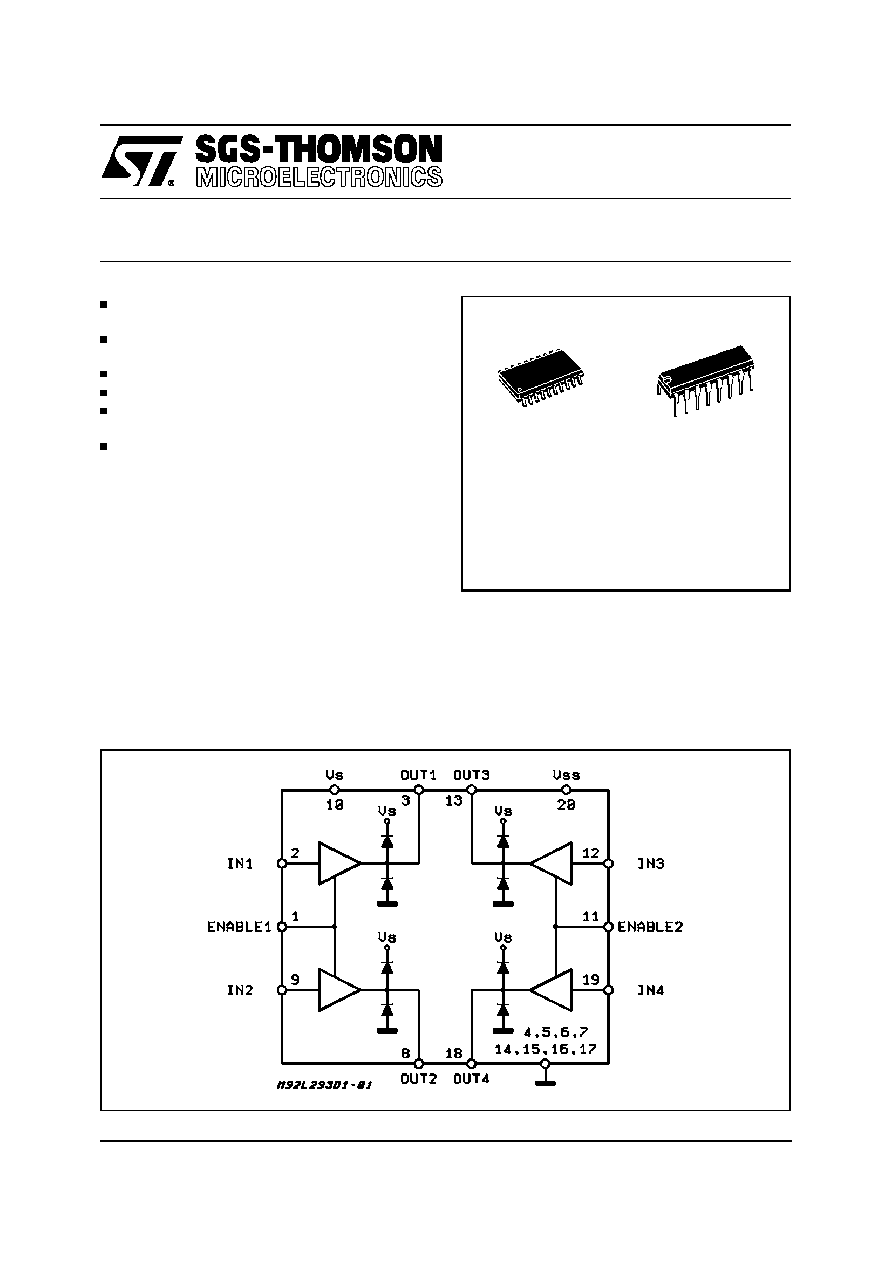
To simplify use as two bridges each pair of chan-
nels is equipped with an enable input. A separate
supply input is provided for the logic, allowing op-
eration at a lower voltage and internal clamp di-
odes are included.
This device is suitable for use in switching appli-
cations at frequencies up to 5 kHz.
The L293D is assembled in a 16 lead plastic
packaage which has 4 center pins connected to-
gether and used for heatsinking
The L293DD is assembled in a 20 lead surface
mount which has 8 center pins connected to-
gether and used for heatsinking.
June 1996
BLOCK DIAGRAM
SO(12+4+4)
Powerdip (12+2+2)
ORDERING NUMBERS:
L293DD
L293D
1/7

ABSOLUTE MAXIMUM RATINGS
Symbol
Parameter
Value
Unit
V
S
Supply Voltage
36
V
V
SS
Logic Supply Voltage
36
V
V
i
Input Voltage
7
V
V
en
Enable Voltage
7
V
I
o
Peak Output Current (100
�
s non repetitive)
1.2
A
P
tot
Total Power Dissipation at T
pins
= 90
�
C
4
W
T
stg
, T
j
Storage and Junction Temperature
� 40 to 150
�
C
THERMAL DATA
Symbol
Decription
DIP
SO
Unit
R
th j-pins
Thermal Resistance Junction-pins
max.
�
14
�
C/W
R
th j-amb
Thermal Resistance junction-ambient
max.
80
50 (*)
�
C/W
R
th j-case
Thermal Resistance Junction-case
max.
14
�
(*) With 6sq. cm on board heatsink.
PIN CONNECTIONS (Top view)
SO(12+4+4)
Powerdip(12+2+2)
L293D - L293DD
2/7

ELECTRICAL CHARACTERISTICS (for each channel, V
S
= 24 V, V
SS
= 5 V, T
amb
= 25
�
C, unless
otherwise specified)
Symbol
Parameter
Test Conditions
Min.
Typ.
Max.
Unit
V
S
Supply Voltage (pin 10)
V
SS
36
V
V
SS
Logic Supply Voltage (pin 20)
4.5
36
V
I
S
Total Quiescent Supply Current
(pin 10)
V
i
= L ; I
O
= 0 ; V
en
= H
2
6
mA
V
i
= H ; I
O
= 0 ; V
en
= H
16
24
mA
V
en
= L
4
mA
I
SS
Total Quiescent Logic Supply
Current (pin 20)
V
i
= L ; I
O
= 0 ; V
en
= H
44
60
mA
V
i
= H ; I
O
= 0 ; V
en
= H
16
22
mA
V
en
= L
16
24
mA
V
IL
Input Low Voltage (pin 2, 9, 12,
19)
� 0.3
1.5
V
V
IH
Input High Voltage (pin 2, 9,
12, 19)
V
SS
7 V
2.3
V
SS
V
V
SS
> 7 V
2.3
7
V
I
IL
Low Voltage Input Current (pin
2, 9, 12, 19)
V
IL
= 1.5 V
� 10
�
A
I
IH
High Voltage Input Current (pin
2, 9, 12, 19)
2.3 V
V
IH
V
SS
� 0.6 V
30
100
�
A
V
en L
Enable Low Voltage
(pin 1, 11)
� 0.3
1.5
V
V
en H
Enable High Voltage
(pin 1, 11)
V
SS
7 V
2.3
V
SS
V
V
SS
> 7 V
2.3
7
V
I
en L
Low Voltage Enable Current
(pin 1, 11)
V
en L
= 1.5 V
� 30
� 100
�
A
I
en H
High Voltage Enable Current
(pin 1, 11)
2.3 V
V
en H
V
SS
� 0.6 V
�
10
�
A
V
CE(sat)H
Source Output Saturation
Voltage (pins 3, 8, 13, 18)
I
O
= � 0.6 A
1.4
1.8
V
V
CE(sat)L
Sink Output Saturation Voltage
(pins 3, 8, 13, 18)
I
O
= + 0.6 A
1.2
1.8
V
V
F
Clamp Diode Forward Voltage
I
O
= 600nA
1.3
V
t
r
Rise Time (*)
0.1 to 0.9 V
O
250
ns
t
f
Fall Time (*)
0.9 to 0.1 V
O
250
ns
t
on
Turn-on Delay (*)
0.5 V
i
to 0.5 V
O
750
ns
t
off
Turn-off Delay (*)
0.5 V
i
to 0.5 V
O
200
ns
(*) See fig. 1.
L293D - L293DD
3/7

TRUTH TABLE (one channel)
Inpu t
Enable (*)
Output
H
L
H
L
H
H
L
L
H
L
Z
Z
Z = High output impedance
(*) Relative to the considered channel
Figure 1: Switching Times
Figure 2: Junction to ambient thermal resistance vs. area on board heatsink (SO12+4+4 package)
L293D - L293DD
4/7