 | –≠–ª–µ–∫—Ç—Ä–æ–Ω–Ω—ã–π –∫–æ–º–ø–æ–Ω–µ–Ω—Ç: L3037FN | –°–∫–∞—á–∞—Ç—å:  PDF PDF  ZIP ZIP |
L3037
SUBSCRIBER LINE INTERFACE CIRCUIT
MONOCHIP SILICON SLIC SUITABLE FOR
PUBLIC/PRIVATE APPLICATIONS
IMPLEMENTS ALL KEY FEATURES OF THE
BORSCHT FUNCTION
SOFT BATTERY REVERSAL WITH PRO-
GRAMMABLE TRANSITION TIME (3 to 100ms)
METERING PULSE INJECTION AND FILTER-
ING WITH MINIMAL COMPONENTS COUNT
(NO TRIMMING REQUIRED).
PROTECTION RESISTOR MISMATCH COM-
PENSATION
ON HOOK TRANSMISSION
LOOP START/GROUND START FEATURE
IND TEMP. RANGE:
-40
∞
C TO +85
∞
C
LOW POWER DISSIPATION IN ALL OPER-
ATING MODES
INTEGRATED
ZERO
CROSSING
RELAY
DRIVER
INTEGRATED (NOISE-LESS) RING TRIP DE-
TECTION
VERY LOW NO. of STD TOLERANCE EX-
TERNAL COMPONENTS
SELECT PART FOR U.S. APPLICATIONS
(63dB TYP. LONG. BALANCE)
SURFACE MOUNT PACKAGE (PLCC44 or
PQFP44)
INTEGRATED THERMAL PROTECTION
PIN TO PIN COMPATIBLE WITH L3035/36
DESCRIPTION
The L3037 subscriber line interface circuit is a bi-
polar device in 70V technology developed for cen-
tral office / loop carrier and private applications.
The L3037 is pin to pin and function compatible
with L3035/36. One particular pin (reserved in
L3035/36) is now used for reverse polarity transi-
tion time programming. The line polarity transition
is not affecting the AC signal transmission that
can continue also during the line voltage transi-
tion.L3037 is available in two different package
options: PLCC44 and PQFP44 (10 x 10mm).
This is advanced information on a new product now in development or undergoing evaluation. Details are subject to change without notice.
December 1997
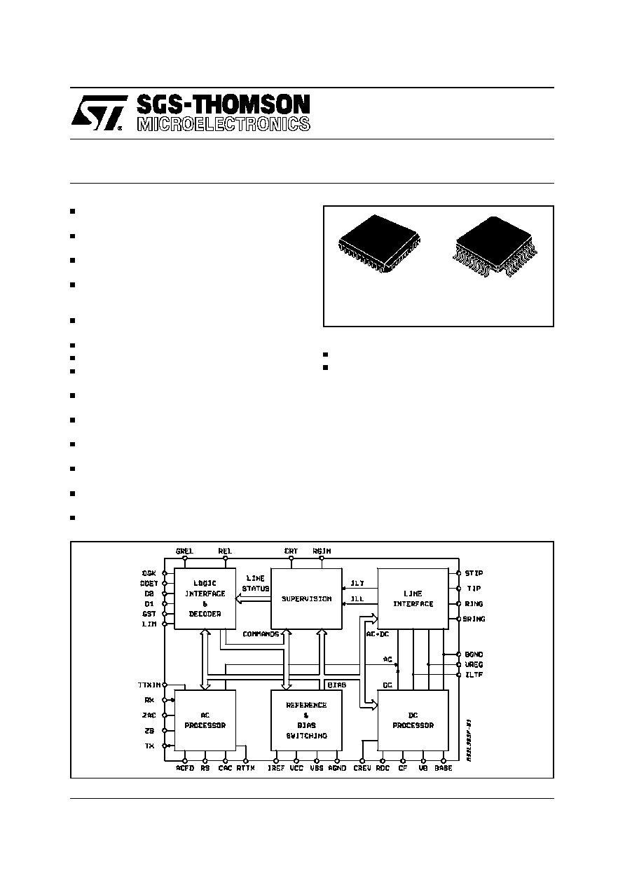
BLOCK DIAGRAM
PLCC44
PQFP44(10 x 10)
ORDERING NUMBERS:
L3037FN
L3037QN
1/22
LINE
STATUS
OGK
ODET
D0
D1
GST
LIM
COMMANDS
ILT
ICRT
VREF
ICRT
0 CROSS
DETECT.
CRT
REL
GREL
RGIN
ILT
ILL
(IA+IB)/200
(IA-IB)/200
1
IA
-1
IB
(IA+IB)/200
AC+DC
AC
SUPPLY
REGULATOR
IREV
DC
REFERENCE
&
BIAS
SWITCHING
1
1
TTXIN
RX
ZAC
ZB
TX
ACFD
RS
CAC
RTTX
IREF
VCC
VSS
AGND
CREV
VB
CF
BASE
RDC
ILTF
VREG
BGND
RING
TIP
SRING
STIP
AC
PROCESSOR
DC
PROCESSOR
LINE
INTERFACE
SUPERVISION
LOGIC
INTERFACE
&
DECODER
+
-
2.32
1
BIAS
D94TL136
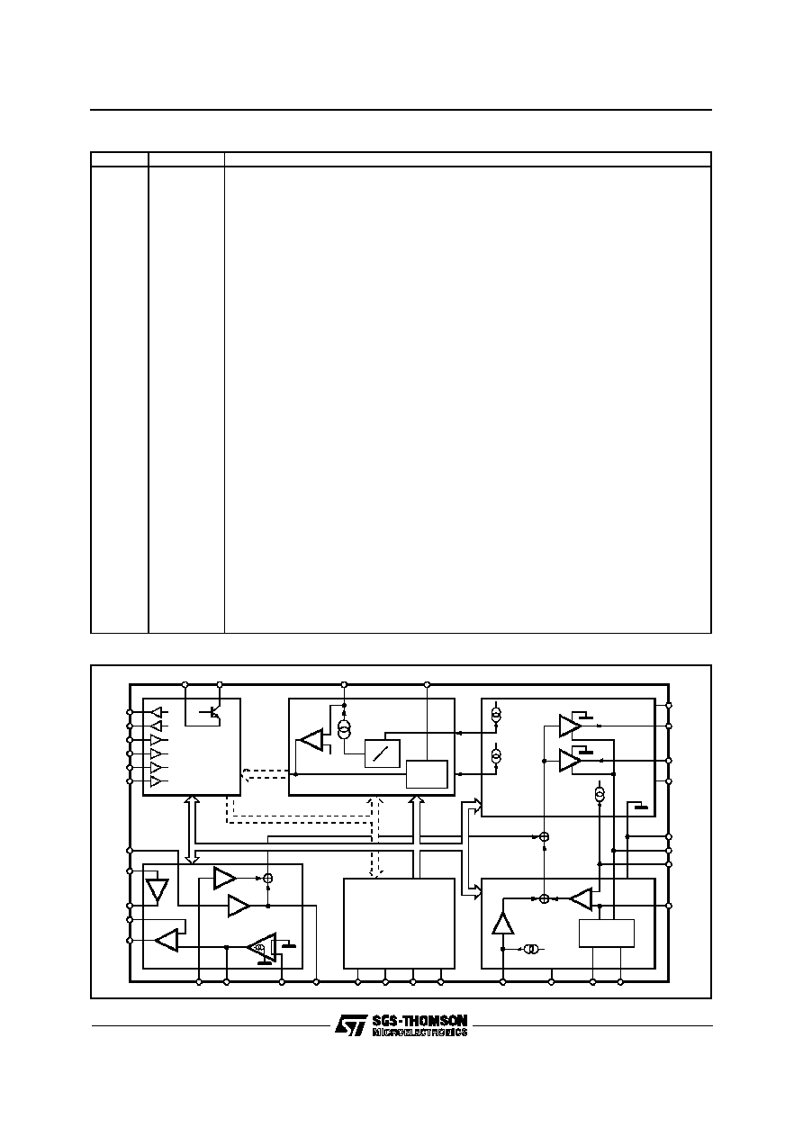
L3037 FUNCTIONAL DIAGRAM
L3037 PIN FUNCTIONALITY (PLCC44)
No.
Name
Function
1
2
3
4
5
6
7
8
9
10 to14
15
16
17
18
19
20
21
22
23
24
25
26
27
28
29
30
31
32 to 36
37
38
39
40
41
42
43
44
V
CC
I
LTF
RDC
CF
BASE
BGND
VREG
STIP
TIP
VB
RING
SRING
CRT
ODET
RGIN
OGK
GST
D1
D0
LIM
V
SS
REL
CREV
GREL
CAC
RS
ZB
VB
Tx
Rx
Z
AC
TTXIN
RTTX
ACFD
AGND
I
REF
Supply input (+5V)
Analog output (current source)
Analog input (current input)
Analog input (voltage input)
Analog output (voltage source)
Ground input (0V)
Supply input (VREG)
Analog input (voltage input)
Analog output (voltage output)
Supply input (-V
BAT
)
Analog output (voltage output)
Analog input (voltage input)
Analog input/output (voltage input / current output)
Digital output (voltage output with internal pull up)
Analog input (current input)
Digital output (voltage output with internal pull up)
Digital input (voltage input, internal pull down)
Digital input (voltage input)
Digital input (voltage input)
Digital input (voltage input 3 levels: 0, +5, open)
Supply input (-5V)
Digital output (voltage output open drain)
Analog input/output (voltage input/current output)
Ground input (0V)
Analog input (current input)
Analog input/output (current output/voltage input)
Analog input (voltage input)
Supply input (-V
BAT
)
Analog output (voltage output)
Analog input (voltage input)
Analog output (voltage output)
Analog input (voltage input)
Analog output (voltage output)
Analog input (voltage input)
Ground input (0V)
Analog input/output (voltage output/current input)
L3037
2/22

PIN CONNECTION (Top view)
ABSOLUTE MAXIMUM RATINGS
Symbol
Parameter
Value
Unit
V
bat
Battery Voltage
-64 to V
SS
+0.5
V
V
CC
Positive Supply Voltage (0 to 1ms)
(continuous)
-0.4 to +7
-0.4 to +5.5
V
V
V
SS
Negative Supply Voltage (0 to 1ms)
(continuous)
-7 to +0.4
-5.5 to +0.4
V
V
V
ag nd
-
V
bgnd
Agnd Respect Bgnd (continuous)
-2 to +2
V
V
REL
Ring Relay Supply Voltage
14
V
V
dig
Digital I/O D0, D1, GST, LIM, ODET, OGK
-0.4 to +5.5
V
I
dig
Digital I/O D0, D1, GST, LIM, ODET, OGK
-3 to +3
mA
T
j
Maximum Junction Temperature
+150
∞
C
T
stg
Storage Temperature
-55 to +150
∞
C
Hu
Humidity
5 to 95
%
Note: In case of power on, power failure or hot insertion with V
DD
, V
SS
present and V
bat
floating the Absolute Maximum Ratings can be exceeded
with Vbat > V
SS
+0.5V. In this case the power consumption of the device increases and the logic output state including relay driver are
not controlled. This effect can be prevented ensuring that Vbat is always present before V
DD
and V
SS
or connecting one shottky diode
(e.g. BAT49X or equivalent) between Vbat and V
SS
. One diode can be shared between all the SLICs of the same line card.
OPERATING RANGE
Symbol
Parameter
Value
Unit
T
op
Operating Temperature Range
-40 to +85
∞
C
V
ag nd
-
V
bgnd
Difference between Agnd and Bgnd
-2 to +2
V
V
CC
Positive Supply voltage
+4.5 to +5.5
V
V
SS
Negative Supply Voltage
-5.5 to -4.5
V
V
bat
Battery Voltage
-62 to -17
V
V
REL
Ring Relay Supply Voltage
4 to 13
V
THERMAL DATA
Symbol
Parameter
PLCC44
PQFP44
Unit
R
th j-amb
Thermal Resistance Junction-ambient
Max.
45
75
∞
C/W
PLCC44
1
2
3
5
6
4
7
8
9
10
17
11
18
19
20
21
22
44
43
42
41
39
40
38
37
36
35
34
28
27
26
24
23
25
33
32
31
29
30
N.C.
N.C.
TIP
VREG
VB
STIP
CRT
N.C.
SRING
N.C.
RING
ODET
RGIN
OGK
GST
D0
D1
LIM
V
SS
REL
CREV
GREL
BGND
BASE
CF
RDC
V
CC
ILTF
IREF
AGND
N.C.
ACFD
RTTX
VB
N.C.
N.C.
RS
CAC
ZB
TTXIN
ZAC
RX
N.C.
TX
D94TL129
12
13
14
15
16
PQFP44
L3037
3/22

PIN DESCRIPTION
Unless otherwise specified all the diagrams in this datasheet refers to the PLCC44 Pin Connection.
PQFP44
No.
PLCC44
No.
Pin
Description
39
1
V
CC
Positive Power Supply (+5V)
40
2
I
LTF
Transversal Line Current Image ((I
A
+ I
B
) / 200)
41
3
RDC
DC feedback input (the RDC resistor is connected from this node to I
LTF
)
42
4
CF
Battery voltage ripple rejection (C
SVR
capacitor is connected from this node to BGND).
43
5
BASE
Driver for external transistor base
44
6
BGND
Battery ground
2
7
VREG
Regulated Voltage. Provides negative power supply for the power amplifier.
(connected to emitter of the external transistor.)
3
8
STIP
Input of A power amplifier (when no compensation of ext. ptc resistor mismatch is
requested it must be shorted to the TIP lead).
4
9
TIP
A line termination output (I
A
is the current sourced from this pin).
1, 28
10 to 14
32 to 36
VB
Battery Supply
PLCC44: All pins are internally connected together.
PQFP44: It is mandatory to short pin 1 and pin 28 as closed as possible to the device.
8
15
RING
B line termination output (I
B
is the current sunk into this pin).
9
16
SRING
Input of B power amplifier (when no compensation of ext. ptc resistor mismatch is
requested it must be shorted to the RING lead).
11
17
CRT
Ring trip and ground key capacitor
12
18
ODET
ON/OFF hook and RING TRIP output (when disable is internally pulled up)
13
19
RGIN
Ring input signal. (when open is internally pulled to GND)
14
20
OGK
Ground key output (when disable is internally pulled up)
15
21
GST
A open command (when open is internally pulled down)
16
22
D1
Bit 1
17
23
D0
Bit 0
18
24
LIM
Current Limitation Program. (when open is internally forced to 44mA current limitation)
19
25
V
SS
Negative Power Supply (-5V)
20
26
REL
Ring relay driver output
21
27
CREV
Reverse polarity transition time control. One proper capacitor connected between this
pin and AGND is setting the reverse polarity transition time. If reverse polarity feature
is not used must be open or connected to AGND through a filter capacitor.
22
28
GREL
Ground reference for ring relay driver
23
29
C
AC
AC feedback input (ACDC split capacitor is connected from this node to ILTF)
24
30
R
S
Protection resistors image (the image resistor is connected from this node to ACFD)
25
31
Z
B
Balance network for 2 to 4 wire conversion (the balance impedance Z
B
is connecetd
from this node to AGND. The Z
A
impedance is connected from this node to Z
AC
)
30
37
Tx
4 wire output port (Tx output)
31
38
Rx
4 wire receiving port. (Rx input)
32
39
Z
AC
Rx buffer output (the AC impedance is connected from this node to ACFD)
33
40
TTXIN
Metering input port/V
drop
programming. If not used should be connected to AGND.
34
41
RTTX
Metering cancellation network. If not used should be left open.
35
42
ACFD
AC impedance synthesis
37
43
AGND
DC and AC signal ground
38
44
I
REF
Voltage Reference Output
2,5 to 7,
10,26,
27, 29,36
≠
N.C.
Not connected
L3037
4/22

DESCRIPTION (continued)
One special selection with high longitudinal balan-
ce performances allows to meet the United States
BELLCORE requirements for central office/loop
carrier and private applications.
The SLIC integrates loop start, ground start,
ground key on/off-hook, automatic ring-trip as well
as zero crossing ring relay driver.
Two to four wire conversion is implemented by the
SLIC for application with first generation COMBO.
In case of application with second generation (pro-
grammable) COMBO this function can be imple-
mented outside saving external components.
The L3037 offers programmable current limitation
(3 ranges), on hook transmission and low power
in all operating modes, power management is
controlled by a simple external low cost transistor.
Metering pulses are injected on the line via a sum-
ming node through TTXIN pin.
Metering pulse filtering is performed by means of a
simple RC network with standard tolerance compo-
nents. In case TTX function is not used this pin
must be connected to AGND. It is also possible to
use this pin to modify the DC voltage drop between
TIP/RING terminals and battery voltage for appica-
tions where it is important to optimize the battery
voltage supply versus the signal swing.
Effect of protection resistors mismatch are com-
pensated by a feedback loop on the final stage al-
lowing good long balance performances also with
large tolerance protection resistors (ex: PTC).
This function allow the L3037 to be fully conform
to BELLCORE power cross and surge test and
meet also the Longitudinal Balance Specification
without using matched PTC resistors.
An integrated thermal protection circuit forces the
L3037 in POWER DOWN (PD) mode when the
junction temperature exceeds 150
∞
C Typ.
The L3037 is specified over -40
∞
C to +85
∞
C am-
bient temperature range.
The L3037 package is a surface mount PLCC44
or PQFP44.
FUNCTIONAL DESCRIPTION
L3037 is designed in 70V bipolar technology and
performs the telephone line interface functions re-
quired in both C.O. and PABX environments. The
full range of signal transmission, battery feed,
loop supervision are performed.
Signal transmission performance is compatible
with European and North American Standards
and with CCITT recommendations.
Ringing, overvoltage and power cross protection
are performed by means of external networks.
The signal transmission function includes both 2
to 4 wire and 4 to 2 wire conversion. The 2W ter-
mination impedance is set by means of an exter-
nal impedance which may be complex. The 2 to 4
wire conversion is provided by means of an exter-
nal network.
Such a network can be avoided in case of appli-
cations with COMBOII, in this case the 2 to 4 wire
conversion is implemented inside the COMBOII
by means of the programmable Hybal filter.
An additional input allows a metering pulse signal
to be added on the line.
The DC feed resistance is programmable with
one external resistor. Three different values of
current limitation (25, 44, 55mA)can be selected
by software through the parallel digital interface.
One external transistor reduces the power dissi-
pation inside the L3037 in the presence of a short
loop (limiting current region).
An additional supervisory function sets the TIP
lead into high impedance state in order to allow
application in ground start configurations.
The different L3037 operating modes are control-
led by a 4bit logic interface, two additional detec-
tor outputs provide ground key detection and ei-
ther hook state or ring trip detection.
SLIC OPERATING MODES
Through the L3037 digital interface it is possible
to select 5 different SLIC operating modes:
1) Active Mode (ACT)
2) Standby Mode (SBY)
3) Tip Open Mode (TO)
4) Power Down Mode (PD)
5) Ringing Mode (RNG)
In both ACT and SBY modes it is possible to se-
lect the reverse polarity (see control interface).
Transition from direct to reverse polarity is soft
and the transition time is defined by the external
capacitor CREV.
ACTIVE MODE (ACT)
This operating mode is set by the card controller
when the Off-Hook condition has been recognized.
When this operating mode is selected the two out-
put buffers (TIP/RING) can sink or source up to
100mA each. In case of Ground key or line termi-
nals to GND the output current is limited to 15mA
for the Tip wire and 30mA for the Ring wire.
As far as the DC characteristic is concerned three
different feeding conditions are present:
a) Current limiting region: the DC impedance of
the SLIC is very high ( 20Kohm) and therefore the
system works like a current source. Using the
L3037 digital interface it is possible to select the
value of the limiting current:
25mA, 44mA, or 55mA.
When the device is in limiting current region the
negative supply for the output buffer is fixed by
L3037
5/22