 | –≠–ª–µ–∫—Ç—Ä–æ–Ω–Ω—ã–π –∫–æ–º–ø–æ–Ω–µ–Ω—Ç: L3121B | –°–∫–∞—á–∞—Ç—å:  PDF PDF  ZIP ZIP |
L3121B
Æ
May 1999 - Ed:4A
PROGRAMMABLE TRANSIENT VOLTAGE
SUPPRESSOR FOR SLIC PROTECTION
SIP4
Application Specific Discretes
A.S.D.
TM
BIDIRECTIONAL FUNCTION WITH VOLTAGE
PROGRAMMABILITY IN BOTH POSITIVE AND
NEGATIVE POLARITIES.
PROGRAMMABLE BREAKDOWN VOLTAGE
UP TO 100 V.
HOLDING CURRENT = 150 mA min.
HIGH SURGE CURRENT CAPABILITY.
I
PP
= 100A , 10/1000
µ
s
FEATURES
This device has been especially designed to pro-
tect a subscriber line interface circuit (SLIC) with
an integrated ring generator.
Used with the recommended application circuit,
each line (TIP and RING) is protected against posi-
tive and negative surges. In the positive polarity,
the breakdown voltage is referenced to the + VB ,
and in the negative polarity, the breakdown voltage
is referenced to the -Vbat .
Its high surge current capability makes the L3121B
a reliable protection device for very exposed equip-
ment, or when series resistors are very low.
DESCRIPTION
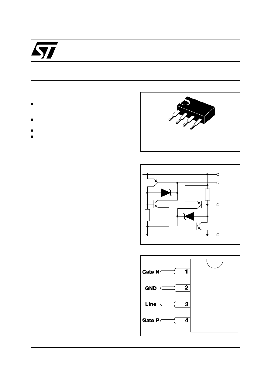
CONNECTION DIAGRAM
Gate N
Gate P
GND
Line
SCHEMATIC DIAGRAM
1/7
COMPLIES WITH THE
FOLLOWING STANDARDS:
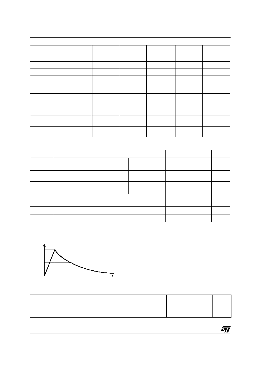
Peak Surge
Voltage
(V)
Voltage
Waveform
(
µ
s)
Current
Waveform
(
µ
s)
Admissible
Ipp
(A)
Necessary
Resistor
(
)
ITU-T K20
4000
10/700
5/310
100
-
VDE0433
4000
10/700
5/310
100
-
VDE0878
4000
1.2/50
1/20
100
-
IEC1000-4-5
level 4
level 4
10/700
1.2/50
5/310
8/20
100
100
-
-
FCC Part 68, lightning surge
type A
1500
800
10/160
10/560
10/160
10/560
200
100
-
-
FCC Part 68, lightning surge
type B
1000
9/720
5/320
25
-
BELLCORE TR-NWT-001089
First level
2500
1000
2/10
10/1000
2/10
10/1000
250
100
-
-
BELLCORE TR-NWT-001089
Second level
5000
2/10
2/10
250
10
Symbol
Parameter
Value
Unit
I
PP
Peak pulse current
10/1000
µ
s
2/10
µ
s
100
250
A
I
TSM
Non repetitive surge peak on-state
current
tp = 10 ms
50
A
V
MLG
V
MGL
Maximum voltage LINE/GND.
Maximum voltage GATE/LINE.
100
80
V
V
T
stg
T
j
Storage temperature range
Maximum operating junction temperature
- 40 to + 150
+ 150
∞
C
∞
C
T
L
Maximum lead temperature for soldering during 10s
260
∞C
Top
Operating temperature range (see note 1)
- 40 to + 85
∞C
Note 1: Variation of electrical parameters is given by curves.
ABSOLUTE MAXIMUM RATINGS (Tamb = 25∞C)
100
50
% IPP
t
t
t
r
p
0
Pulse waveform 10/1000
µ
s
Symbol
Parameter
Value
Unit
R
th (j-a)
Junction-to-ambient
80
∞
C/W
THERMAL RESISTANCE
L3121B
2/7
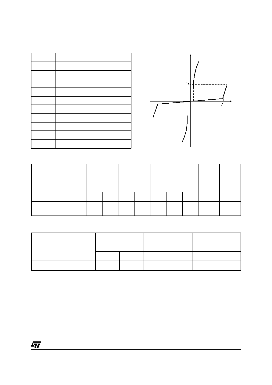
Symbol
Parameter
V
RM
Stand-off voltage
I
RM
Reverse leakage current
V
BR
Breakdown voltage
V
BO
Breakover voltage
I
H
Holding current
I
BO
Breakover current
I
PP
Peak pulse current
V
GN
Gate voltage
I
GN
, I
GP
Triggering gate current
C
Capacitance
ELECTRICAL CHARACTERISTICS (T
amb
= 25 ∞C)
I
I
BO
I
H
V
RM
V
BR
V
BO
I
PP
Type
I
RM
@ V
RM
V
BR
@ I
R
V
BO
@ I
BO
I
H
C
max.
min.
max.
typ.
max.
min.
max.
note 1
note 1
note 2
µ
A
V
V
mA
V
mA
mA
mA
pF
L3121B
5
8
60
90
100
1
180
200
500 150
200
1- OPERATION WITHOUT GATE
Type
V
GN
@ I
GN
= 200mA
I
GN
@ V
AC
= 60V
I
GP
@ V
AC
= 60V
min.
max.
min.
max.
max.
V
V
mA
mA
mA
L3121B
0.6
1.8
80
200
180
2- OPERATION WITH GATE
Note 1 :See the reference test circuits for IH, IBO and VBO parameters.
Note 2 :VR = 5 V, F = 1MHz.
L3121B
3/7

REFERENCE TEST CIRCUIT FOR I
BO
and V
BO
parameters :
220V
static
relay.
R1
R2
240
140
D.U.T
V BO
measure
I
, I
BO
H
measure
t p = 20ms
K
Transformer
220V/800V
5A
Auto
Transformer
220V/2A
Vout
FUNCTIONAL HOLDING CURRENT (I
H
) TEST CIRCUIT = GO - NOGO TEST.
R
- V
P
V
BAT
= - 48 V
Surge generator
D.U.T.
This is a GO-NOGO Test which allows to confirm the holding current (I
H
) level in a functional test circuit.
This test can be performed if the reference test circuit can't be implemented.
TEST PROCEDURE :
1) Adjust the current level at the IH value by short circuiting the line and GND pins of the D.U.T.
2) Fire the D.U.T with a surge Current : Ipp = 10A , 10/1000
µ
s.
3) The D.U.T will come back to the OFF-State within a duration of 50 ms max.
TEST PROCEDURE :
Pulse Test duration (tp = 20ms):
- For Bidirectional devices = Switch K is closed
- For Unidirectional devices = Switch K is open.
V
OUT
Selection
- Device with V
BO
<
200 Volt
- V
OUT
= 250 V
RMS
, R
1
= 140
.
- Device with V
BO
200 Volt
- V
OUT
= 480 V
RMS
, R
2
= 240
.
L3121B
4/7
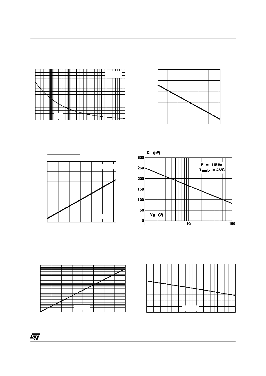
1E-2
1E-1
1E+0
1E+1
1E+2
1E+3
0
5
10
15
20
25
30
35
40
I
(A)
TSM
t(s)
F=50Hz
Tj initial=25∞C
Fig. 1: Surge peak current versus overload
duration (typical values).
0.90
0.94
0.98
1.02
1.06
2.00
2.04
V
[T
]
V
[T
= 25∞C]
BR
amb
BR
amb
-40
-20
0
20
40
60
80
T
(∞C)
amb
I = 1 mA
R
85
Fig. 3: Typical relative variation of breakdown
voltage versus ambient temperature.
Fig. 4: Junction capacitance versus reverse
applied voltage.
-40
-20
0
20
40
60
80 85
0.70
0.85
1.0
1.15
1.30
1.45
I [T
]
I [T
= 25∞C]
H
amb
H
amb
T
(∞C)
amb
Fig. 2: Typical relative variation of holding current
versus ambient temperature.
25
50
75
100
125
1E+0
1E+1
1E+2
1E+3
1E+4
1E+5
Tj(∞C)
IR[Tj] / IR [Tj=25∞C]
Fig. 5: Typical relative variation of leakage current
versus ambient temperature.
-40 -30 -20 -10
0
10 20 30 40 50 60 70 80
0.90
0.95
1.00
1.05
1.10
Tamb(∞C)
Ipp[Tamb] / Ipp [25∞C]
Fig. 6: Typical relative variation of peak pulse
current (10/1000
µ
s) versus ambient temperature.
L3121B
5/7

Typical Slic Protection Concept.
GND
GND
LINE
SLIC
L3000N
-Vbat
-Vbat
+VB
+VB
TIP
RING
L3121B
L3121B
GN
GN
G P
G P
R1
R4
R3
R2
LINE
220nF
220nF
MARKING : Logo, Date Code, Part Number
ORDER CODE
L3121B
DEVICE CODE
L3121B
6/7
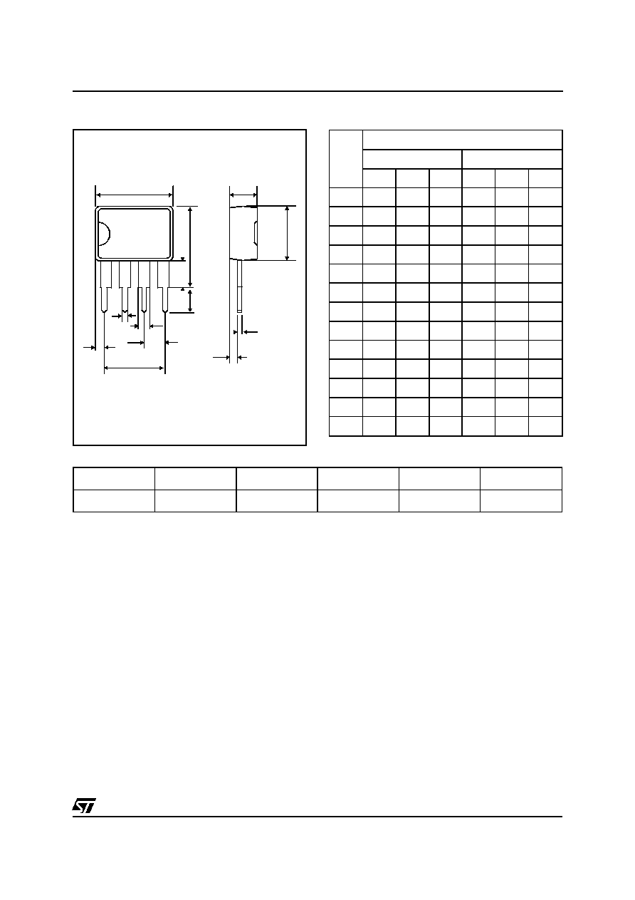
PACKAGE MECHANICAL DATA
SIP4 (Plastic)
Information furnished is believed to be accurate and reliable. However, STMicroelectronics assumes no responsibility for the consequences of
use of such information nor for any infringement of patents or other rights of third parties which may result from its use. No license is granted by
implication or otherwise under any patent or patent rights of STMicroelectronics. Specifications mentioned in this publication are subject to
change without notice. This publication supersedes and replaces all information previously supplied.
STMicroelectronics products are not authorized for use as critical components in life support devices or systems without express written ap-
proval of STMicroelectronics.
The ST logo is a registered trademark of STMicroelectronics
© 1999 STMicroelectronics - Printed in Italy - All rights reserved.
STMicroelectronics GROUP OF COMPANIES
Australia - Brazil - Canada - China - France - Germany - Italy - Japan - Korea - Malaysia - Malta - Mexico - Morocco -
The Netherlands - Singapore - Spain - Sweden - Switzerland - Taiwan - Thailand - United Kingdom - U.S.A.
http://www.st.com
REF.
DIMENSIONS
Millimetres
Inches
Min.
Typ.
Max.
Min.
Typ.
Max.
A
7.10
0.280
a1
2.80
0.110
B
10.15
0.400
b1
0.50
0.020
b2
1.35
1.75 0.053
0.069
C
3.18
3.43 0.125
0.135
c1
0.38
0.50 0.015
0.020
c2
1.30
0.051
e
2.54
0.100
e3
7.62
0.200
I
10.50
0.413
L
3.30
0.130
Z
1.50
0.059
B
I
e
L
b1
e3
c1
A
a1
b2
Z
C
c2
Ordre code
Marking
Package
Weight
Base qty
Delivery mode
L3121B
SIP4
0.55 g
L3121B
7/7