 | –≠–ª–µ–∫—Ç—Ä–æ–Ω–Ω—ã–π –∫–æ–º–ø–æ–Ω–µ–Ω—Ç: L482D1 | –°–∫–∞—á–∞—Ç—å:  PDF PDF  ZIP ZIP |

L482
November 1991
HALL≠EFFECT PICKUP IGNITION CONTROLLER
.
DIRECT DRIVING OF THE EXTERNAL PO-
WER DARLINGTON
.
COIL CURRENT CHARGING ANGLE (DWELL)
CONTROL
.
COIL CURRENT PEAK VALUE LIMITATION
.
CONTINUOUS COIL CURRENT PROTECTION
.
CONDUCTION AND DESATURATION TIME
OUTPUT SIGNALS
.
PERMANENT CONDUCTION PROTECTION
RESET OUTPUT SIGNAL
.
OVERVOLTAGE PROTECTION FOR EXTER-
NAL DARLINGTON
.
LOAD DUMP PROTECTION
DESCRIPTION
The L482 is an integrated circuit designed for use
with an NPN darlington in breakerless ignition sy-
stems with hall-effect pickup sensors and high ener-
gy ignition coils.
It controls the energy stored in the ignition coil and
the desaturation time of the external darlington to
limit the power dissipation.
DIP16
ORDERING NUMBERS : L482 (DIP16)
L482D1 (SO16)
PIN CONNECTIONS (top views)
DIP16
SO16
The L482 is also particularly suitable for use as igni-
tion control and driving stage in more sophisticated
car electronic systems which employ microproces-
sor circuits.
SO16
1/11

BLOCK DIAGRAM
(*) Thermal resistance junction-aluminia with the device soldered on the middle of an aluminia supporting substrate measuring 15 x 20mm ;
0.65mm thickness with infinite heatsink.
ABSOLUTE MAXIMUM RATINGS
Symbol
Parameter
Value
Unit
V
R
Reverse Battery Voltage
≠ 14
V
V
D
Dump Voltage
100
V
P
to t
Power Dissipation at T
amb
= 90
∞
C
SO16
DIP
1.2
0.65
W
W
T
j
, T
stg
Junction and Storage Temperature Range
≠ 55 to 150
∞
C
THERMAL DATA
Symbol
Parameter
Value
Unit
R
th j-amb
Thermal Resistance Junction-ambient (DIP16)
Max
90
∞
C/W
R
th j-al
Thermal Resistance Junction-alumina (SO16)
Max
50
∞
C/W
L482
2/11
PIN FUNCTIONS (refer to fig. 3 for DIP16 package)
N
∞
Name
Function
1
CONDUCTION TIME
SIGNAL
A low level on this output signal indicates when the external darlington is in
the ON condition i.e. when the current flows through the coil (ton in fig.1)
2
HALL-EFFECT INPUT
Hall-effect Pickup Input. A high level on this pin enables the current driving
into the coil. The effective coil charge will be a function of the dwell control
logic. A High to Low transition from the Hall-effect pickup is the signal for
ignition actuation. The input signal, supplied by the open collector output
stage of the Hall-effect sensor, has a duty cycle typically about 70%.
3
DWELL CONTROL
The average voltage on the capacitor C
2
connected between this pin and
ground depends on the motor speed and the voltage supply. The
comparison between V
C2
and V
C5
voltages determines the timing for the
dwell control. The recommended value is 100nF using a 100K
resistor at
pin 7. For the optimized operation of the device, C2 = C5.
4
DWELL CONTROL TIMER
The capacitor C5 connected between this pin and ground is charged when
the Hall-effect output is high and is discharged at the High to Low transition
of the Hall-effect signal. The recommended value is 100nF using a 100K
resistor at pin 7.
5
HALL SENSOR SUPPLY
This pin can be used to project the Hall-effect pickup against the voltage
transients, The resistor R
a
limits the current into the internal zener.
6
DESATURATION TIME
SIGNAL
Open Collector Output Signal. This output is high when the external
darlington is in desaturation condition (current limitation), see t
d
pulse in fig.
1.
7
REFERENCE VOLTAGE
A resistor R11 connected between this pin and ground sets the internal
current used to drive the external capacitors of the dwell control (C
2
and
C
5
) and permanent conduction protection (C
1
). The recommended value is
100K
.
8
PERMANENT CONDUCT.
PROTECTION TIMER
A capacitor C1 connected between this pin and ground determines the
intervention delay of the permanent conduction protection, t
pc
of the figure 2.
With a 1
µ
F capacitor and 100K
resistor R
11
at pin 7 the typical delay is 1s.
9
PERMANENT CONDUCT.
RESET OUTPUT
(no available in
Micropackage) (*)
A low pulse on this output detects the intervention of the permanent
conduction protection, as shown in figure 2. Typically the duration of the
time t
r
is more than 100
µ
s.
10
CURRENT SENSING
INPUT (*)
Connection for Coil Current Limitation. The current is measured on the
sense resistor R
S
and divided on R
1
/R
2
. The current limitation value is
given by :
I
SENS
=
V
SENS
R1
+
R2
R
S
R2
11
DUMP PROTECTION
(*)
The device is protected against the load dump. In load dump condition an
internal circuit,
based on a zener diode and a darlington transistor,
switches off the external darlington and short circuits the supply.
By means of the external divider R8/R9 the protection threshold can be
changed and is given as first approximation by:
V
Dth
=
8.5
R
8
+
R
9
R
9
+
5
10
-
4
R
8
(the resistor R9 value must be higher than 4K
).
12
POWER SUPPLY (*)
Supply Voltage Input. A 7V (typ) zener is present at the input. The external
resistor R
7
limits the current through the Zener for high supply voltages.
L482
3/11

(*) These pins refer only to the DIP package type.
For the SO 16 version the permanent conduction reset output signal is not available and the pin 9 becomes the current sensing input. Pin 10
replaces the pin 11 function, pin 11 becomes the power supply input and pin 12 is used as the signal ground.
ELECTRICAL CHARACTERISTICS (V
S
= 14 V, ≠ 40
∞
C
T
j
125
∞
C referred to application circuit of
figure 3 regarding DIP-16 package version)
Symbol
Parameter
Test Conditions
Min.
Typ.
Max.
Unit
V
S
Operating Supply Voltage
6
28
V
I
S
Supply Current
V
12
= 4.5V
25
mA
V
Z
Zener Voltage (pin 12)
I
Z
= 80mA
6.5
8.8
V
V
I
Sensor Input (pin 2)
LOW Voltage
HIGH
2.5
0.5
V
V
I
I
Sensor Input Current (pin 2)
V
I
= LOW
V
S
= 6 to 16V
≠12
≠1
mA
V
Hz
Hall-cell Supply Zener Voltage
(pin5)
I
Hz
= 10mA
19
22
25
V
I
HZ
Hall-cell Supply Zener Current
(pin5)
t = 10ms
T
AMB
= 25
∞
C
100
mA
V
CE sat
(V
14
≠V
16
)
Series
Darlington Driver Sat.
Voltage
I
o
= 70mA
I
o
= 150mA
0.4
0.6
1.0
V
V
V
SENS
Current Limit. Sensing Voltage
(pin10)
V
S
= 6 to 16V
200
400
mV
I
3D
I
3C
I
3C
/I
3D
C2 Discharge Current
C2 Charge Current
V
S
= 6 to 16V
(*) Note 1
0.2
5
6
3.4
20
35
µ
A
µ
A
V
OVZ
External Darlington Overvoltage
Protection Zener Voltage
I
OVZ
= 5mA to 15mA
T
AMB
= 25
∞
C
25
30
35
V
V
7
Reference Voltage
2.5
3.5
V
t
d
Desaturation Time
f = 40Hz V
S
= 14V
0.6
1.2
1.57
ms
PIN FUNCTIONS (continued)
N
∞
Name
Function
13
GROUND
This pin must be connected to ground.
14
DRIVER COLLECTOR
The collector current for the internal driver which drives the external
darlington is supplied through this pin. The external resistor R
10
limits the
dissipation in the IC. The value of the resistor depends is a function of the
darlington used and on the limiting current in the coil.
15
OVERVOLTAGE
LIMITATION
The external is protected against overvoltage by means of an internal
zener available at this pin. The external divider R
5
/R
6
defines the limitation
value, given as first approximation by:
V
ovp
=
30
R
5
+
5
10
-
3
R
6
+
30
16
DRIVING STAGE
OUTPUT
Current Driver for the External Darlington. To ensure stability and precision
of Tdesat C
3
and R
3
must be used. Recommended value for R3 is 2K
in
order not to change the open loop gain of the system.
R
C
may be added to C
3
to obtain greater flexibility in various application
situations.
C
3
and RC values ranges are 1 to 100nF and 5 to 30K
depending on the
external darlington type.
L482
4/11
ELECTRICAL CHARACTERISTICS (Continued)
Symbol
Parameter
Test Conditions
Min.
Typ.
Max.
Unit
t
PC
Permanent
Conduction
Protection Time (pin 8) (see fig.
2)
V
I
= H
C
I
= 1
µ
F
1
3
5
s
V
1
Charging Angle Output Voltage
LOW
HIGH
I
SINK
= 0
I
SINK
= 1mA
I
SOURCE
= 1.5mA
I
SOURCE
= 2.5mA
3
5
0.5
1.2
V
V
V
V
V
6
Desat.
Time
Output
Low
Voltage
I
6 (sink)
= 0.5mA
0.7
V
I
6L
Desat. Time Leakage Current
(pin6)
V
6
= 5V
10.5
µ
A
I
9L
Permanent
Conduction
Reset
Leakage Current (pin9)
V
9
= 5V
10.5
µ
A
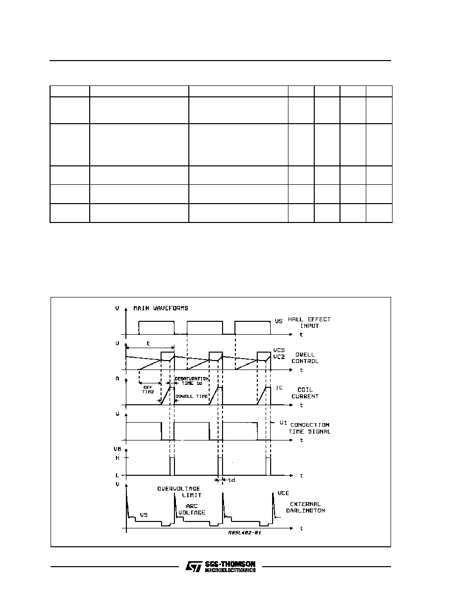
Figure 1 : Main Waveforms.
APPLICATION INFORMATION
L482
5/11

Figure 2 : Low Frequency Condition and Permanent Conduction Protection.
Figure 3 : Application circuit (DIP≠ 16).
L482
6/11

Figure 4 : Application Circuit (SO≠16).
CIRCUIT OPERATION
The L482control the conduction time (dwell) and the
peak value of the primary current in the coil over the
full range of operating conditions.
The coil current is limited to a predetermined level
by means of a negative feedback circuit including a
current sensing resistor, a comparator, the driver
stage and the power switch.
The dwell control circuit maintains the output stage
in its active region during current limitation. The time
the output stage is in the active region (desaturation
time) is sufficient to compensate for possible varia-
tions in the nergy stored due to the acceleration of
the motor ; moreover this time is limited to avoid ex-
cessive power dissipation.
CONTROL OF THE DWELL ANGLE (fig. 1 and 4)
The dwell angle control circuit calculates the con-
duction time D for the output transistor in relation to
the speed of rotation, to the supply voltage and to
the characteristic of the coil.
On the negative edge of the Hall-effect input signal
the capacitor C
2
begins discharging with a constant
current I
3D
. When the set peak value of the coil cur-
rent is reached, this capacitor charges with a con-
stant current I
3C
= 13.3 x I
3D
and the coil current is
kept constant by desaturating the driver stage and
the external darlington.
The capacitor C
5
starts charging on the positive
edge of the Hall-effect input signal with a constant
current I
4C
.
The dwell angle, and consequentlythe starting point
of the coil current production, is decided by the com-
parison between V
C2
and V
C5
. A positive hysteresis
is added to the dwell comparator to avoid spurious
effects and C
5
is rapidly discharged on the negative
edge of Hall-effects input signal.
In this way the average voltage on C
2
increases if
the motor speed decreases and viceversa in order
to maintain constant the ratiotd at any motor speed.
T
td is kept constant (and not d = cost) to control the
power dissipation and to have sufficient time to
avoid low energy sparks during acceleration.
The charging time D ≠ td depends on the coil and
the voltage supply.
DESATURATION TIMES IN STATIC CONDI-
TIONS.In static conditions, if C
2
= C
5
as recommen-
ded and if the values of the application circuit of fig.
3, 4 are used.
td
1
=
T
1 + I
3C
/I
3D
L482
7/11

DESATURATION TIMES IN LOW AND HIGH FRE-
QUENCY OPERATION.Due to the upper limit of the
voltage range of pin 3, if the components of fig. 3, 4
are used, below 10Hz (300RPM for a 4 cylinder en-
gine) the OFF time reaches its maximum value
(about50ms) and then the circuit graduallyloses the
control of the dwell angle because D = T ≠ 50ms
Over 200Hz (6000RPM for a 4 cylinder engine) the
available time for the conduction is less than 3.5ms.
If the used coil is 6mH, 6A, the OFF time is reduced
to zero and the circuit loses the dwell angle control.
TRANSIENT RESPONSE. The ignition system
must deliver constant energy even during the con-
dition of acceleration and deceleration of the motor
below 80Hz/s. These conditions can be simulated
by means of a signal generator with a linearly mo-
dulated frequency between 1Hz and 200Hz (this
correspondsto a change between 30 and 6000RPM
for a 4 cylinders engine.
CURRENT LIMIT. The current in the coil is monito-
red by measuring the I
sense
current flowing in the
sensingresistor R
s
on the emitter of the externaldar-
lington. I
sense
is given by :
I
sense
= I
coil
+ I
16
When the voltage drop across R
s
reaches the inter-
nal comparator threshold value the feedbackloop is
activated and I
sense
kept constant (fig. 1) forcing the
external darlington in the active region. In this con-
dition :
I
sense
= I
coil
When a precise peak coil current is required R
5
must
be trimmed or an auxiliary resistor divider (R
1
, R
2
)
added :
V
SENS
R
1
Icpeak (A)
=
(
+ 1)
R
S
R
2
PROTECTION CIRCUIT
PERMANENT CONDUCTION PROTECTION
The battery voltage is applied to ignition module by
means of the ignition key. In these conditions, with
the motor stopped, it is necessary that there is no
permanent conduction in the ignition coil irrespecti-
ve of the polarity of the input signal.
The L482 incorporates a timing circuit to implement
this protection ; the duration of the intervention is set
by means of a capacitor C
1
at pin 8 = 1
µ
F, and
R
11
= 100k
, when the input signal is high for more
than 1 s, the coil current gradually decreases down
to zero to avoid spurious sparks (see fig. 2).
This timing allows normal operation of the module
above 30RPM.
DARLINGTON OVERVOLTAGE LIMITATION
The darlington is protected against overvoltage by
means of an external divider R
5
/R
6
(pin 15) and an
internal zener. This zener drives the external darlin-
gton in order to limit the collector voltage.
REVERSE BATTERY PRTOTECTION. Due to the
presence of external impedance at pin 5, 10, 11, 14,
15, L482 is protected against reverse battery volt-
age.
DUMP PROTECTION.
The load dump protection withstands up to 100V
with a decay time
300ms. The intervention thre-
shold for load dump is fixed by means of an external
divider connected to pin 11 (DIP-16 package ver-
sion) or to pin 10 using a Micropackage type.
NEGATIVE SPIKE PROTECTION.If correct opera-
tion is requested also during short negative spikes,
the diode DS and capacitor C
s
must be used.
USE OF THE IC ELECTRONIC ADVANCE SY-
STEM
When the device is digitally controlled the control
unit transmits a suitable input signal to the power
module, receiving in turn information that allows the
control of the dwell and the on time of the final tran-
sistor.
For this reason L482 provides the following outputs:
.
a time signal equal to the time in which the final
Darlington is in the active region i.e. when the coil
current is limited (V
ds
) as shown in figure 1. This
signal must be TTL compatible.
.
a TTL compatible output from the timing circuit
(V
rs
in figure 2). This pulse, available only using
the DIP-16 package version is present after the
protection against cranking transients.
.
a time signal equal to the time in which the final
Darlington, is in "on" condition (V
on
) i.e. when the
current flows through the coil, see fig. 1.
OTHER APPLICATION INFORMATION
If the supply voltage is disconnected - or the battery
wire is broken - while the current is flowing through
the coil, the external diode D
1
keeps the coil current
from recirculating into the device : in this way both
device and darlington are protected.
L482
8/11

DIP16 PACKAGE MECHANICAL DATA
DIM.
mm
inch
MIN.
TYP.
MAX.
MIN.
TYP.
MAX.
a1
0.51
0.020
B
0.77
1.65
0.030
0.065
b
0.5
0.020
b1
0.25
0.010
D
20
0.787
E
8.5
0.335
e
2.54
0.100
e3
17.78
0.700
F
7.1
0.280
I
5.1
0.201
L
3.3
0.130
Z
1.27
0.050
L482
9/11

SO16 PACKAGE MECHANICAL DATA
DIM.
mm
inch
MIN.
TYP.
MAX.
MIN.
TYP.
MAX.
A
1.75
0.069
a1
0.1
0.2
0.004
0.008
a2
1.6
0.063
b
0.35
0.46
0.014
0.018
b1
0.19
0.25
0.007
0.010
C
0.5
0.020
c1
45
∞
(typ.)
D
9.8
10
0.386
0.394
E
5.8
6.2
0.228
0.244
e
1.27
0.050
e3
8.89
0.350
F
3.8
4.0
0.150
0.157
L
0.5
1.27
0.020
0.050
M
0.62
0.024
S
8
∞
(max.)
L482
10/11

Information furnished is believed to be accurate and reliable. However, SGS-THOMSON Microelectronics assumes no responsibility for
the consequences of use of such information nor for any infringement of patents or other rights of third parties which may result from its
use. No license is granted by implication or otherwise under any patent or patent rights of SGS-THOMSON Microelectronics. Specifica-
tions mentioned in this publication are subject to change without notice. This publication supersedes and replaces all information pre-
viously supplied. SGS-THOMSON Microelectronics products are not authorized for use as critical components in life support devices or
systems without express written approval of SGS-THOMSON Microelectronics.
©
1994 SGS-THOMSON Microelectronics - All Rights Reserved
SGS-THOMSON Microelectronics GROUP OF COMPANIES
Australia - Brazil - France - Germany - Hong Kong - Italy - Japan - Korea - Malaysia - Malta - Morocco - The Netherlands - Singapore -
Spain - Sweden - Switzerland - Taiwan - Thaliand - United Kingdom - U.S.A.
L482
11/11