 | –≠–ª–µ–∫—Ç—Ä–æ–Ω–Ω—ã–π –∫–æ–º–ø–æ–Ω–µ–Ω—Ç: L4902A | –°–∫–∞—á–∞—Ç—å:  PDF PDF  ZIP ZIP |
L4902A
DUAL 5V REGULATOR WITH RESET AND DISABLE
June 2000
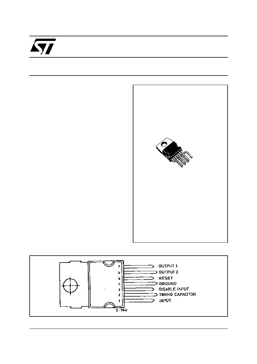
PIN CONNECTION
HEPTAWATT (Vertical)
ORDERING NUMBER : L4902A
Æ
.
DOUBLE BATTERY OPERATING
.
OUTPUT CURRENTS : I
01
= 300 mA
I
02
= 300 mA
.
FIXED PRECISION OUTPUT VOLTAGE
5 V
±
2
%
.
RESET FUNCTION CONTROLLED BY INPUT
VOLTAGE AND OUTPUT 1 VOLTAGE
.
RESET
FUNCTION
EXTERNALLY
PRO-
GRAMMABLE TIMING
.
RESET OUTPUT LEVEL RELATED TO OUT-
PUT 2
.
OUTPUT 2 INTERNALLY SWITCHED WITH
ACTIVE DISCHARGING
.
OUTPUT 2 DISABLE LOGICAL INPUT
.
LOW LEAKAGE CURRENT, LESS THAN 1
µ
A
AT OUTPUT 1
.
RESET OUTPUT NORMALLY HIGH
.
INPUT OVERVOLTAGE PROTECTION UP TO
60V
.
OUTPUT TRANSISTORS SOA PROTECTION
.
SHORT CIRCUIT AND THERMAL OVER-
LOAD PROTECTION
DESCRIPTION
The L4902A is a monolithic low drop dual 5V
regulator designed mainly for supplying microproc-
essor systems.
Reset and data save functions and remote switch
on/off control can be realized.
1/9

BLOCK DIAGRAM
SCHEMATIC DIAGRAM
PIN FUNCTIONS
N
∞
Name
Function
1
Input 1
Regulators Common Input
2
Timing
Capacitor
If Reg. 2 is switched-ON the delay capacitor is charged with a 5
µ
A constant current. When
Reg. 2 is switched-OFF the delay capacitor is discharged.
3
Disable Input
A high level (> V
DT
) disable output Reg. 2.
4
GND
Common Ground
5
Reset Output
When pin 2 reaches 5V the reset output is switched high.
Therefore t
RD
= C
t
(
5V
10
µ
A
) ; t
RD
(ms) = C
t
(nF)
6
Output 2
5V ≠ 300mA Regulator Output. Enabled if V
o
1 > V
RT
. DISABLE INPUT < V
DT
and V
IN
> V
IT
. If
Reg. 2 is switched-OFF the C
02
capacitor is discharged.
7
Output 1
5V ≠ 300mA. Low leakage (in switch-OFF condition) output
L4902A
2/9
ABSOLUTE MAXIMUM RATINGS
Symbol
Parameter
Value
Unit
V
IN
DC Input Voltage
Transient Input Overvoltage (t = 40ms)
28
60
V
V
I
o
Output Current
Internally Limited
T
stg
, T
j
Storage and Junction Temperature
≠ 40 to 150
∞
C
THERMAL DATA
Symbol
Parameter
Value
Unit
R
th j-case
Thermal Resistance Junction-case
Max
4
∞
C/W
ELECTRICAL CHARACTERISTICS (V
IN
= 14.4V, T
amb
= 25
o
C unless otherwise specified))
Symbol
Parameter
Test Conditions
Min.
Typ.
Max.
Unit
V
i
DC Operating Input Voltage
24
V
V
01
Output Voltage 1
R Load 1k
4.95
5.05
5.15
V
V
02 H
Output Voltage 2 HIGH
R Load 1k
V
01
≠0.1
5
V
01
V
V
02 L
Output Voltage 2 LOW
I
02
= ≠ 5mA
0.1
V
I
01
Output Current 1 max.
V
01
= ≠ 100mV
300
mA
I
L01
Leakage Output 1 Current
V
IN
= 0, V
01
3V
1
µ
A
I
02
Output Current 2 max.
V
02
= ≠ 100mV
300
mA
V
i01
Output 1 Dropout Voltage (*)
I
01
= 10mA
I
01
= 100mA
I
01
= 300mA
0.7
0.8
1.1
0.8
1
1.4
V
V
V
V
IT
Input Threshold Voltage
V
01
+ 1.2
6.4
V
01
+ 1.7
V
V
iTH
Input Threshold Voltage Hyst.
250
mV
V
01
Line Regulation 1
7V < V
IN
< 24V, I
01
= 5mA
5
50
mV
V
02
Line Regulation 2
7V < V
IN
< 24V, I
02
= 5mA
5
50
mV
V
01
Load Regulation 1
5mA < I
01
< 300mA
40
80
mV
V
02
Load Regulation 2
5mA < I
02
< 300mA
50
80
mV
I
Q
Quiescent Current
I
01
= I
02
5mA
0 < V
IN
< 13V
7V < V
IN
< 13V V
02
LOW
7V < V
IN
< 13V V
02
HIGH
4.5
2.7
1.6
6.5
4.5
3.5
mA
V
RT
Reset Threshold Voltage
V
02
≠ 0.15
4.9
V
02
≠ 0.05
V
V
RTH
Reset Threshold Hysteresis
30
50
80
mV
V
RH
Reset Output Voltage HIGH
I
R
= 500
µ
A
V
02
≠ 1
4.12
V
02
V
V
RL
Reset Output Voltage LOW
I
R
= ≠ 1mA
0.25
0.4
V
t
RD
Reset Pulse Delay
C
t
= 10nF
3
5
11
ms
t
d
Timing Capacitor Discharge Time
C
t
= 10nF
20
µ
s
V
DT
V
02
Disable Threshold Voltage
1.25
2.4
V
I
D
V
02
Disable Input Current
V
D
0.4V
V
D
2.4V
≠ 150
≠ 30
µ
A
µ
A
V
01
T
Thermal Drift
≠ 20
∞
C
T
amb
125
∞
C
0.3
≠ 0.8
mV/
∞
C
V
02
T
Thermal Drift
≠ 20
∞
C
T
amb
125
∞
C
0.3
≠ 0.8
mV/
∞
C
SVR1
Supply Voltage Rejection
f = 100Hz V
R
= 0.5V
Io = 100mA
50
84
dB
SVR2
Supply Voltage Rejection
50
80
dB
* The dropout voltage is defined as the difference between the input and the output voltage when the output voltage is lowered of 25 mV under
constant output current condition.
L4902A
3/9

TEST CIRCUIT
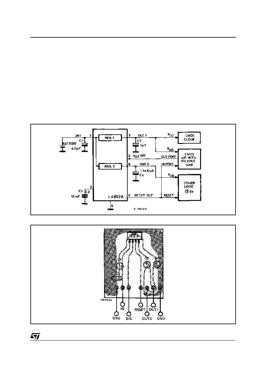
APPLICATION INFORMATION
In power supplies for
µ
P systems it is necessary to
provide power continuously to avoid loss of infor-
mation in memories and in time of day clocks, or to
save datawhen the primary supply is removed.The
L4902A makes it very easy to supply such equip-
ments ; it provides two voltage regulators (both 5V
high precision) with common inputs plus a reset
output for the data save function and a Reg. 2
disable input.
CIRCUIT OPERATION (see Figure 1)
After switch on Reg. 1 saturates until V
01
rises to
the nominal value.
When the input reaches V
IT
and the output 1 is
higher than V
RT
the output 2 (V
02
) switches on and
the reset output (V
R
) also goes high after a pro-
grammable time T
RD
(timing capacitor).
V
02
and V
R
are switched togetherat low level when
one of the following conditions occurs :
- a high level ( V
DT
) is applied on pin 3 ;
- an input overvoltage ;
- an overload on the output 1 (V
01
V
RT
) ;
- a switch off (V
IN
V
IT
- V
ITH
) ;
and they start again as before when the condition
is removed.
An overload on output 2 does not switch Reg. 2,
and does not influence Reg. 1.
The V
01
output features :
- 5V internal reference without voltage divider be-
tween the output and the error comparator
- very low drop series regulator element utilizing
current mirrors
permit high output impedance and then very low
leakage current even in power down condition.
Figure 1
L4902A
4/9
This output may thereforebe usedto supply circuits
continuously, such as volatile RAMs, allowing the
use of a back-up battery.
The V
02
output can supply other non essential 5 V
circuits which may be powered down when the
system is inactive, or that must be powered down
to prevent uncorrect operation for supply voltages
below the minimum value.
The reset output can be usedas a "POWER DOWN
INTERRUPT", permitting RAM access only in cor-
rect power conditions, or as a "BACK-UP ENABLE"
to transfer data into in a NV SHADOW MEMORY
when the supply is interrupted.
The disable function can be used for remote on/off
control of circuits connected to the V
02
output.
APPLICATION SUGGESTIONS
Figure 2 illustrate how the L4902A's disable input
may be used in a CMOS
µ
Computer application.
TheV
01
regulator(low consumption)supply perma-
nently a CMOS time of day clock and a CMOS
µ
computer chip with volatile memory. V
02
output,
supplying non-essential circuits, is turned OFF un-
der control of a
µ
P unit.
Figure 2
Figure 3 : P.C. Board Component Layout of Figure 2
L4902A
5/9

Configurations of this type are used in products
where the OFF switch is part of a keyboard
scanned by a micro which operates continuously
even in the OFF state.
Another application for the L4902A is supplying a
shadow-ram microcomputer chip (SGS M38SH72
for example)where a fast NV memory is backed up
on chip by a EEPROM when a low level on the reset
output occurs.
By adding two CMOS-SCHMIDT-TRIGGER and
few external components, also a watch dog func-
tion may be realized (see Figure 5). During normal
operation the microsystem supplies a periodical
pulse waveform;if an anomalousconditionoccours
(in the program or in the system), the pulses will be
absent and the disable input will be activated after
a settling time determined by R1 C1. In this condi-
tion all the circuitry connected to V
02
will be dis-
abled, the system will be restarted with a new reset
front.
The disable of V
02
prevent spurious operation dur-
ing microprocessor malfunctioning.
Figure 4
Figure 5
L4902A
6/9

Figure 6 :
Quiescent Current versus Output
ICurrent
Figure 7 :
Quiescent Current versus Input Voltage
Figure 8 :
Supply Voltage Rejection
Regulators 1 and 2 versus Input Rip-
ple Frequence
L4902A
7/9

Heptawatt V
DIM.
mm
inch
MIN.
TYP.
MAX.
MIN.
TYP.
MAX.
A
4.8
0.189
C
1.37
0.054
D
2.4
2.8
0.094
0.110
D1
1.2
1.35
0.047
0.053
E
0.35
0.55
0.014
0.022
E1
0.7
0.97
0.028
0.038
F
0.6
0.8
0.024
0.031
F1
0.9
0.035
G
2.34
2.54
2.74
0.095
0.100
0.105
G1
4.88
5.08
5.28
0.193
0.200
0.205
G2
7.42
7.62
7.82
0.295
0.300
0.307
H2
10.4
0.409
H3
10.05
10.4
0.396
0.409
L
16.7
16.9
17.1
0.657
0.668
0.673
L1
14.92
0.587
L2
21.24
21.54
21.84
0.386
0.848
0.860
L3
22.27
22.52
22.77
0.877
0.891
0.896
L4
1.29
0.051
L5
2.6
2.8
3
0.102
0.110
0.118
L6
15.1
15.5
15.8
0.594
0.610
0.622
L7
6
6.35
6.6
0.236
0.250
0.260
L9
0.2
0.008
M
2.55
2.8
3.05
0.100
0.110
0.120
M1
4.83
5.08
5.33
0.190
0.200
0.210
V4
40
∞
(typ.)
Dia
3.65
3.85
0.144
0.152
A
L
L1
C
D1
L5
L2
L3
D
E
M1
M
H3
Dia.
L7
L6
F1
H2
F
G
G1
G2
E1
F
E
L9
V4
L4
H2
V
V
HEPTAMEC
H1
OUTLINE AND
MECHANICAL DATA
L4902A
8/9

Information furnished is believed to be accurate and reliable. However, STMicroelectronics assumes no responsibility for the
consequences of use of such information nor for any infringement of patents or other rights of third parties which may result from
its use. No license is granted by implication or otherwise under any patent or patent right s of STMicroelectronics. Specification
mentioned in this publication are subject to change without notice. This publication supe rsedes and replaces all information
previously supplied. STMicroelectronics products are not authorized for use as criticalcomp onents in life support devices or systems
without express written approval of STMicroelectronics.
The ST logo is a registered trademark of STMicroelectronics
©
2000 STMicroelectronics ≠ Printed in Italy ≠ All Rights Reserved
STMicroelectronics GROUP OF COMPANIES
Australia - Brazil - China - Finland - France - Germany - Hong Kong - India - Italy - Japan - Malaysia - Malta - Morocco -
Singapore - Spain - Sweden - Switzerland - United Kingdom - U.S.A.
http://www.st.com
L4902A
9/9