
L4916
June 2000
VOLTAGE REGULATOR PLUS FILTER
Æ
.
FIXED OUTPUT VOLTAGE 8.5 V
.
250 mA OUTPUT CURRENT
.
HIGH RIPPLE REJECTION
.
HIGH LOAD REGULATION
.
HIGH LINE REGULATION
.
SHORT CIRCUIT PROTECTION
.
THERMAL SHUT DOWN WITH HYSTERESIS
.
DUMP PROTECTION
This circuit combines both a filter and a voltageregu-
lator in order to provide a high ripple rejection over a
wider input voltage range.
A supervisor low-pass loop of the element prevents
the outputtransistor from saturation at low input volt-
ages.
The non linear behaviour of this control circuitry
allows a fast settling of the filter.
POW ER MI NIDIP
(4 + 4)
ORDERING NUMBER : L4916
BLOCK DIAGRAM
DESCRIPTION
1/8

ABSOLUTE MAXIMUM RATINGS
Symbol
Parameter
Value
Unit
V
i
Peak Input Voltage (300 ms)
40
V
V
i
DC Input Voltage
28
V
I
O
Output Current
Internally Limited
P
tot
Power Dissipation
Internally Limited
T
stg
, T
j
Storage and Junction Temperature
≠ 40 to 150
∞
C
PIN CONNECTION (top view)
THERMAL DATA
Symbol
Parameter
Value
Unit
R
th j-amb
R
th j-pins
Thermal Resistance Junction-ambient
Thermal Resistance Junction-pins
Max
Max
80
20
∞
C/W
∞
C/W
L4916
2/8
ELECTRICAL CHARACTERISTICS (T
amb
= 25
∞
C; V
i
= 13.5 V, testcircuit of fig. 1, unlessotherwise specified)
Symbol
Parameter
Test Conditions
Min.
Typ.
Max.
Unit
V
i
Input Voltage
20
V
V
O
Output Voltage
V
i
= 12 to 18 V
I
O
= 5 to 150 mA
8.1
8.5
8.9
V
V
I/O
Controlled
Input-output
Dropout
Voltage
V
i
= 5 to 10 V
I
O
= 5 to 150 mA
1.6
2.1
V
V
O
Line Regulation
V
i
= 12 to 18 V
I
O
= 10 mA
1
20
mV
V
O
Load Regulation
I
O
= 5 to 250 mA
t
on
= 30
µ
s
t
off
=
1 ms
50
100
mV
V
O
Load Regulation
(filter mode)
V
i
= 8.5 V
I
O
= 5 to 150 mA
t
on
= 30
µ
s
t
off
=
1 ms
150
250
mV
I
q
Quiescent Current
I
O
= 5 mA
1
2
mA
I
q
Quiescent Current Change
V
i
= 6 to 18 V
I
O
= 5 to 150 mA
0.05
mA
V
O
T
Output Voltage Drift
I
O
= 10 mA
1.2
mV/
∞
C
SVR
Supply Voltage Rejection
V
iac
= 1 V
rms
f = 100 Hz
I
O
= 150 mA
V
IDC
= 12 to 18 V
V
IDC
= 6 to 11 V
70
35(*)
dB
dB
I
SC
Short Circuit Current
250
300
mA
T
on
Switch On Time
I
O
= 150 mA
V
i
= 5 to 11 V
V
i
= 11 to 18 V
500(*)
300
ms
ms
T
J
Thermal
Shutdown
Junction
Temperature
145
∞
C
( *) D epending of the C
FT
capaci tor.
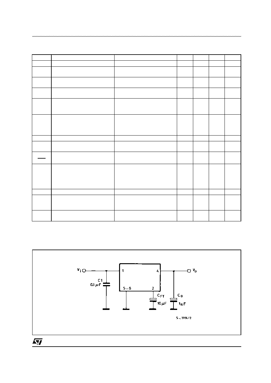
Figure 1 : Test and Application Circuit.
L4916
3/8

Figure 2 : P.C. Board and Component Layout of Fig. 1 (1 : 1 scale).
PRINCIPLE OF OPERATION
During normal operation (input voltage upper than
V
I MIN
= V
OUT NOM
+
V
I/O
). The device works as a
normal voltage regulator built aroundthe OP1 of the
block diagram.
The series pass element use a PNP-NPN connec-
tion to reduce the dropout. The reference voltage of
the OP1 is derived from a REF through the OP2and
Q3, acting as an active zener diode of value V
REF
.
In this condition the device works in the range (1) of
the characteristic of the non linear drop control unit
(see fig.3).
The output voltage is fixed to its nominal value:
R1
V
OUT NOM
= V
REF
(1 +
) =
R2
R1
V
CFT
(1 +
)
R2
R1
= INTERNALLY FIXED RATIO = 2.4
R2
The ripple rejection is quite high (70 dB) and inde-
pendent from C
FT
value.
On the usual voltage regulators, when the input vol-
tage goes below the nominal value, the regulation
transistors (series element) saturate bringing the
system out of regulation making it very sensible to
every variation of the input voltage. On the contrary,
a control loop on the L4916 consents to avoid the
saturation of the series element by regulating the
value of the reference voltage (pin 2). In fact, when-
ever the input voltage decreases below V
I MIN
the
supervisor loop, utilizing a non linear OTA, forces
the reference voltage at pin 2 to decrease by dis-
charging C
FT
. So, during the static mode, when the
input voltage goes below V
MIN
the drop out is kept
fixed to about 1.6V. In this condition the device
works as a low pass filter in the range (2) of the OTA
characteristic. The ripple rejection is externally ad-
justable acting on C
FT
as follows :
V
I
(jw)
SVR (jw) =
=
V
out
(jw)
10
-6
1 +
gm
R1
(1 +
)
jwC
FT
R
2
Where:
gm = 2 . 10
-5
-1
= OTA'S typical transconductance
value on linear region
R1
= fixed ratio
R2
C
FT
= value of capacitor in
µ
F
The reaction time of the supervisor loop is given by
the transconductanceof the OTA and by C
FT
. When
the value of the ripple voltage is so high and its ne-
gative peak is fast enough to determine an istanta-
neous decrease of the dropout till 1.2 V, the OTA
works in a higher transconductance condition
[range (3) of the characteristic] and discharge the
capacitor rapidously.
If the ripple frequency is high enough the capacitor
won't charge itself completely, and the output volt-
age reaches a small value allowinga betterripple re-
jection ; the device's again working as a filter (fast
transient range).
With C
FT
= 10
µ
F; f = 100Hz a SVR of 35 is obtained.
L4916
4/8

Figure 3 : Nonliner Transfer Characteristic of the Drop Control Unit.
Figure 4 : Supply Voltage Rejection vs. Input
Voltage.
Figure 5 : Supply voltage Rejection vs.
Frequency.
Figure 6 : V
o
vs. Supply Voltage.
Figure 7 : Quiescent Current vs. Input Voltage.
1) Normal operating range (high ripple
rejection)
2) Drop controlled range (medium ripple
rejection)
3) Fast discharge of C
FT
L4916
5/8