 | –≠–ª–µ–∫—Ç—Ä–æ–Ω–Ω—ã–π –∫–æ–º–ø–æ–Ω–µ–Ω—Ç: L4922 | –°–∫–∞—á–∞—Ç—å:  PDF PDF  ZIP ZIP |

L4922
June 2000
VERY LOW DROP REGULATOR WITH RESET
Æ
.
VERY LOW DROP (max. 0.9 V at 1 A) OVER
FULL OPERATING TEMPERATURE RANGE
(≠ 40 / + 125
∞
C)
.
LOW QUIESCENT CURRENT (max 70 mA at
1 A) OVER FULL T RANGE
.
PRECISE OUTPUT VOLTAGE (5 V
±
4 %)
OVER FULL T RANGE
.
POWER ON-OFF INFORMATION WITH SET-
TABLE DELAY
.
REVERSE BATTERY PROTECTION
.
SHORT CIRCUIT PROTECTION
.
THERMAL SHUTDOWN
DESCRIPTION
The L4922is a high current monolithic voltage regu-
lator with very low voltage drop (0.70 V max at 1 A,
T
J
= 25
∞
C).
The device is internally protected against load
dumps transient of + 60V, reverse polarity, over-
heating and output short circuit : thanks toted for the
automotive and industrial applications.
Pen tawatt
O RDERING NUMBER : L4922
BLOCK DIAGRAM
1/6
This is advanced information on a new product now in development or undergoing evaluation. Details are subject to change without notice.
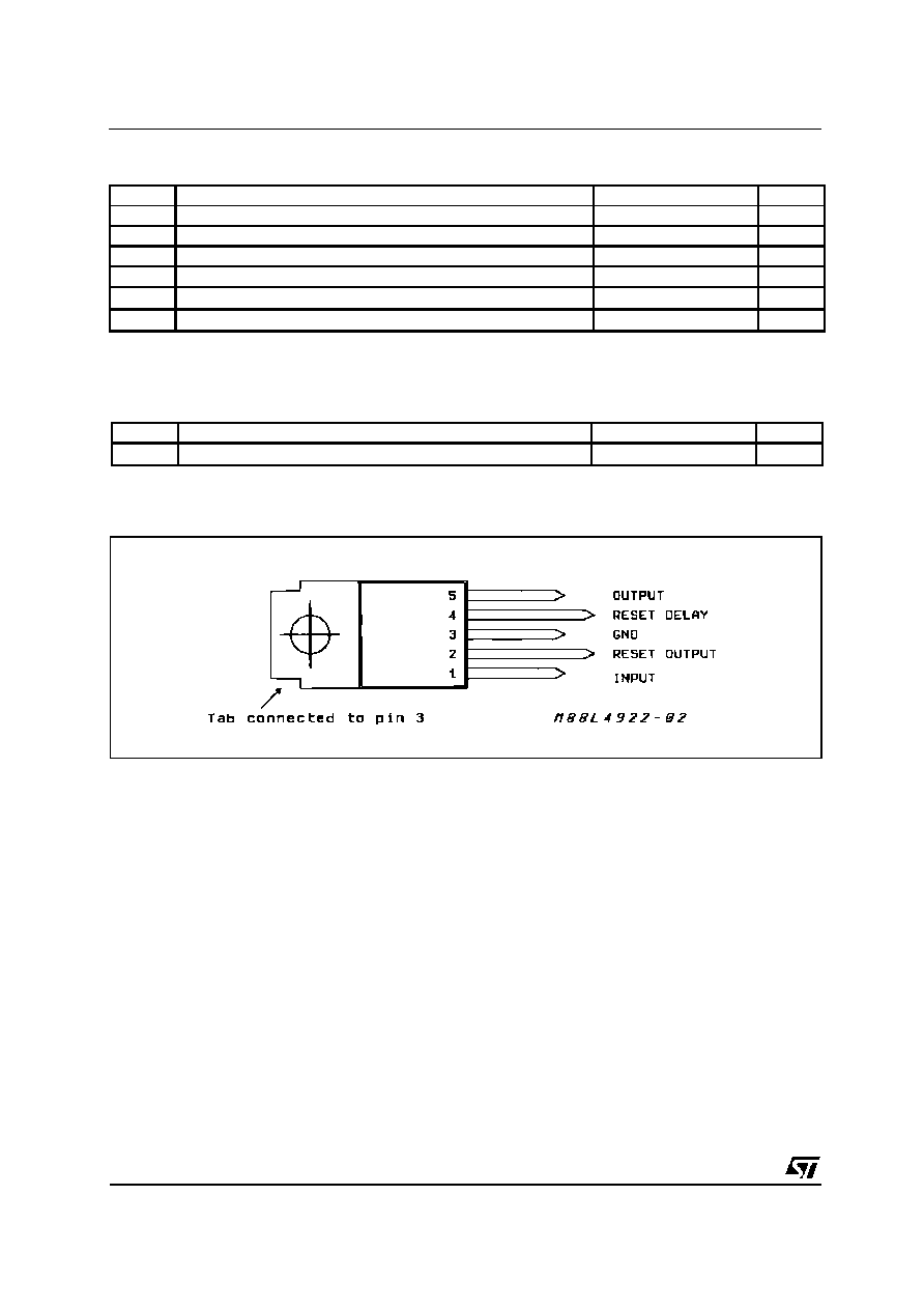
PIN CONNECTION (Top view)
FUNCTIONAL DESCRIPTION
The operating principle of the voltage regulator is
basedon thereference,the error amplifier,the driver
and the power PNP. This stage uses an Isolated
Collector Vertical PNP transistor which allows to ob-
tain very low dropout voltage (typ. 450mV) and low
quiescent current (I
Q
= 20mA typically at I
o
= 1A).
Thanks to these features the device is particularly
suited when the power dissipation must be limited
as, for example, in automotive or industrial applica-
tions supplied by battery.
The three gain stages (operational amplifier,
driver and power PNP) require the external capaci-
tor (Co
min
= 22
µ
F) to guarantee the global stability
of the system.
The antisaturationcircuit allows to reduce drastically
the current peak which takes place during the start
up.
The reset function is LOW active when the output
voltage level is lower than the reset threshold volt-
age V
RthOFF
(typ.value : V
o
≠ 150mV).When the out-
put voltage is higher thanV
RthON
the reset becomes
HIGH aftera delaytime settablewith the externalca-
pacitorC
d
. Typicallyt
d
= 20ms, C
d
= 0.1
µ
F. The reset
and delay threshold hysteresis improve the noise
immunity allowing to avoid false switchings. The
typical reset output waveform is shown in fig. 1.
ABSOLUTE MAXIMUM RATINGS
Symbol
Parameter
Value
Unit
V
i
DC Input Voltage
35
V
V
r
DC Reverse Voltage
≠18
V
V
D
Positive Load Dump Protection (t = 300ms)
60
V
T
J
Junction Temperature Range
≠40 to 150
∞
C
T
op
Operating Temperature Range
≠40 to 125
∞
C
T
stg
Storage Temperature Range
≠55 to 150
∞
C
THERMAL DATA
Symbol
Parameter
Value
Unit
R
th j-case
Thermal Resistance Junction-case
Max.
3.5
∞
C/W
N ote: T he circuit is ESD protected according to MIL-STD -883C
L4922
2/6

ELECTRICAL CHARACTERISTICS (V
i
= 14. 4V, ≠ 40
∞
C
T
J
+ 125
∞
C unless otherwise specified)
Symbol
Parameter
Test Conditions
Min.
Typ.
Max.
Unit
V
i
Operating Input Voltage
(*) Note 1
6
26
V
V
o
Output Voltage
I
o
= 0mA to 1A
T
J
= 25
∞
C
4.8
4.9
5.2
5.1
V
V
V
Line
Line Regulation
V
i
= 6 to 26V;
I
O
= 10mA
5
25
mV
SVR
Supply Voltage Rejection
I
o
= 700mA
f = 120Hz; C
o
= 47
µ
F
V
i
= 12V
dc
+ 5V
pp
55
dB
V
LOAD
Load Regulation
I
o
= 10mA to 1A
15
50
mV
V
i
≠ V
o
Dropout Voltage
T
J
= 25
∞
C, I
O
= 1A
0.45
0.70
V
Over Full T, I
o
= 1A
0.90
V
I
q
Quiescent Current
I
o
= 10mA
I
o
= 1A
7
25
12
70
mA
mA
I
SC
Short Circuit Current
1.8
A
V
R
Rset Output Saturation Voltage
1.5V < V
O
< V
RT (off)
, I
R
= 1.6mA
3V < V
O
< V
RT (off)
, I
R
= 8mA
0.40
0.40
V
V
V
RT peak
Power On-Off Reset out Peak
Voltage
1K
Reset Pull-up to V
O
0.65
1.0
V
I
R
Reset Output Leakage Current
(high level)
V
o
in Regul.
V
R
= 5V
50
µ
A
t
D
Reset Pulse Delay Time
C
D
= 100nF
20
ms
V
RthOFF
Power OFF V
o
Threshold
V
o
@ Reset out H to L
Transition; T
J
= 25
∞
C
≠ 40
∞
C
T
J
+ 125
∞
C
4.75
4.70
V
o
≠0.15
V
V
I
C6
Delay Capacitor Charging
Current (current generator)
V
4
= 3V
20
µ
A
V
RthON
Power ON V
o
Threshold
V
o
@ Reset out L to H
Transition
V
rthOFF
+ 0.03V
V
o
≠
0.04V
V
V
4
Delay Comparator Threshold
Reset out = "1" H to L Transition
3.2
3.8
V
Reset out = "0" L to H Transition
3.7
4
4.4
V
V
6H
Delay Comparator Hysteresis
500
mV
(*) Note 1 : The device is not operating within the range : 26 V < V
i
< 37 V.
EXTERNAL COMPENSATION
Since the purpose of a voltageregulatoris to supply
a fixed output voltage in spite of supply and load
variations, the open loop gain of the regulator must
be very high at low frequencies.This may cause in-
stability as a result of the various poles present in
the loop. To avoid this instability dominant pole
compensationis used to reduce phase shiftsdue to
other poles at the unity gain frequency. The lower
the frequencyof theseother poles, the greater must
be the capacitor used to create the dominant pole
for the same DC gain.
Where the output transistor is a lateral PNP type
there is a pole in the regulation loop at a frequency
too low to be compensated by a capacitor wich can
be integrated. An external compensation is there-
fore necessary so a very high value capacitor must
be connected from the output to ground.
The parassitic equivalentseries resistanceof theca-
pacitor used adds a zero to the regulation loop. This
zero may compromise the stability of the system
since its effect tends to cancel the effect of the pole
added. In regulators this ESR must be less than 3
and the minimum capacitor value is 47
µ
F.
L4922
3/6
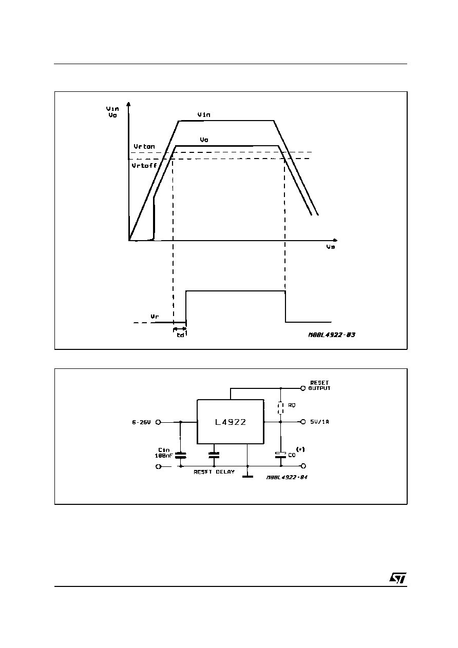
Figure 1 : Typical Reset Output Waveform.
Figure 2 : Typical Application Circuit.
(*) RECOMMENDED VALUE : C
0
= 47
µ
F, ESR < 10 ohm, (I
out
> 10 mA) OVER FULL T
range
.
L4922
4/6
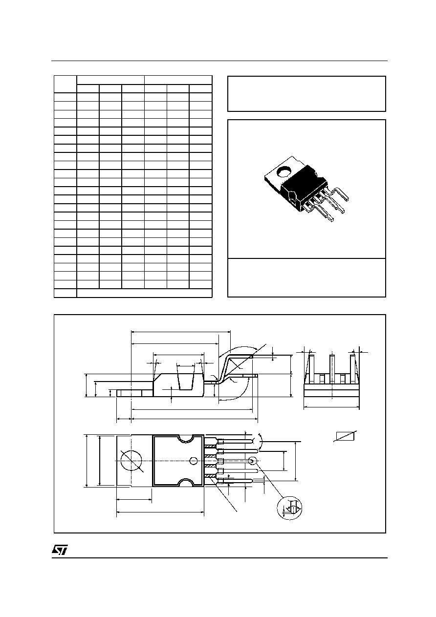
Pentawatt V
DIM.
mm
inch
MIN.
TYP.
MAX.
MIN.
TYP.
MAX.
A
4.8
0.189
C
1.37
0.054
D
2.4
2.8
0.094
0.110
D1
1.2
1.35
0.047
0.053
E
0.35
0.55
0.014
0.022
E1
0.76
1.19
0.030
0.047
F
0.8
1.05
0.031
0.041
F1
1
1.4
0.039
0.055
G
3.2
3.4
3.6
0.126
0.134
0.142
G1
6.6
6.8
7
0.260
0.268
0.276
H2
10.4
0.409
H3
10.05
10.4
0.396
0.409
L
17.55
17.85
18.15
0.691
0.703
0.715
L1
15.55
15.75
15.95
0.612
0.620
0.628
L2
21.2
21.4
21.6
0.831
0.843
0.850
L3
22.3
22.5
22.7
0.878
0.886
0.894
L4
1.29
0.051
L5
2.6
3
0.102
0.118
L6
15.1
15.8
0.594
0.622
L7
6
6.6
0.236
0.260
L9
0.2
0.008
M
4.23
4.5
4.75
0.167
0.177
0.187
M1
3.75
4
4.25
0.148
0.157
0.167
V4
40
∞
(typ.)
L
L1
A
C
L5
D1
L2
L3
E
M1
M
D
H3
Dia.
L7
L6
F1
H2
F
G G1
E1
F
E
L9
V4
R
R
R
RESIN BETWEEN
LEADS
H1
V3
H2
L8
V
V
V1
B
V
V
V4
V4
OUTLINE AND
MECHANICAL DATA
L4922
5/6