 | –≠–ª–µ–∫—Ç—Ä–æ–Ω–Ω—ã–π –∫–æ–º–ø–æ–Ω–µ–Ω—Ç: L4923 | –°–∫–∞—á–∞—Ç—å:  PDF PDF  ZIP ZIP |

L4923
June 2000
WITH RESET AND INHIBIT
5V≠1A VERY LOW DROP REGULATOR
Æ
.
VERY LOW DROP (max. 0.9V at 1A) OVER
FULL OPERATING TEMPERATURE RANGE
(≠ 40 / + 125
∞
C)
.
LOW QUIESCENT CURRENT (max 70 mA at
1 A) OVER FULL T RANGE
.
PRECISEOUTPUT VOLTAGE(5V
±
4%) OVER
FULL T RANGE
.
POWER ON-OFF INFORMATION WITH SET-
TABLE DELAY
.
INHIBIT FOR REMOTE ON-OFF COMMAND
(active high)
.
LOAD STANDBY CURRENT
.
LOAD DUMP AND REVERSE BATTERY PRO-
TECTION
.
SHORT CIRCUIT PROTECTION
.
THERMAL SHUTDOWN
DESCRIPTION
The L4923is a high current monolithic voltage regu-
lator with very low voltage drop (0.70 V max at 1 A,
T
J
= 25
∞
C).
The device is internally protected against load
dumps transient of + 60 V, input overvoltage, re-
verse polarity, overheating and output short circuit :
thanks to these featuresthe L4923is very suited for
the automotive and industrial applications.
The reset function is very useful for power off and
power on information when supplying a microproc-
essor.
The inhibit function reduces drastically the con-
sumption when no load current is required : typically
the standby current value is 300
µ
A.
Heptawatt
ORDERING NUMBER : L4923
BLOCK DIAGRAM
1/6
This is advanced information on a new product now in development or undergoing evaluatio n. Details are subject to change without notice.

PIN CONNECTION
ABSOLUTE MAXIMUM RATINGS
Symbol
Parameter
Value
Unit
V
i
DC Input Voltage
35
V
V
r
DC Reverse Voltage
≠ 18
V
V
D
Positive Load Dump Protection (t = 300ms)
60
V
T
J
Junction Temperature range
≠ 40 to 150
∞
C
T
op
Operating Temperature Range
≠ 40 to 125
∞
C
T
stg
Storage Temperature Range
≠ 55 to 150
∞
C
THERMAL DATA
Symbol
Parameter
Value
Unit
R
th j-case
Thermal Resistance Junction Case
4
∞
C/W
Figure 1 : Application Circuit.
(*) RECOMMENDED VALUE : C
0
= 47
µ
F, ESR < 10
, (I
out
> 10 mA) OVER FULL T
range
.
Note: The circuit is ESD protected according to MIL-STD-883C
L4923
2/6

ELECTRICAL CHARACTERISTICS (V
i
= 14. 4V, ≠ 40
∞
C
T
J
+ 125
∞
C unless otherwise specified)
Symbol
Parameter
Test Conditions
Min.
Typ.
Max.
Unit
V
i
Operating Input Voltage
(*) Note 1
6
26
V
V
o
Output Voltage
I
o
= 0mA to 1A
T
J
= 25
∞
C
4.8
4.9
5.2
5.1
V
V
V
Line
Line Regulation
V
i
= 6 to 26V;
I
O
= 10mA
5
25
mV
SVR
Supply Voltage Rejection
I
o
= 700mA
f = 120Hz; C
o
= 47
µ
F
V
i
= 12V
dc
+ 5V
pp
55
dB
V
LOAD
Load Regulation
I
o
= 10mA to 1A
15
50
mV
V
i
≠ V
o
Dropout Voltage
T
J
= 25
∞
C, I
O
= 1A
0.45
0.70
V
Over Full T, I
o
= 1A
0.90
V
I
q
Quiescent Current
I
o
= 10mA
I
o
= 1A
Active High Inhibit
7
25
0.30
12
70
0.65
mA
mA
mA
I
SC
Short Circuit Current
1.8
A
SVR
Supply Volt. Rej.
I
o
= 350mA ; f = 120Hz
C
o
= 100
µ
F ; V
i
= 12V
±
5V
pp
50
60
dB
V
R
Rset Output Saturation Voltage
1.5V < V
O
< V
RT (off)
, I
R
= 1.6mA
3V < V
O
< V
RT (off)
, I
R
= 8mA
0.40
0.40
V
V
V
RT peak
Power On-Off Reset out Peak
Voltage
1K
Reset Pull-up to V
O
0.65
1.0
V
I
R
Reset Output Leakage Current
(high level)
V
o
in Regul.
V
R
= 5V
50
µ
A
t
D
Reset Pulse Delay Time
C
D
= 100nF
20
ms
V
RthOFF
Power OFF V
o
Threshold
V
o
@ Reset out H to L
Transition; T
J
= 25
∞
C
≠ 40
∞
C
T
J
+ 125
∞
C
4.75
4.7
V
o
≠ 0.15
V
V
I
C6
Delay Capacitor Charging
Current (current generator)
V
6
= 3V
20
µ
A
V
RthON
Power ON V
o
Threshold
V
o
@ Reset out L to H
Transition
V
rthOFF
+ 0.03V
V
o
≠
0.04V
V
V
6
Delay Comparator Threshold
Reset out = "1" H to L Transition
3.2
3.8
V
Reset out = "0" L to H Transition
3.7
4
4.4
V
V
6H
Delay Comparator Hysteresis
500
mV
V
InhL
Low Inhibit Voltage
0.5
V
V
InhH
High Inhibit Voltage
2.0
V
I
InhL
Low Level Inhibit Current
V
Inh L
= 0.4V
≠ 40
≠ 10
µ
A
(*) Note 1 : The device is not operating within the range : 26 V < V
i
< 37 V.
EXTERNAL COMPENSATION
Since the purpose of a voltageregulatoris to supply
a fixed output voltage in spite of supply and load
variations, the open loop gain of the regulator must
be very high at low frequencies.This may cause in-
stability as a result of the various poles present in
the loop. To avoid this instability dominant pole
compensationis used to reduce phase shifts due to
other poles at the unity gain frequency. The lower
the frequency of theseother poles, the greatermust
be the capacitor used to create the dominant pole
for the same DC gain.
Where the output transistor is a lateral PNP type
there is a pole in the regulation loop at a frequency
too low to be compensatedby a capacitor wich can
be integrated. An external compensation is there-
fore necessary so a very high value capacitor must
be connectedfrom the output to ground.
The parassiticequivalentseries resistance of theca-
pacitor used adds a zero to the regulationloop. This
zero may compromise the stability of the system
since its effect tends to cancel the effect of the pole
added. In regulators this ESR must be less than 3
and the minimum capacitor value is 47
µ
F.
L4923
3/6

The operating principle of the voltage regulator is
basedon thereference,the error amplifier,the driver
and the power PNP. This stage uses an Isolated
Collector Vertical PNP transistor which allows to ob-
tain very low dropout voltage (typ. 450 mV) and low
quiescent current (I
Q
= 20 mA typically at I
O
= 1 A).
Thanks to these features the device is particularly
suited when the power dissipation must be limited
as, for example, in automotive or industrial applica-
tions supplied by battery.
The three gain stages (operational amplifier, driver
and power PNP) require the external capacitor
(C
Omin
= 22
µ
F) to guarantee the global stability of
the system.
The antisaturationcircuit allows to reducedrastically
the current peak which takes place during the start
up.
The reset function is LOW active when the output
voltage level is lower than the reset threshold volt-
age V
Rth
(typ.value : V
O
- 150 mV). When the output
voltage is higher than V
Rth
the reset becomes HIGH
after a delay time settablewith the externalcapacitor
C
d
. Typically t
d
= 20 ms, C
d
= 0.1
µ
F. The reset
threshold hysteresis improves the noise immunity
allowing to avoid false switchings. The typical reset
output waveform is shown in fig. 2.
The inhibit circuit acceptsstandardTTL inputlevels :
thisblockswitches off the voltage regulatorwhen the
input signal is HIGH and switches on it when the in-
put signal is LOW. Thanksto inhibit functionthe con-
sumption is drastically reduced (650
µ
A max) when
no load current is required.
Figure 2 : Typical Reset Output Waveform.
FUNCTIONAL DESCRIPTION
L4923
4/6
Heptawatt V
DIM.
mm
inch
MIN.
TYP.
MAX.
MIN.
TYP.
MAX.
A
4.8
0.189
C
1.37
0.054
D
2.4
2.8
0.094
0.110
D1
1.2
1.35
0.047
0.053
E
0.35
0.55
0.014
0.022
E1
0.7
0.97
0.028
0.038
F
0.6
0.8
0.024
0.031
F1
0.9
0.035
G
2.34
2.54
2.74
0.095
0.100
0.105
G1
4.88
5.08
5.28
0.193
0.200
0.205
G2
7.42
7.62
7.82
0.295
0.300
0.307
H2
10.4
0.409
H3
10.05
10.4
0.396
0.409
L
16.7
16.9
17.1
0.657
0.668
0.673
L1
14.92
0.587
L2
21.24
21.54
21.84
0.386
0.848
0.860
L3
22.27
22.52
22.77
0.877
0.891
0.896
L4
1.29
0.051
L5
2.6
2.8
3
0.102
0.110
0.118
L6
15.1
15.5
15.8
0.594
0.610
0.622
L7
6
6.35
6.6
0.236
0.250
0.260
L9
0.2
0.008
M
2.55
2.8
3.05
0.100
0.110
0.120
M1
4.83
5.08
5.33
0.190
0.200
0.210
V4
40
∞
(typ.)
Dia
3.65
3.85
0.144
0.152
A
L
L1
C
D1
L5
L2
L3
D
E
M1
M
H3
Dia.
L7
L6
F1
H2
F
G
G1
G2
E1
F
E
L9
V4
L4
H2
V
V
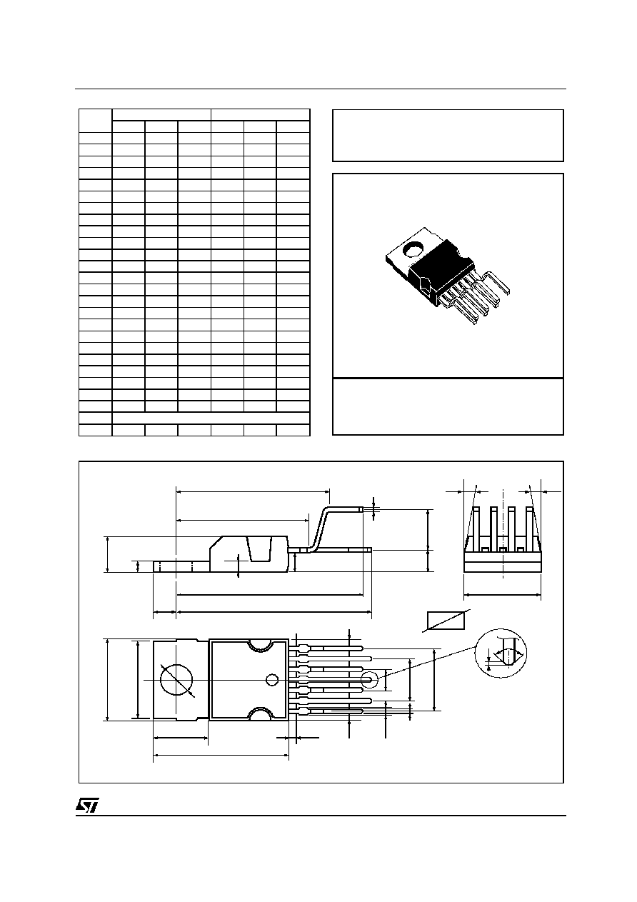
HEPTAMEC
H1
OUTLINE AND
MECHANICAL DATA
L4923
5/6

Information furnished is believed to be accurate and reliable. However, STMicroelectronics assumes no responsibility for the conse-
quences of use of such information nor for any infringement of patents or other rights of third parties which may result from its use. No
license is granted by implication or otherwise under any patent or patent rights of STMicroelectronics. Specification mentioned in this
publication are subject to change without notice. This publication supersedes and replaces all information previously supplied. STMi-
croelectronics products are not authorized for use as critical components in life support devices or systems without express written
approval of STMicroelectronics.
The ST logo is a registered trademark of STMicroelectronics
©
2000 STMicroelectronics ≠ Printed in Italy ≠ All Rights Reserved
STMicroelectronics GROUP OF COMPANIES
Australia - Brazil - China - Finland - France - Germany - Hong Kong - India - Italy - Japan - Malaysia - Malta - Morocco -
Singapore - Spain - Sweden - Switzerland - United Kingdom - U.S.A.
http://www.st.com
L4923
6/6