 | –≠–ª–µ–∫—Ç—Ä–æ–Ω–Ω—ã–π –∫–æ–º–ø–æ–Ω–µ–Ω—Ç: L4941B | –°–∫–∞—á–∞—Ç—å:  PDF PDF  ZIP ZIP |

1/14
February 2003
s
LOW DROPOUT VOLTAGE (450mV Typ. at
1A)
s
VERY LOW QUIESCENT CURRENT
s
THERMAL SHUTDOWN
s
SHORT CIRCUIT PROTECTION
s
REVERSE POLARITY PROTECTION
DESCRIPTION
The L4941 is a three terminal 5V positive
regulators available in TO-220, TO-220FP and
D
2
PAK packages, making it useful in a wide range
of industrial and consumer applications. Thanks to
its very low input/output voltage drop, these
devices
are
particularly
suitable
for
battery
powered equipments, reducing consumption and
prolonging battery life. It employs internal current
limiting, antisaturation circuit, thermal shut-down
and safe area protection.
L4941
VERY LOW DROP 1A REGULATOR
BLOCK DIAGRAM
TO-220
D
2
PAK
TO-220FP
DPAK

L4941
2/14
ABSOLUTE MAXIMUM RATINGS
Absolute Maximum Ratings are those values beyond which damage to the device may occur. Functional operation under these condition is
not implied.
THERMAL DATA
CONNECTION DIAGRAM (top view)
ORDERING CODES
(*) Available in Tape & Reel with the suffix "-TR".
Symbol
Parameter≤
Value
Unit
V
I
Forward Input Voltage
30
V
V
IR
Reverse Input Voltage (R
O
=100
)
-15
V
I
O
Output Current
Internally Limited
mA
P
D
Power Dissipation
Internally Limited
mW
T
stg
Storage Temperature Range
-40 to +150
∞C
T
op
Operating Junction Temperature Range
-40 to +150
∞C
Symbol
Parameter
TO-220
TO-220FP
D
2
PAK
DPAK
Unit
R
thj-case
Thermal Resistance Junction-case
3
5
3
8
∞C/W
R
thj-amb
Thermal Resistance Junction-ambient
50
60
62.5
100
∞C/W
TO-220
TO-220FP
D
2
PAK
DPAK
ORDERING CODE
PACKAGE
L4941BV
TO-220
L4941BP
TO-220FP
L4941BD2T
D
2
PAK
L4941BDT (*)
DPAK

L4941
3/14
TEST CIRCUITS
Figure 1 : DC Parameter
Figure 2 : Load Rejection
Figure 3 : Ripple Rejection

L4941
4/14
ELECTRICAL CHARACTERISTICS (Refer to test circuit, V
I
=7V, C
I
= 0.1
µ
F, C
O
= 22
µ
F,
T
J
= 25∞C, unless otherwise specified.)
TYPICAL CHARACTERISTICS
Figure 4 : Dropout Voltage vs Output Current
Figure 5 : Dropout Voltage vs Temperature
Symbol
Parameter
Test Conditions
Min.
Typ.
Max.
Unit
V
O
Output Voltage
I
O
= 5mA to 1A
V
I
= 6 to 14V
4.8
5
5.2
V
V
I
Input Voltage
I
O
= 5 mA
16
V
V
O
Line Regulation
V
I
= 6 to 16V
I
O
= 5 mA
5
20
mV
V
O
Load Regulation
I
O
= 5mA to 1A
8
20
mV
I
O
= 0.5A to 1A
5
15
mV
I
q
Quiescent Current
I
O
= 5 mA
V
I
= 6V
4
8
mA
I
O
= 1A
V
I
= 6V
20
40
mA
I
q
Quiescent Current Change
I
O
= 5 mA
V
I
= 6 to 14V
3
mA
I
O
= 1A
V
I
= 6 to 14V
-10
mA
V
d
Dropout Voltage
I
O
= 0.5A
250
450
mV
I
O
= 1A
450
700
mV
V
O
/
T Output Voltage Drift
0.6
mv/∞C
SVR
Supply Voltage Rejection
f = 120Hz
I
O
= 1A
58
68
dB
I
sc
Short Circuit Current
V
I
= 14V
1.6
2.0
A
V
I
= 6V
1.8
2.2
Z
O
Output Impedance
f = 1KHz
I
O
= 0.5A
30
m
e
N
Output Noise Voltage
B = 100Hz to 100KHz
30
µ
V/V
O

L4941
5/14
Figure 6 : Output Voltage vs Temperature
Figure 7 : Quiescent Current vs Temperature
Figure 8 : Quiescent Current vs Input Voltage
Figure 9 : Quiescent Current vs Output Current
Figure 10 : Short Circuit Current vs Temperature
Figure 11 : Peak Output Current vs Input/Output
Differential Voltage

L4941
6/14
Figure 12 : Low Voltage Behavior
Figure 13 : Supply Voltage Rejection vs
Frequency
Figure 14 : Supply Voltage Rejection vs Output
Current
Figure 15 : Load Dump Characteristics
Figure 16 : Line Transient Response
Figure 17 : Total Power Dissipation

L4941
7/14
Figure 18 : Load transient Response
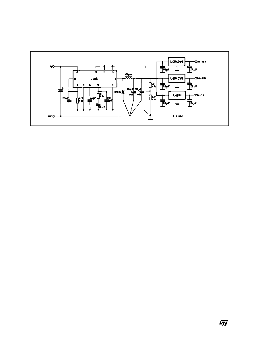
Figure 19 : Distributed Supply with On-card L4940 and L4941 low drop regulator
L4941
8/14
Figure 20 : Distributed Supply with On-card L4940 and L4941 low drop regulator
ADVANTAGES OTF THESE APPLICATION ARE:
On card regulation with short-circuit and thermal protection on each output.
Vary high total system efficency due to the switching preregulation and very low-drop postregulation
L4941
9/14
DIM.
mm.
inch
MIN.
TYP
MAX.
MIN.
TYP.
MAX.
A
4.40
4.60
0.173
0.181
C
1.23
1.32
0.048
0.051
D
2.40
2.72
0.094
0.107
D1
1.27
0.050
E
0.49
0.70
0.019
0.027
F
0.61
0.88
0.024
0.034
F1
1.14
1.70
0.044
0.067
F2
1.14
1.70
0.044
0.067
G
4.95
5.15
0.194
0.203
G1
2.4
2.7
0.094
0.106
H2
10.0
10.40
0.393
0.409
L2
16.4
0.645
L4
13.0
14.0
0.511
0.551
L5
2.65
2.95
0.104
0.116
L6
15.25
15.75
0.600
0.620
L7
6.2
6.6
0.244
0.260
L9
3.5
3.93
0.137
0.154
DIA.
3.75
3.85
0.147
0.151
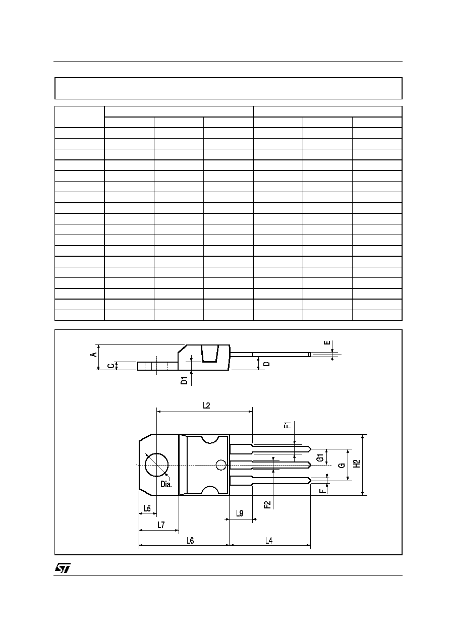
TO-220 MECHANICAL DATA
P011C

L4941
10/14
DIM.
mm.
inch
MIN.
TYP
MAX.
MIN.
TYP.
MAX.
A
4.40
4.60
0.173
0.181
B
2.5
2.7
0.098
0.106
D
2.5
2.75
0.098
0.108
E
0.45
0.70
0.017
0.027
F
0.75
1
0.030
0.039
F1
1.15
1.50
0.045
0.059
F2
1.15
1.50
0.045
0.059
G
4.95
5.2
0.194
0.204
G1
2.4
2.7
0.094
0.106
H
10.0
10.40
0.393
0.409
L2
16
0.630
L3
28.6
30.6
1.126
1.204
L4
9.8
10.6
0.385
0.417
L6
15.9
16.4
0.626
0.645
L7
9
9.3
0.354
0.366
DIA.
3
3.2
0.118
0.126
TO-220FP MECHANICAL DATA
L2
A
B
D
E
H
G
L6
Ø
F
L3
G1
1 2 3
F2
F1
L7
L4
7012510/F

L4941
11/14
DIM.
mm.
inch
MIN.
TYP
MAX.
MIN.
TYP.
MAX.
A
4.4
4.6
0.173
0.181
A1
2.49
2.69
0.098
0.106
A2
0.03
0.23
0.001
0.009
B
0.7
0.93
0.027
0.036
B2
1.14
1.7
0.044
0.067
C
0.45
0.6
0.017
0.023
C2
1.23
1.36
0.048
0.053
D
8.95
9.35
0.352
0.368
D1
8
0.315
E
10
10.4
0.393
0.409
E1
8.5
0.335
G
4.88
5.28
0.192
0.208
L
15
15.85
0.590
0.624
L2
1.27
1.4
0.050
0.055
L3
1.4
1.75
0.055
0.068
M
2.4
3.2
0.094
0.126
R
0.4
0.016
V2
0∞
8∞
0∞
8∞
D
2
PAK MECHANICAL DATA
P011P6G

L4941
12/14
DIM.
mm.
inch
MIN.
TYP
MAX.
MIN.
TYP.
MAX.
A
2.2
2.4
0.086
0.094
A1
0.9
1.1
0.035
0.043
A2
0.03
0.23
0.001
0.009
B
0.64
0.9
0.025
0.035
B2
5.2
5.4
0.204
0.212
C
0.45
0.6
0.017
0.023
C2
0.48
0.6
0.019
0.023
D
6
6.2
0.236
0.244
E
6.4
6.6
0.252
0.260
G
4.4
4.6
0.173
0.181
H
9.35
10.1
0.368
0.397
L2
0.8
0.031
L4
0.6
1
0.023
0.039
DPAK MECHANICAL DATA
0068772-B

L4941
13/14
DIM.
mm.
inch
MIN.
TYP
MAX.
MIN.
TYP.
MAX.
A
180
7.086
C
12.8
13.0
13.2
0.504
0.512
0.519
D
20.2
0.795
N
60
2.362
T
14.4
0.567
Ao
6.80
6.90
7.00
0.268
0.272
0.2.76
Bo
10.40
10.50
10.60
0.409
0.413
0.417
Ko
2.55
2.65
2.75
0.100
0.104
0.105
Po
3.9
4.0
4.1
0.153
0.157
0.161
P
7.9
8.0
8.1
0.311
0.315
0.319
Tape & Reel DPAK-PPAK MECHANICAL DATA

L4941
14/14
Information furnished is believed to be accurate and reliable. However, STMicroelectronics assumes no responsibility for the
consequences of use of such information nor for any infringement of patents or other rights of third parties which may result from
its use. No license is granted by implication or otherwise under any patent or patent rights of STMicroelectronics. Specifications
mentioned in this publication are subject to change without notice. This publication supersedes and replaces all information
previously supplied. STMicroelectronics products are not authorized for use as critical components in life support devices or
systems without express written approval of STMicroelectronics.
© The ST logo is a registered trademark of STMicroelectronics
© 2003 STMicroelectronics - Printed in Italy - All Rights Reserved
STMicroelectronics GROUP OF COMPANIES
Australia - Brazil - Canada - China - Finland - France - Germany - Hong Kong - India - Israel - Italy - Japan - Malaysia - Malta - Morocco
Singapore - Spain - Sweden - Switzerland - United Kingdom - United States.
© http://www.st.com