 | –≠–ª–µ–∫—Ç—Ä–æ–Ω–Ω—ã–π –∫–æ–º–ø–æ–Ω–µ–Ω—Ç: L4947PD | –°–∫–∞—á–∞—Ç—å:  PDF PDF  ZIP ZIP |
L4947PD
5V-0.5A VERY LOW DROP REGULATOR WITH RESET
PRECISE OUTPUT VOLTAGE (5V
±
4%)
OVER FULL TEMPERATURE RANGE
(≠ 40 / 125
∞
C)
VERY LOW VOLTAGE DROP (0.75Vmax)
OVER FULL T RANGE
OUTPUT CURRENT UP TO 500mA
RESET FUNCTION
POWER-ON RESET DELAY PULSE DE-
FINED BY THE EXTERNAL CAPACITOR
+ 80V LOAD DUMP PROTECTION
≠ 80V LOAD DUMP PROTECTION
REVERSE VOLTAGE PROTECTION
SHORT CIRCUIT PROTECTION AND THER-
MAL SHUT-DOWN (with hysteresis)
LOW START UP CURRENT
DESCRIPTION
The L4947PD is a monolithic integrated circuit in
HiPSO package specially designed to provide a
stabilized supply voltage for automotive and in-
dustrial electronic systems. Thanks to its very low
voltage drop, in automotive applications the
L4947PD can work correctly even during the
cranking phase, when the battery voltage could
fall as low as 6V. Furthermore, it incorporates a
complete range of protection circuits against the
dangerous overvoltages always present on the
battery rail of the car. The reset function makes
the device particularly suited to supply microproc-
essor based systems : a signal is available (after
an externally programmable delay) to reset the
microprocessor at power-on phase ; at power-off,
this signal becomes low inhibiting the microproc-
essor.
This is advanced information on a new product now in development or undergoing evaluation. Details are subject to change without notice.
June 2000
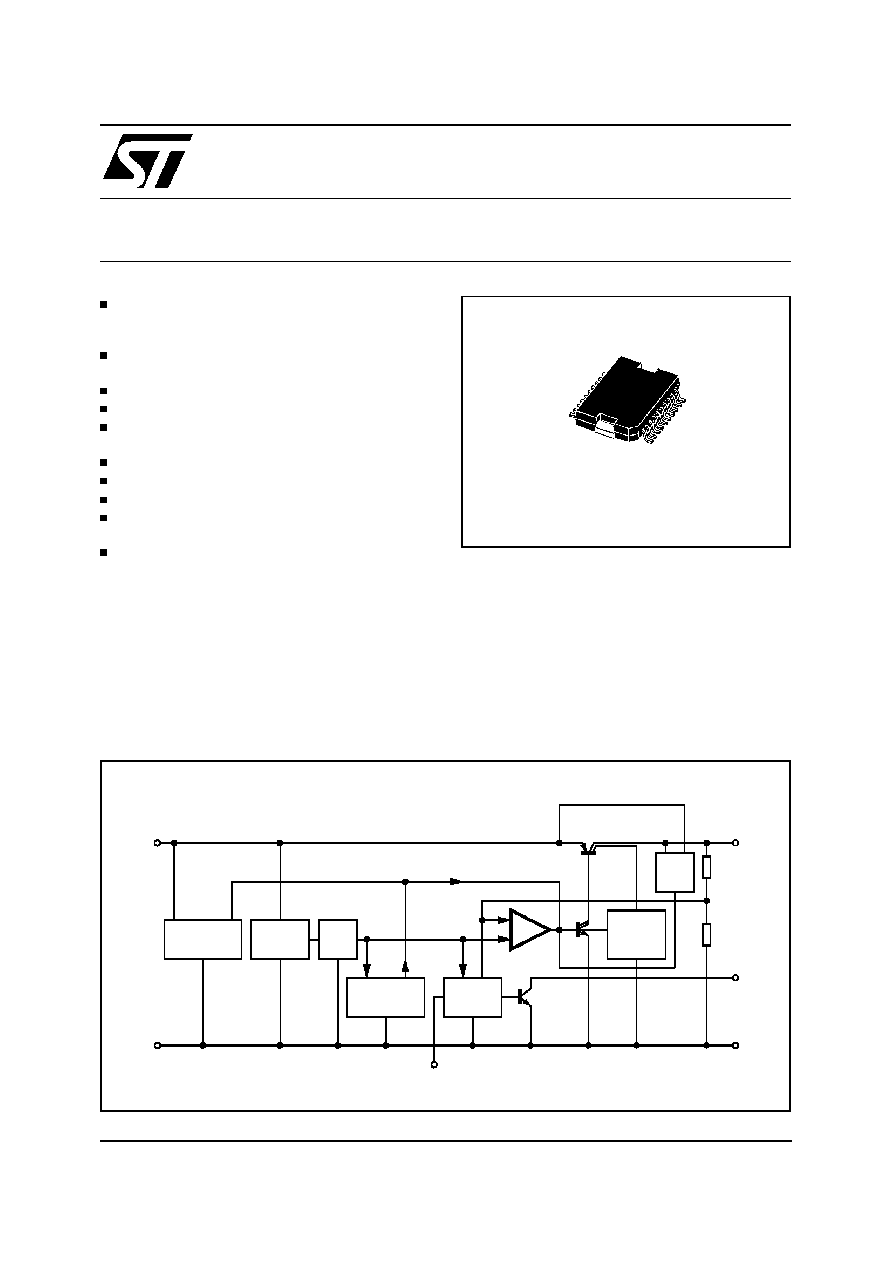
Æ
DUMP
PROTECT.
START
REF.
THERMAL
PROTECTION
RESET
CIRCUIT
ERROR
AMP.
OUTPUT
CURRENT
LIMITER
ANTI
SAT.
PNP OUTPUT
TRANSISTOR
D94AT106
17
1-20
INPUT
DELAY CAPACITOR
2
OUTPUT
3
RESET
OUTPUT
19
GROUND
1-20
BLOCK DIAGRAM
PowerSO20
ORDERING NUMBER: L4947PD
1/6

ABSOLUTE MAXIMUM RATINGS
Symbol
Parameter
Value
Unit
V
i
DC Input Voltage
DC Reverse Input Voltage
Transient Input Overvoltages :
Load Dump :
5ms
t
rise
10ms
f
Fall Time Constant = 100ms
R
SOURCE
0.5
Field Decay :
5ms
t
fall
10ms, R
SOURCE
10
r
Rise Time Constant = 33ms
Low Energy Spike :
t
rise
= 1
µ
s, t
fall
= 500
µ
s, R
SOURCE
10
f
r
Repetition Frequency = 5Hz
35
≠ 18
80
≠ 80
±
100
V
V
V
V
V
V
R
Reset Output Voltage
35
V
T
J
, T
stg
Junction and Storage Temperature Range
≠ 55 to 150
∞
C
Note: The circuit is ESD protected according to MIL-STD-883C.
THERMAL DATA
Symbol
Parameter
Value
Unit
R
th j-case
Thermal Resistance Junction-case
Max
3
∞
C/W
GND
DELAY CAP.
+V
OUT
N.C.
N.C.
N.C.
N.C.
N.C.
N.C.
1
3
2
4
5
6
7
8
9
N.C.
N.C.
N.C.
N.C.
N.C.
+V
IN
N.C.
RESET
GND
20
19
18
17
16
14
15
13
12
D94AT107A
GND
10
GND
11
PIN CONNECTION (Top view)
L4947PD
IN
Ci
100nF
100nF
Cd
17
2
1-20
19
3
OUT
RESET
OUTPUT
Co
47
µ
F(*)
R
P
D94AT108
(*) Min 20
µ
F, ESR <10
over full temperature range
R
P
(pull up resistor) and R
L
(load) are both equal to 1k
.
TEST CIRCUIT
L4947PD
2/6
FUNCTIONAL DESCRIPTION
The L4947PD is a very low drop 5V/0.5A voltage
regulator provided with a reset function and there-
fore particularly suited to meet the requirements
of supplying the microprocessor systems used in
automotive and industrial applications.
The block diagram shows the basic structure of
the device : the reference, the error amplifier, the
driver, the power PNP, the protection and reset
functions.
The power stage is a Lateral PNP transistor
which allows a very low dropout voltage (typ.
400mV at T
J
= 25
∞
C, max. 750mV over the full
temperature range @ I
O
= 500mA). The typical
curve of the dropout voltage as a function of the
junction temperature is shown in Fig. 1 : that is
the worst case, where I
O
= 500mA.
The current consumption of the device (quiescent
ELECTRICAL CHARACTERISTICS (refer to the test circuit, V
i
= 14. 4V, C
o
= 47
µ
F, ESR < 10
,
R
p
= 1K
, R
L
= 1K
, ≠40
∞
C
T
J
125
∞
C, unless otherwise specified)
Symbol
Parameter
Test Conditions
Min.
Typ.
Max.
Unit
V
o
Output Voltage
I
o
= 0mA to 500mA
Over Full T Range
T
J
= 25
∞
C
4.80
4.90
5.00
5.00
5.20
5.10
V
V
V
i
Operating Input Voltage
I
o
= 0mA to (*) 500mA
6
26
V
V
o
Line Regulation
V
i
= 6V to 26V ;
I
o
= 5mA
5
50
mV
V
o
Load Regulation
I
o
= 5mA to 500mA
15
60
mV
V
i
≠V
o
Dropout Voltage
I
o
= 500mA, T
J
= 25
∞
C
Over Full T Range
0.40
0.55
0.75
V
V
I
q
Quiescent Current
I
o
= 0mA, T
J
= 25
∞
C
I
o
= 0mA Over Full T
I
o
= 500mA Over Full T
5
6.5
110
10
13
180
mA
mA
mA
Temperature Output Voltage
Drift
≠ 0.5
mV/
∞
C
SVR
Supply Volt. Rej.
I
o
= 350mA ; f = 120Hz
C
o
= 100
µ
F ;
V
i
= 12V
±
5V
pp
50
60
dB
I
sc
Output Short Circuit Current
0.50
0.80
1.50
A
V
R
Reset Output Saturation Voltage
1.5V < V
o
< V
RT (off)
,
I
R
= 1.6mA
3.0V < V
o
< V
RT (off)
,
I
R
= 8mA
0.40
0.40
V
V
I
R
Reset Output Leakage Current
V
O
in Regulation, V
R
= 5V
50
µ
A
V
RT peak
Power On-Off Reset out Peak
Voltage
1K
Reset Pull-up to V
o
0.65
1.0
V
V
RT (off)
Power OFF V
o
Threshold
V
o
@ Reset Out H to L
Transition
4.75
Vo ≠
0.15
V
V
RT (on)
Power ON V
o
Threshold
V
o
@ Reset Out L to H
Transition
V
RT (off)
+ 0.05
V
o
≠
0.04
V
V
Hyst
Power ON-Off Hysteresis
V
RT (on)
≠V
RT (off)
0.05
V
V
d
Delay Comparator Threshold
V
d
@ Reset Out L to H
Transition
3.65
4.00
4.35
V
V
d
@ Reset Out H to L
Transition
3.20
3.55
3.90
V
V
dH
Delay Comparator Hysteresis
0.45
V
I
d
Delay Capacitor Charging
Current
V
d
= 3V, T
J
= 25
∞
C
20
/
µ
A
V
disch
Delay Capacitor Discharge
Voltage
V
o
< V
RT (off)
0.55
1.20
V
T
d
Power on Reset Delay Time
C
d
= 100nF, T
J
= 25
∞
C
10
20
30
ms
(*) For a DC voltage 26 < V
i
< 37V the device is not operating
V
o
T
L4947PD
3/6

current) is maximum 13mA - over full T - when no
load current is required.
The internal antisaturation circuit allows a drastic
reduction in the current peak which takes place
during the start up.
The reset function supervises the regulator output
voltage inhibiting the microprocessor when the
device is out of regulation and resetting it at the
power-on after a settable delay. The reset is LOW
when the output voltage value is lower than the
reset threshold voltage. At the power-on phase
the output voltage increases (see Fig. 2) and -
when it reaches the power-on V
O
threshold V
RT
(On) - the reset output becomes HIGH after a de-
lay time set by the external capacitor C
d
. At the
power-off the output voltage decreases : at the
V
RT(Off)
threshold value (V
O
-0.15V typ. value) the
reset output instantaneously goes down (LOW
status) inhibiting the microprocessor. The typical
power on-off hysteresis is 50mV.
The three gain stages (operational amplifier,
driver and power PNP) require the external ca-
pacitor (C
omin
= 20
µ
F) to guarantee the global
stability of the system.
Load dump and field decay protections (
±
80V),
reverse voltage (≠ 18V) and short circuit protec-
tion, thermal shutdown are the main features that
make the L4947PD specially suitable for applica-
tions in the automotive enviroment.
EXTERNAL COMPENSATION
Since the purpose of a voltage regulator is to sup-
ply and load variations, the open loop gain of the
regulator must be very high at low frequencies.
This may cause instability as a result of the vari-
ous poles present in the loop. To avoid this insta-
bility dominant pole compensation is used to re-
duce phase shift due to other poles at the unity
gain frequency. The lower the frequency of these
others poles at the unity gain frequency. The
lower the frequency of these other poles, the
greater must be capacitor esed to create the
dominant pole for the same DC gain.
Where the output transistor is a lateral PNP type
there is a pole in the regulation loop at a fre-
quencybtoo low to be compensated by a capaci-
tor which can be integrated. An external compen-
sation is therefore necessary so a very high value
capacitor must be connected from the output to
ground.
The paeassitic equivalent series resistance of the
capacitor used adds a zero to the regulation loop.
This zero may compromise the stability of the
system since its effect tends to cancel the effect
of the pole added. In regulators this ESR must be
less than 3
and the minimum capacitor value is
47
µ
F.
Figure 1: Typical Dropout Voltage vs. T
j
(I
o
= 500mA).
Vrpeak
Vrthys
V
O
V
RT(on)
V
RT(off
)
(1)
(2)
V
dthh
V
dthl
V
R
V
D
Td
(2)
Vdisch
Vrsat
D94AT109
Figure 2: Reset Waveforms:
(1) Without External Capacitor C
d
.
(2) With External Capacitor C
d
.
L4947PD
4/6
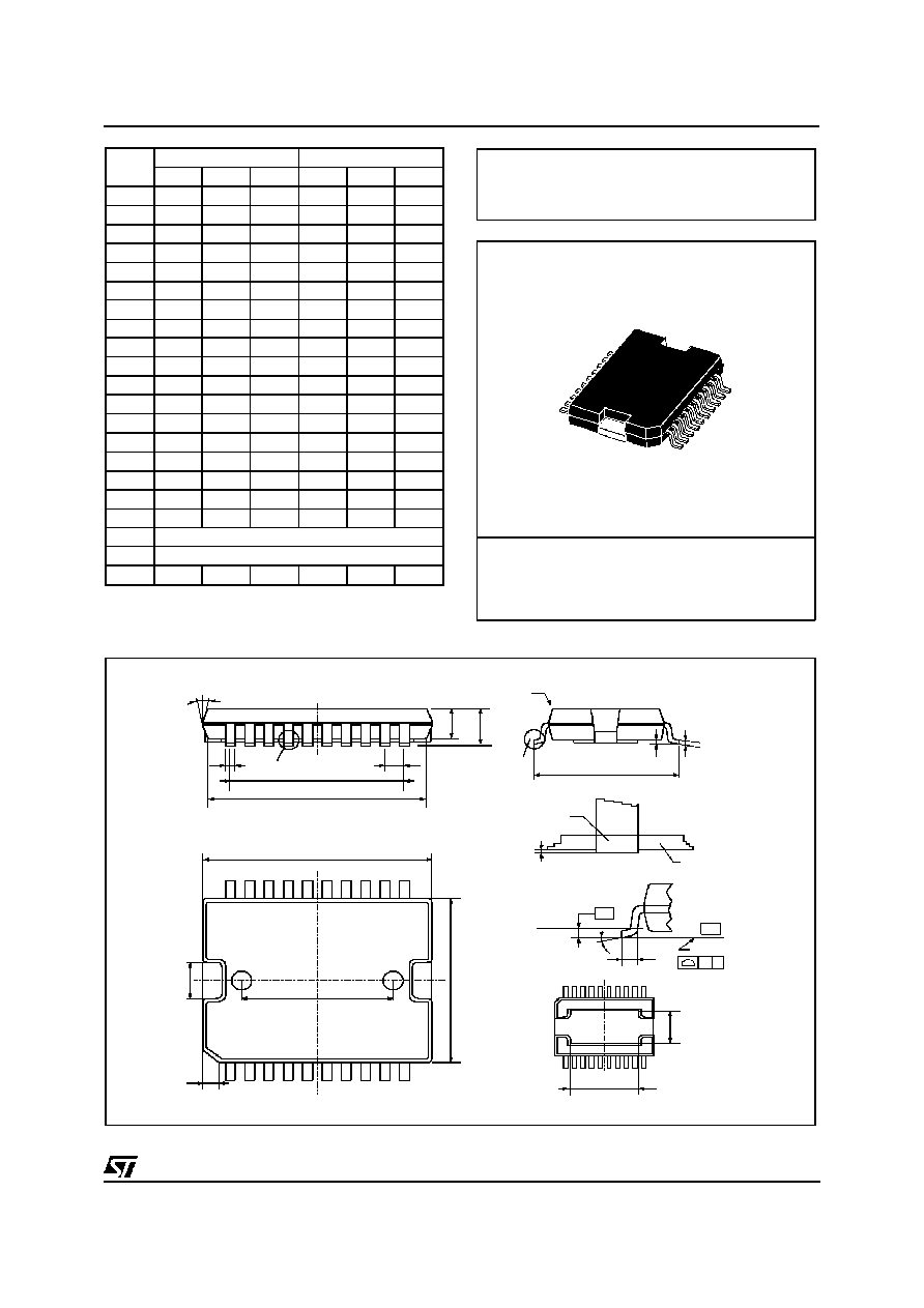
JEDEC MO-166
PowerSO20
e
a2
A
E
a1
PSO20MEC
DETAIL A
T
D
1
11
20
E1
E2
h x 45
DETAIL A
lead
slug
a3
S
Gage Plane
0.35
L
DETAIL B
R
DETAIL B
(COPLANARITY)
G
C
- C -
SEATING PLANE
e3
b
c
N
N
H
BOTTOM VIEW
E3
D1
DIM.
mm
inch
MIN.
TYP.
MAX.
MIN.
TYP.
MAX.
A
3.6
0.142
a1
0.1
0.3
0.004
0.012
a2
3.3
0.130
a3
0
0.1
0.000
0.004
b
0.4
0.53
0.016
0.021
c
0.23
0.32
0.009
0.013
D (1)
15.8
16
0.622
0.630
D1
9.4
9.8
0.370
0.386
E
13.9
14.5
0.547
0.570
e
1.27
0.050
e3
11.43
0.450
E1 (1)
10.9
11.1
0.429
0.437
E2
2.9
0.114
E3
5.8
6.2
0.228
0.244
G
0
0.1
0.000
0.004
H
15.5
15.9
0.610
0.626
h
1.1
0.043
L
0.8
1.1
0.031
0.043
N
10
∞
(max.)
S
T
10
0.394
(1) "D and F" do not include mold flash or protrusions.
- Mold flash or protrusions shall not exceed 0.15 mm (0.006").
- Critical dimensions: "E", "G" and "a3"
OUTLINE AND
MECHANICAL DATA
8
∞
(max.)
10
L4947PD
5/6

Information furnished is believed to be accurate and reliable. However, STMicroelectronics assumes no responsibility for the consequences
of use of such information nor for any infringement of patents or other rights of third parti es which may result from its use. No license is
granted by implication or otherwise under any patent or patent rights of STMicroelectronics. Specification mentioned in this publication are
subject to change without notice. This publication supersedes and replaces all information previously supplied. STMicroelectronics products
are not authorized for use as critical components in life support devices or systems without express written approval of STMicroelectronics.
The ST logo is a registered trademark of STMicroelectronics
©
2000 STMicroelectronics ≠ Printed in Italy ≠ All Rights Reserved
STMicroelectronics GROUP OF COMPANIES
Australia - Brazil - China - Finland - France - Germany - Hong Kong - India - Italy - Japan - Malaysia - Malta - Morocco -
Singapore - Spain - Sweden - Switzerland - United Kingdom - U.S.A.
http://www.st.com
L4947PD
6/6