 | –≠–ª–µ–∫—Ç—Ä–æ–Ω–Ω—ã–π –∫–æ–º–ø–æ–Ω–µ–Ω—Ç: L4948 | –°–∫–∞—á–∞—Ç—å:  PDF PDF  ZIP ZIP |

L4948
QUAD VOLTAGE REGULATOR WITH INHIBIT AND RESET
4 OUTPUTS: 10V (300mA); 8V (400mA); 5V
(600mA); 5V (100mA)
ALL FOUR OUTPUTS ARE LOW DROP
5V (100mA) ST-BY OUTPUT VOLTAGE
EARLY WARNING OUTPUT FOR SUPPLY
UNDERVOLTAGE (LVW)
THERMAL
SHUTDOWN
AND
CURRENT
LIMITATION (FOLDBACK)
REVERSE BATTERY AND LOAD DUMP
PROTECTION
INHIBIT (ON/OFF) AND RESET FUNCTIONS
DESCRIPTION
The L4948 is a quad output low drop voltage
regulator. All four outputs are low drop: 10V at
300mA (V
O1
), 8V at 400mA (V
O2
), 5V at 600mA
(V
O3
) and a 5V st-by line at 100mA (V
O4
).
The IC includes a monitoring circuit to warn if a
low voltage or no voltage condition is occurring.
V
O1,2,3
are off during st-by mode.
The STCAP pin allows the battery voltage to de-
cay slowly giving the
µ
P time to store data. This
IC is designed for supplying microcomputer con-
trolled systems specially in automotive applica-
tions.
June 2000
Æ
BLOCK DIAGRAM
Multiwatt 11
ORDERING NUMBER: L4948
MULTIPOWER BCD TECHNOLOGY
1/9

OPERATING CONDITION
Symbol
Parameter
Value
Unit
V
S
Supply Voltage
-15 to 27
V
I
L
Load Current I
O1
I
O2
I
O3
I
O4
300
400
600
100
mA
mA
mA
mA
THERMAL DATA
Symbol
Parameter
Value
Unit
R
th j-case
Thermal Resistance Junction-case
max
2
∞
C/W
PIN CONNECTION
ABSOLUTE MAXIMUM RATINGS
Symbol
Parameter
Value
Unit
V
S
Supply Voltage
-35 to 60
V
V
I
Input Voltage (ON/OFF)
0 to 12
V
V
O
Output Voltage (LVW, Reset)
0 to 12
V
T
stg
Storage Temperature Range
-65 to 150
∞
C
T
j
Junction Temperature Range
max 150
∞
C
Load Dump (5ms rise, 115ms decay)
60
V
APPLICATION CIRCUIT
L4948
2/9

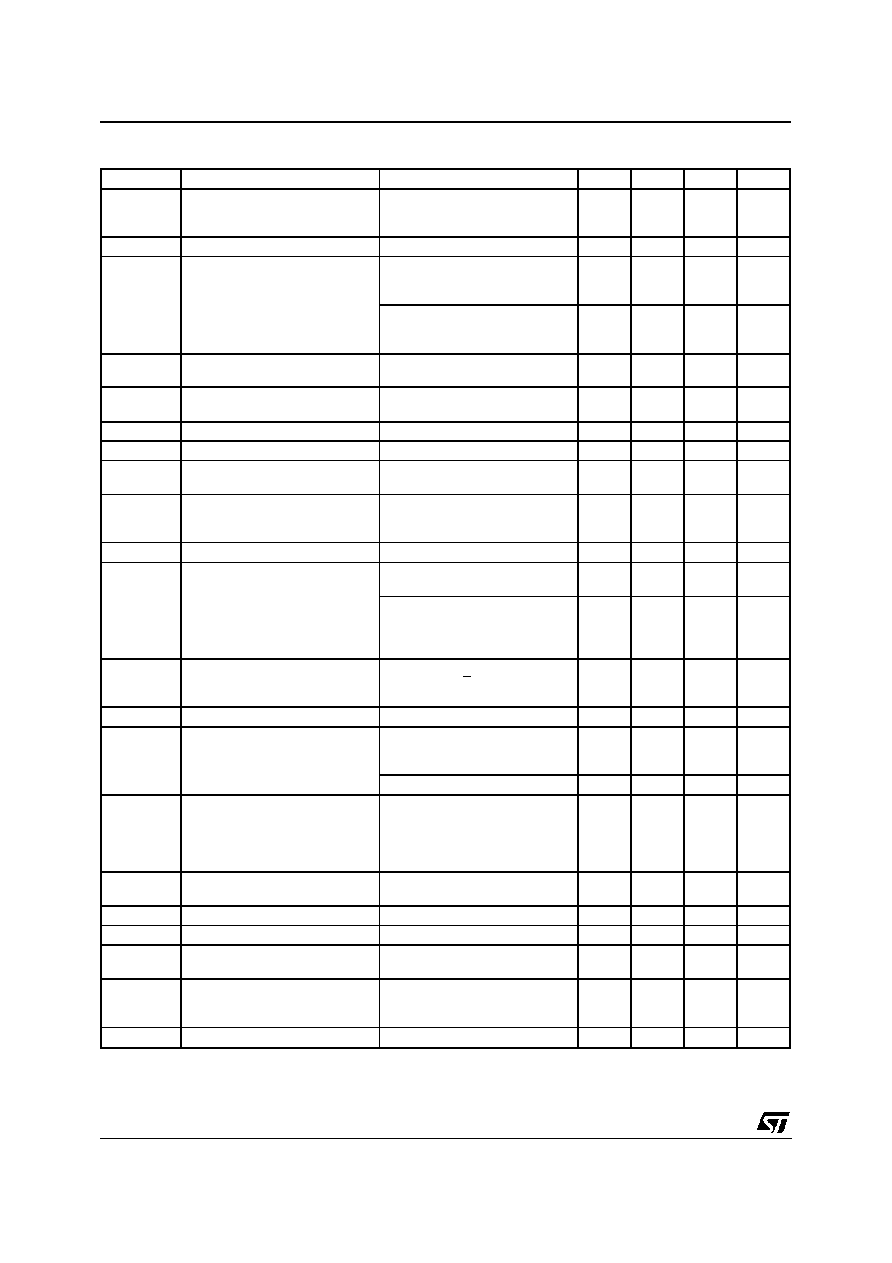
ELECTRICAL CHARACTERISTICS (V
S
= 10.5 to 16V; I
O1
= 6mA, I
O2
= 8mA, I
O3
= 4mA; I
O4
= 0.4mA;
C
O
= 10
µ
F max; T
amb
= -40 to 85
∞
C, unless otherwise specified.)
Symbol
Parameter
Test Condition
Min.
Typ.
Max.
Unit
V
O1
Output Voltage
I
O1
= 300mA; T
amb
= 25
∞
C;
11V < V
S
< 16V all temps
9.7
9.5
10
10
10.3
10.5
V
V
V
O1
Load Regulation
I
O1
= 6 to 300mA
150
mV
I
Q
Quiescent Current (
I
S
)
V
S
= 14V; I
O1
= 6mA;
V
S
=14V ; I
O1
= 300mA;
10
30
mA
mA
V
S
-V
O1
Dropout Voltage
I
O1
= 300mA
T
amb
= 25
∞
C;
all temps
400
600
mV
mV
L
Current Limit (Foldback) note1
V
O1
= 0V
360
800
mA
V
O1
Max Bat.Trans.
R
O
= 100
Ramp V
S
from 14 to 60V in 3-5ms
11
V
Hold V
S
at 60V for 10ms
Ramp V
S
from60 to 14V in 3-5ms;
T
amb
= 25
∞
C;
all temps
9.7
9.5
10
10
2
10.3
10.5
V
V
V
V
O1
Rev. Voltage Trans.
V
S
= -35V; t
1ms; R
O
= 100
Check V
O1
, T
amb
= 25
∞
C;
all temps
9.7
9.5
10
10
10.3
10.5
V
V
V
O1
Rev. Voltage .
V
S
= -15V; R
O
= 100
-0.4
1
V
Ripple rejection
f
O
= 1KHz; 1V
pp
AC ; V
S
=14V
I
O1
= 180mA; I
O2
= 200mA
;
I
O3
= 400mA; I
O4
= 40mA;
50
dB
f
O
= 10KHz; 1V
pp
AC ; V
S
=14V
I
O1
= 180mA; I
O2
= 200mA
;
I
O3
= 400mA; I
O4
= 40mA;
50
dB
V
O1
Line Regulation
V
O1
across V
S
range
V
S
= 11V to 26V
50
mV
Output Noise
Check Output for AC noise
using a 100KHz LP filter
Check Output for AC noise
using an A weighted filter (20-
20KHz)
400
200
µ
V
µ
V
V
O2
Output Voltage
I
O2
= 400mA; T
amb
= 25
∞
C;
all temps
7.75
7.60
8
8
8.25
8.40
V
V
V
O2
Load Regulation
I
O2
= 8 to 400mA
150
mV
I
Q
Quiescent Current (
I
S
)
V
S
= 14V; I
O2
= 8mA;
V
S
= 14V; I
O2
= 400mA;
10
35
mA
mA
V
S
-V
O2
Dropout Voltage
I
O2
= 400mA
set V
S
= V
O2
+1V; T
amb
= 25
∞
C;
set V
S
= V
O2
+1.5V;all temps
400
600
mV
mV
L
Current Limit (Foldback) note1
V
O2
= 0V
480
960
mA
V
O2
Max Bat.Trans.
R
O
= 100
Ramp V
S
from 14 to 60V in 3-5ms
9
V
Hold V
S
at 60V for 10ms
Ramp V
S
from60 to 14V in 3-5ms;
T
amb
= 25
∞
C;
all temps
7.75
7.60
8
8
2
8.25
8.40
V
V
V
L4948
3/9
ELECTRICAL CHARACTERISTICS (continued)
Symbol
Parameter
Test Condition
Min.
Typ.
Max.
Unit
V
O2
Rev. Voltage Trans.
V
S
= -35V; R
O
= 100
t
1ms
Check V
O2
, standard T
amb
= 25
∞
C;
all temps
7.75
7.60
8
8
8.25
8.40
V
V
V
O2
Rev. Voltage .
V
S
= -15V; t = 30s; R
O
= 100
-0.4
1
V
Ripple rejection
f
O
= 1KHz; 1V
pp
AC ; V
S
=14V
I
O1
= 180mA; I
O2
= 200mA
;
I
O3
= 400mA; I
O4
= 40mA;
50
dB
f
O
= 10KHz; 1V
pp
AC ; V
S
=14V
I
O1
= 180mA; I
O2
= 200mA
;
I
O3
= 400mA; I
O4
= 40mA;
50
dB
V
O2
Line Regulation
V
O2
across V
S
range
V
S
= 10.5V to 26V
40
mV
V
O3
Output Voltage
I
O3
= 600mA; T
amb
= 25
∞
C;
all temps
4.85
4.75
5
5
5.15
5.25
V
V
V
O3
Line Regulation
V
S
= 7V to 26V
40
mV
V
O3
Load Regulation
I
O3
= 4 to 600mA
100
mV
I
Q
Quiescent Current (
I
S
)
V
S
= 14V; I
O3
= 4mA;
V
S
= 14V; I
O3
= 600mA;
8
40
mA
mA
V
S
-V
O3
Dropout Voltage
I
O3
= 600mA
set V
S
= V
O3
+1V; T
amb
= 25
∞
C;
set V
S
= V
O3
+1.5V;all
400
600
mV
mV
I
L
Current Limit (Foldback) note 1
V
O3
= 0V
720
1440
mA
V
O3
Max Bat.Trans.
R
O
= 100
Ramp V
S
from 14 to 60V in 3-5ms
6
V
Hold V
S
at 60V for 10ms
Ramp V
S
from60 to 14V in 3-5ms;
T
amb
= 25
∞
C;
all temps
4.85
4.75
5
5
2
5.15
5.25
V
V
V
V
O3
Rev. Voltage Trans.
V
S
= -35V; t < 1ms; R
O
= 100
Check V
O3
, standard T
amb
= 25
∞
C;
all temps
4.85
4.75
5
5
5.15
5.25
V
V
V
O3
Rev. Voltage .
V
S
= -15V; R
O
= 100
-0.4
1
V
Ripple rejection
f
O
= 1KHz; 1V
pp
AC ; V
S
=14V
I
O1
= 180mA; I
O2
= 200mA
;
I
O3
= 400mA; I
O4
= 40mA;
50
dB
f
O
= 10KHz; 1V
pp
AC ; V
S
=14V
50
dB
Output Noise
Check Output for AC noise
using a 100KHz LP filter
Check Output for AC noise
using an A weighted filter (20-
20KHz)
400
200
µ
V
µ
V
V
O4
Output Voltage
I
O4
= 100mA; T
amb
= 25
∞
C;
all temps
4.85
4.75
5
5
5.15
5.25
V
V
V
O4
Line Regulation
V
S
= 7V to 26V
40
mV
V
O4
Load Regulation
I
O4
= 0.4 to 100mA
80
mV
I
Q
Quiescent Current
V
S
= 14V; I
O4
= 2mA;
V
S
= 14V; I
O4
= 100mA;
450
20
µ
A
mA
V
S
-V
O4
Dropout Voltage
I
O4
= 100mA
set V
S
= V
O4
+0.5V; T
amb
= 25
∞
C;
set V
S
= V
O4
+0.8V;all temps
400
600
mV
mV
L
Current Limit (Foldback) note 1
V
O4
= 0V
150
300
mA
L4948
4/9

ELECTRICAL CHARACTERISTICS (continued)
Symbol
Parameter
Test Condition
Min.
Typ.
Max.
Unit
V
O4
Max Bat.Trans.
R
O
= 100
0
Ramp V
S
from 14 to 60V in 3-5ms
6
V
Hold V
S
at 60V for 10ms
Ramp V
S
from60 to 14V in 3-5ms;
T
amb
= 25
∞
C;
all temps
4.85
4.75
5
5
6
5.15
5.25
V
V
V
V
O4
Rev. Voltage Trans.
V
S
= -35V; t < 1ms; R
O
= 100
0
Check V
O4
, standard T
amb
= 25
∞
C;
all temps
4.85
4.75
5
5
5.15
5.25
V
V
V
O4
Rev. Voltage .
V
S
= -15V; R
O
= 1000
-0.4
1
V
Ripple rejection
f
O
= 1KHz; 1V
pp
AC ; V
S
=14V
I
O1
= 180mA; I
O2
= 200mA
;
I
O3
= 400mA; I
O4
= 40mA;
50
dB
f
O
= 10KHz; 1V
pp
AC ; V
S
=14V
I
O1
= 180mA; I
O2
= 200mA
;
I
O3
= 400mA; I
O4
= 40mA;
50
dB
Output Noise
Check Output for AC noise
using a 100KHz LP filter
Check Output for AC noise
using an A weighted filter (20-
20KHz)
400
200
µ
V
µ
V
ON/OFF
Input Current
V
S
= 14V; V
IH
= >2V;
V
S
= 14V; V
IL
= <0.8V;
-10
1
µ
A
µ
A
V
I ON/OFF
Input Threshold
V
S
= 14V V
IL
V
S
= 14V V
IH
0
2
0.8
12
V
V
V
R
Reset Output Voltage Set
V
S
so that V
O4
< 4.5V;
R
O
= 200K
to V
04
; V
IL
= "0"
0
0.75
V
V
S
so that V
O4
-0.15V;
R
O
= 200K
to V
04
; V
IH
= "1"
2.75
5
V
LVW and Reset fall Time Set
Measured from 90% to 10%
150
µ
s
LVW and Reset Rise Time
Measured from 90% to 100%
300
µ
s
LVW Output Threshold
Ramp V
S
down until LVW
switches from"1" to a "0"
7.0
8.2
V
LVW Output Voltage
STCAP <6.5V;R
O
= 200K
to
V
O4
; V
IL
= "0"
0
0.75
V
STCAP >7.5V;R
O
= 200K
to
V
O4
; V
IH
= "1"
2.75
50
V
Reset Output Stability
V
S
is set such that 1 < V
04
<
4V; I
OUT4
= 2mA; V
ON/OFF
= 0
meas reset variation
50
mV
I
q
St-By Quiescent Current (
I
S
)
V
ON/OFF
= 0V
;
I
O 4
= 100mA;
V
S
= 14V; I
O 1,2,3
= 0mA
20
mA
V
ON/OFF
= 0V
;
I
O 4
= 2mA;
V
bat
= 14V; I
O 1,2,3
= 0mA
500
µ
A
Maximum Quiescent Current
(
I
S
)
V
S
= 14V; I
O1
= 300mA;
I
O2
= 400mA
;
I
O3
= 600mA;
I
O4
= 100mA; V
O
= 5V
110
mA
STCAP Output Voltage
V
S
= 24V;
V
S
= 60V. 1ms
15
17
18
V
V
Note 1:
The L4948 has "Foldback" on its outputs during current limiting. As the output loading is increasing the current supplied by the L4948 increases
until a threshold is reached. When the current limiting threshold is reached, the L4948 output current will start to accrease as the loading is
continuoing to increase. The point where the output current stort to decrease is the maximum output current.
L4948
5/9