 | –≠–ª–µ–∫—Ç—Ä–æ–Ω–Ω—ã–π –∫–æ–º–ø–æ–Ω–µ–Ω—Ç: L4957 | –°–∫–∞—á–∞—Ç—å:  PDF PDF  ZIP ZIP |
L4957
UP TO 4A ULDO LINEAR REGULATOR
1.5V AND 2.5V FIXED OUTPUT VOLTAGE
3V TO 6.5V INPUT VOLTAGE RANGE
200m
Rdson TYPICAL @ T
j
= 125
∞
C
0.6V max. DROP-OUT AT 2A
EXCELLENT LOAD REGULATION
0.6mA QUIESCENT CURRENT AT ANY LOAD
SHORT CIRCUIT PROTECTION WITH FOLD-
BACK
THERMAL SHUTDOWN
APPLICATIONS
MOTHER BOARDS
PROCESSOR I/O & SUPPLIES
LOW VOLTAGE MEMORY & CHIP SET SUP-
PLIES
GRAPHIC & SOUND CARDS
LOW VOLTAGE LOGIC SUPPLIES
POST REGULATOR FOR SMPS
DESCRIPTION
The L4957 devices are Ultra Low Drop Output lin-
ear regulators with an internal N-channel MOS of
200m
particulary suitable for low voltage/low
dropout applications.
Operating with a input voltage from 3V to 6.5V
they are capable to deliver up to 4A at 1.5V or
2.5V fixed output voltages.
The devices are ideal for use as one of the sup-
plies required by processor, for example they are
the cost effective and efficient solution for conver-
sion from 3.3V (rail bus) to 2.5V @ 2.5A or to
1.5V with high current rating.
Fast response transient minimise the output ca-
pacitor value. A minimum of 22
µ
F assures the
stability in all load conditions.
The on-chip trimming technique offers a tighter
voltage reference tolerance (with
±
2% including
line and load variation) beside to ensure a con-
trolled short circuit current. Thermal shutdown
provides protection against overload conditions
that creates excessive junction temperature.
February 2000
Æ
L4957
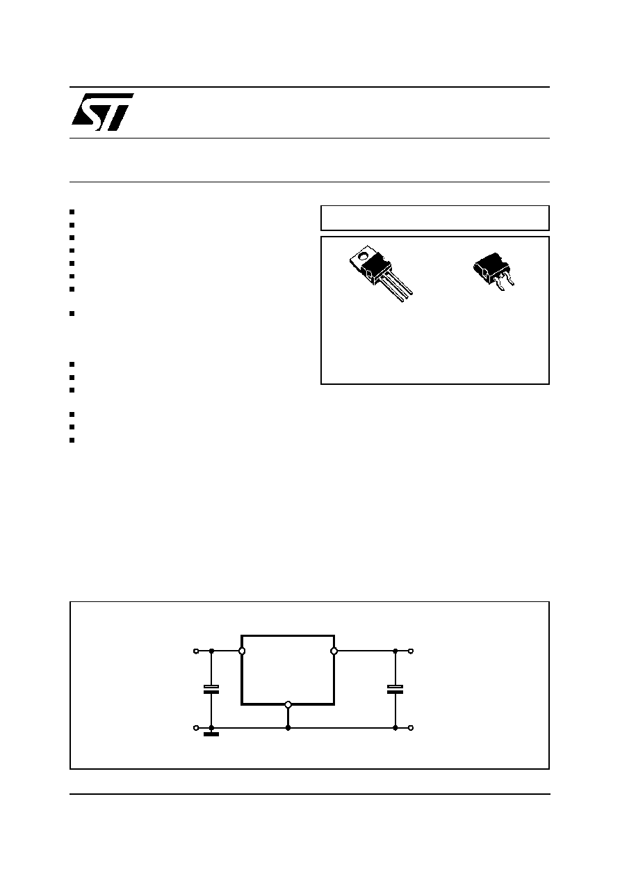
GND
OUT
IN
3
2
1
C1
3V to 6.5V
C2
V
OUT
=1.5V/2.5V
D97IN657E
TYPICAL APPLICATION
ORDERING NUMBERS:
L4957V1.5
L4957D1.5
L4957V2.5
L4957D2.5
MULTIPOWER BCD TECHNOLOGY
1
3
D
2
PAK
Versawatt TO-220
1/7

ABSOLUTE MAXIMUM RATINGS
Symbol
Parameter
Value
Unit
V
IN
Supply Input Voltage
7
V
T
i
Junction Temperature
-40 to +150
∞
C
T
stg
Storage Temperature
-40 to +150
∞
C
PINS CONNECTION
IN
PRE
REGULATOR
V
REF
+
-
E/A
OUT
GND
D98IN839C
1
2
3
V
IN
10
µ
F
CURRENT
LIMIT
WITH
FOLDBACK
THERMAL
SHUTDOWN
BUFFER
CHARGE
PUMP
POWER
DMOS
150m
22
µ
F
V
OUT
R
Y
R
X
BLOCK DIAGRAM
OUT
GND
IN
1
3
D98IN838B
2
Versawatt (TO220)
OUT
GND
IN
1
3
D98IN933A
2
D2PAK
L4957
2/7

L4957 - ELECTRICAL CHARACTERISTICS (T
j
= 25
∞
C, V
IN
= 5V, unless otherwise specified).
∑
= Specifications referred to T
J
from 0
∞
C to +125
∞
C.
Symbol
Parameter
Test Condition
Min.
Typ.
Max.
Unit
V
IN
Operating Supply Voltage
(1)
3
6.5
V
V
O
Output Voltage (1)
For L4957V1.5/D1.5
0.1A < I
O
< 4A; 3V < V
IN
< 6.5V
3V < V
IN
< 6.5V; 0.1A < I
O
< 4A
∑
1.47
1.455
1.5
1.5
1.53
1.545
V
V
For L4957V2.5/D2.5
0.1A < I
O
< 4A; 3V < V
IN
< 6.5V
3V < V
IN
< 6.5V; 0.1A < I
O
< 4A
∑
2.45
2.425
2.5
2.5
2.55
2.575
V
V
V
O
Load regulation (1)
0.1A < IO < 4A
2
10
mV
R
DSON
Drain-Source ON
Resistance
∑
200
300
m
I
O
Current Limiting
90% V
O
∑
5.1
6.3
7.5
A
Short Circuit Current
V
O
= 0V
∑
1.8
A
I
Q
Quiescent Current
0.1A < I
O
< 4A 3V < V
IN
< 6.5V
∑
0.5
2
mA
Ripple Rejection
f = 120Hz, I
O
= 4A
V
IN
= 5V
V
IN
= 2V
PP
60
75
dB
(1) GND connected to ground.
THERMAL DATA
Symbol
Parameter
TO220
D2PAK
Unit
R
th j-case
Thermal Resistance Junction-case
Max.
2.5
3
∞
C/W
R
th j-amb
Thermal Resistance Junction-ambient
Max.
50
60
∞
C/W
Thermal Shutdown
Typ.
150
∞
C
Thermal Hysteresis
Typ.
20
∞
C
PIN FUNCTIONS
Pin N
∞
Name
Function
1
IN
Unregulated input voltage; this pin must be bypassed with a capacitor larger than 10
µ
F.
2
GND
To connect to Ground to get 1.5V or 2.5V output.
3
OUT
Regulated output voltage. A minimum bypass capacitor of 22
µ
F is required to insure stability.
-40
-20
0
20
40
60
80
100 120 140 160
0
0.5
1
1.5
2
2.5
3
3.5
4
4.5
5
Tj [
∞
C]
Output
Voltage
Deviation
[mV]
3V < Vin < 6.5V
Iout = 10mA
Figure 1: Line Regulation vs. Junction
Temperature
0
1
2
3
4
5
-5
-4
-3
-2
-1
0
1
2
3
4
5
Iout [A]
Output
Voltage
Deviation
[mV]
Vin = 5V
Tj = 25
∞
C
(Pulsed technique has been used)
Vout = 1.5V
Figure 2: Load Regulation
L4957
3/7

*P ulsed tecnique ha s been used
-4 0
-2 0
0
2 0
4 0
6 0
80
10 0 1 20 14 0 1 60
0
1
2
3
4
5
6
7
8
9
10
Tj [
∞
C]
O utp ut C urre n t [A]
(Vin-Vout) > 2 V
p in 2 = G ND
Figure 3: Maximum Output Current vs. Junction
Temperature
V in > 2 . 8V
T j= 1 2 5C
Tc =2 5
∞
C
P dm a x = 40 W
R d s on
lim it
D C O p e rat in g A re a
P ow er D is s ip at ion Lim it
C u rre nt L im it a t io n
Tc = 70
∞
C
P d m a x =2 2 W
0
1
2
3
4
5
6
7
8
0
1
2
3
4
5
6
7
8
( Vi n - Vo u t ) [ V ]
O u t p u t C u r r e n t [ A ]
Figure 4: DC Operating Area
0
1 0
2 0
3 0
4 0
5 0
6 0
7 0
8 0
9 0
1 0 0
F r e q u e n c y [ H z ]
R ip p le R e je c t i o n [ d B ]
1 k
1 0
1 0 0
1 0 k
1 0 0 k
V r ip p l e = 3 V p - p V r ipp l e = 0 .5 V p - p
C i n = 2 2u F
C o u t= 2 2 u F
V o u t= 1 . 5 V
V i n m in = 3 V
Io u t= 5 A
Figure 5: Ripple Rejection vs. Frequency
1.8
6.3
IOUT(A)
V
OUT
(V)
D98IN846A
80% V
OUT
Figure 6: Output Voltage vs. Output Current.
(V
OUT
= 1.5V)
0
0 .2 0 .4
0 .6 0 .8
1
1 .2 1 .4 1 .6 1 .8
2
0
0 .5
1
1 .5
2
2 .5
3
3 .5
4
4 .5
5
V = V in - Vo
Io [A ]
m a x im u m R o n l im i ts
T j = 1 0 0
∞
C
T j = 1 2 5
∞
C
T j = 2 5
∞
C
Figure 7: Maximum Output Current vs. Drop-Out
Voltage
L4957
4/7
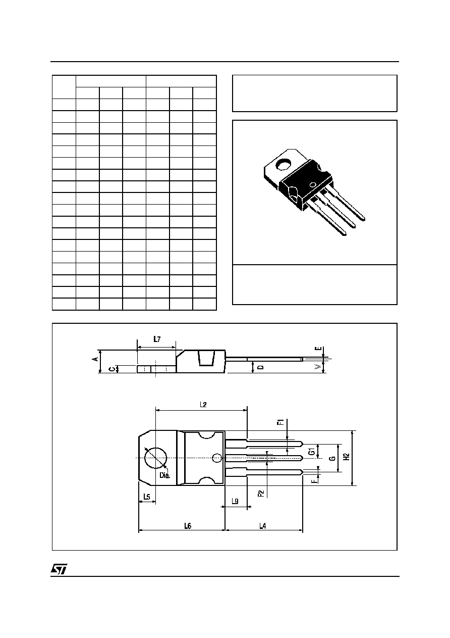
Versawatt (TO220)
DIM.
mm
inch
MIN.
TYP.
MAX.
MIN.
TYP.
MAX.
A
4.40
4.60
0.173
0.181
C
1.23
1.32
0.048
0.051
D
2.40
2.72
0.094
0.107
E
0.49
0.70
0.019
0.027
F
0.61
0.88
0.024
0.034
F1
1.14
1.70
0.044
0.067
F2
1.14
1.70
0.044
0.067
G
4.95
5.15
0.194
0.203
G1
2.40
2.70
0.094
0.106
H2
10.0
10.4
0.393
0.409
L2
16.4
0.645
L4
13.0
14.0
0.511
0.551
L5
2.65
2.95
0.104
0.116
L6
15.25
15.75
0.600
0.620
L7
6.20
6.60
0.244
0.260
L9
3.50
3.93
0.137
0.154
M
2.6
0.102
Dia
3.75
3.85
0.147
0.151
M
TO220MEC
OUTLINE AND
MECHANICAL DATA
L4957
5/7

D
2
PAK
OUTLINE AND
MECHANICAL DATA
A
C2
D
R
2.0 MIN.
FLAT ZONE
A2
V2
C
A1
G
L
L3
L2
B
B2
E
8.90
3.70
1.30
5.08
16.90
10.30
REF.
DIMENSIONS
Millimeters
Inches
Min.
Typ.
Max.
Min.
Typ.
Max.
A
4.30
4.60 0.169
0.181
A1
2.49
2.69 0.098
0.106
A2
0.03
0.23 0.001
0.009
B
0.70
0.93 0.027
0.037
B2
1.25
1.40
0.049 0.055
C
0.45
0.60 0.017
0.024
C2
1.21
1.36 0.047
0.054
D
8.95
9.35 0.352
0.368
E
10.00
10.28 0.393
0.405
G
4.88
5.28 0.192
0.208
L
15.00
15.85 0.590
0.624
L2
1.27
1.40 0.050
0.055
L3
1.40
1.75 0.055
0.069
R
0.40
0.016
V2
0
∞
8
∞
0
∞
8
∞
L4957
6/7

Information furnished is believed to be accurate and reliable. However, STMicroelectronics assumes no responsibility for the consequences
of use of such information nor for any infringement of patents or other rights of third parti es which may result from its use. No license is
granted by implication or otherwise under any patent or patent rights of STMicroelectronics. Specification mentioned in this publication are
subject to change without notice. This publication supersedes and replaces all information previously supplied. STMicroelectronics products
are not authorized for use as critical components in life support devices or systems without express written approval of STMicroelectronics.
The ST logo is a registered trademark of STMicroelectronics
©
2000 STMicroelectronics ≠ Printed in Italy ≠ All Rights Reserved
STMicroelectronics GROUP OF COMPANIES
Australia - Brazil - China - Finland - France - Germany - Hong Kong - India - Italy - Japan - Malaysia - Malta - Morocco -
Singapore - Spain - Sweden - Switzerland - United Kingdom - U.S.A.
http://www.st.com
L4957
7/7