 | –≠–ª–µ–∫—Ç—Ä–æ–Ω–Ω—ã–π –∫–æ–º–ø–æ–Ω–µ–Ω—Ç: L4959 | –°–∫–∞—á–∞—Ç—å:  PDF PDF  ZIP ZIP |
L4959
MULTIFUNCTION VOLTAGE REGULATOR FOR HOME AUDIO
4 OUTPUTS:
12V (1.3A); 12V (0.8A); 8.6V (0.6A); 5.6V
(0.25A) STANDBY
OUT1 12V(a), OUT2 12V(b) AND OUT3 8.6V
WITH INDEPENDENT ENABLE CONTROL
FOR STAND-BY MODE
SHORT-CIRCUIT PROTECTION TO GROUND
THERMAL SHUTDOWN
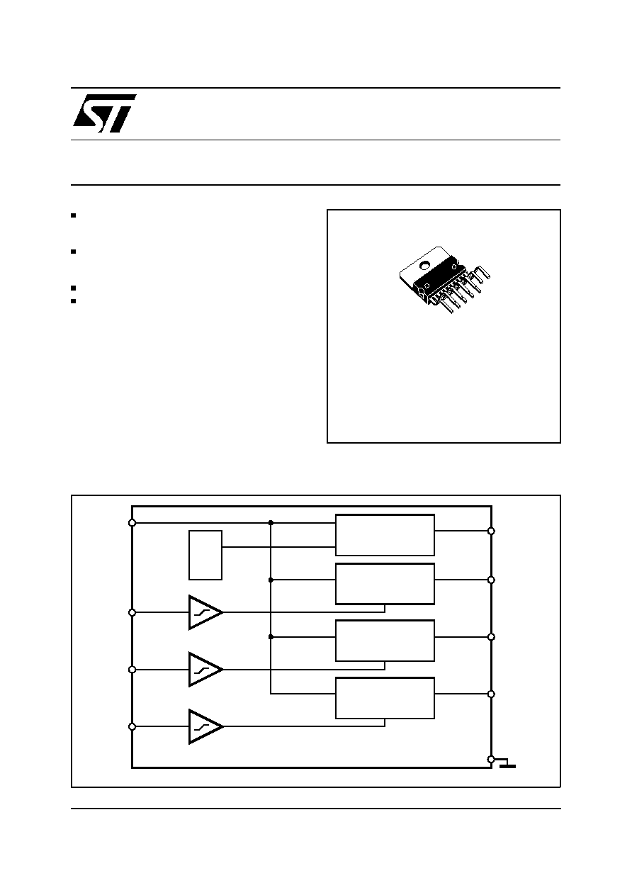
DESCRIPTION
The L4959 is a monolithic Multifunction Voltage
Regulator, designed mainly for supplying Home
Audio systems. The L4959 contains one un-
switched linear 5.6V regulator for Micro, two
switched regulators 8.6V and 12V, suitable to
feed CD or CD players and LED, Signal Process.
An additional 12V regulator for Solenoid Motor an
CD_TRAY Driven is also available.
January 1999
Æ
5.6V, 250mA
REGULATOR
REF
GEN
8.6V, 600mA
REGULATOR
SWITCHED
12V, 800mA
REGULATOR
SWITCHED
12V, 1.3A
REGULATOR
SWITCHED
VS
2/10
GND
6
EN 8V
8
EN 12V(a)
7
EN 12V(b)
5
3
OUT 5.6V
9
OUT 8.6V
11
OUT 12V(a)
1
OUT 12V(b)
D97AU569C
BLOCK DIAGRAM
Multiwatt 11
ORDERING NUMBER: L4959
1/6

ABSOLUTE MAXIMUM RATINGS
Symbol
Parameter
Value
Unit
V
S
DC Supply Voltage
35
V
I
O
Output Current
internally limited
T
op
Operating Temperature Range
0 to +70
∞
C
T
stg
Storage Temperature
≠40 to 150
∞
C
QUICK REFERENCE DATA
Symbol
Parameter
Test Condition
Typ.
Unit
V
out 5V
5V Output Voltage
IO = 125mA
5.6
V
14.4V < V
S
< 21.6V
5mA < I < 0.25A
5.6
V
V
out 8V
8.6V Output Voltage
IO = 300mA
8.6
V
14.4V < V
S
< 21.6V 5mA < I < 0.6A
8.6
V
V
out 12Va
12V Output Voltage
Iout = 400mA
12
V
14.4V < V
S
< 21.6V
5mA < I < 0.8A
12
V
V
out 12Vb
12V Output Voltage
Iout = 650mA
12
V
14.4V < V
S
< 21.6V 5mA < I < 1.3A
12
V
1
2
3
4
5
6
7
9
10
11
8
OUT 12V(a)
V
S
OUT 8.6V
EN 8.6V
EN 12V(a)
GND
EN 12V(b)
N.C.
OUT 5.6V
V
S
OUT 12V(b)
TAB CONNECTED TO PIN 6
D97AU716A
PIN CONNECTION (Top view)
PIN DESCRIPTION
Pin
Pins
Description
1
OUT 12V (b)
12V/1.3A SWITCHED OUTPUT VOLTAGE
2
V
S
Supply Voltage
3
OUT 5.6V
5.6V/250mA OUTPUT VOLTAGE
4
N.C.
not connected
5
EN 12V (b)
Enable 12V/1.3A SWITCHED OUTPUT VOLTAGE
6
GND
Ground
7
EN 12V (a)
Enable 12V/0.8A SWITCHED OUTPUT VOLTAGE
8
EN 8.6V
Enable 8.6V/0.6A SWITCHED OUTPUT VOLTAGE
9
OUT 8.6
8.6V/0.6A SWITCHED OUTPUT VOLTAGE
10
V
S
Supply Voltage
11
OUT 12V (a)
12V/0.8A SWITCHED OUTPUT VOLTAGE
L4959
2/6

THERMAL DATA
Symbol
Parameter
Value
Unit
R
th j-case
Thermal Resistance Junction-case
2
∞
C/W
ELECTRICAL CHARACTERISTICS (V
S
= 18V, T
case
= 25
∞
C, unless otherwise specified.)
Symbol
Parameter
Test Condition
Min.
Typ.
Max.
Unit
V
S
Operating Supply Voltage
no load
15
22
30
V
loaded (*)
14.4
18
21.6
V
En
Output Noise Voltage
Any reg. supply,
f = 100Hz to 20KHz
200
400
µ
V
I
q
Quiescent Current
8
mA
5.6V/250mA OUTPUT VOLTAGE
V
out 5V
5V Output Voltage
I
O
= 125mA
5.45
5.9
V
14.4V < V
S
< 21.6V
5mA < I < 0.25
5.40
6
V
V
line
Line Regulation
14.4V < V
S
< 21.6V
5
50
mV
V
load
Load Regulation
5mA < Io < 250mA
50
150
mV
V
dropout
Dropout Voltage
I
out
= 250mA
2.05
2.7
V
I
lim
Current Limit
V
S
= 21.6V
250
325
mA
8.6V/0.6A SWITCHED OUTPUT VOLTAGE
V
out 8V
8.6V Output Voltage
I
O
= 300mA
8.4
9.1
V
14.4V < V
S
< 21.6V 5mA < I < 0.6A
8.3
9.2
V
V
line
Line Regulation
14.4V < V
S
< 21.6V
5
50
mV
V
load
Load Regulation
5mA < Io < 0.6A
50
350
mV
V
dropout
Dropout Voltage
I
out
= 0.6A
2.05
2.7
V
I
lim
Current Limit
V
S
= 21.6V
0.6
0.8
A
SWon
Switch ON
2.31
3.5
V
SW off
Switch OFF
1.5
2.11
V
SW hyst
Switch Hysteresis
200
mV
12V/0.8A SWITCHED OUTPUT VOLTAGE
V
out12Va
12V Output Voltage
I
out
= 400mA
11.7
12.7
V
14.4V < V
S
< 21.6V
5mA < I < 0.8A
11.6
12.8
V
V
line
Line Regulation
14.4V < Vs < 21.6V
10
50
mV
V
load
Load Regulation
5mA < Io < 0.8A
100
350
mV
V
dropout
Dropout Voltage
I
out
= 0.8A
2.13
2.7
V
I
lim
Current Limit
V
S
= 21.6V
0.8
1.1
A
SVR
Supply Voltage Rejection
f = 100Hz
f = 10KHz
55
40
75
dB
SWon
Switch ON
2.31
3.5
V
SW off
Switch OFF
1.5
2.11
V
SW hyst
Switch Hysteresis
200
mV
12V/1.3A SWITCHED OUTPUT VOLTAGE
V
out12Vb
12V Output Voltage
I
out
= 650mA
11.6
12.6
V
14.4V < V
S
< 21.6V
5mA < I < 1.3A
11.5
12.7
V
V
line
Line Regulation
14.4V < Vs < 21.6V
10
50
mV
V
load
Load Regulation
5mA < Io < 1.3A
200
450
mV
V
dropout
Dropout Voltage
I
out
= 1.3A
2.15
2.7
V
I
lim
Current Limit
V
S
= 21.6V
1.3
1.7
A
L4959
3/6

Figure 2: PCB and Components layout of the Figure 1.
L4959
C2
0.33
µ
F
C3
0.1
µ
F
C1
2200
µ
F
35VL
+V
S
GND
C4
0.1
µ
F
C5
0.1
µ
F
C6
0.1
µ
F
C7
100
µ
F
16VL
C8
100
µ
F
16VL
C9
100
µ
F
16VL
C10
100
µ
F
16VL
V
CC
G
EN8.6V
EN12Va
EN12Vb
5.6V 0.25A
3
8
7
5
11
1
9
10
2
6
µ
-PROC
SIGNAL
12Va 0.8A
12Vb 1.3A
8.6V 0.6A
DECK
CD
+5V
D97AU802
Figure 1: Application and Test Circuit.
ELECTRICAL CHARACTERISTICS (continued)
Symbol
Parameter
Test Condition
Min.
Typ.
Max.
Unit
SVR
Supply Voltage Rejection
f = 100Hz
f = 10KHz
55
40
75
dB
SWon
Switch ON
2.31
3.5
V
SW off
Switch OFF
1.5
2.11
V
SW hyst
Switch Hysteresis
200
mV
(*) The max value is limited by the power dissipation
L4959
4/6

Multiwatt11 V
DIM.
mm
inch
MIN.
TYP.
MAX.
MIN.
TYP.
MAX.
A
5
0.197
B
2.65
0.104
C
1.6
0.063
D
1
0.039
E
0.49
0.55
0.019
0.022
F
0.88
0.95
0.035
0.037
G
1.45
1.7
1.95
0.057
0.067
0.077
G1
16.75
17
17.25
0.659
0.669
0.679
H1
19.6
0.772
H2
20.2
0.795
L
21.9
22.2
22.5
0.862
0.874
0.886
L1
21.7
22.1
22.5
0.854
0.87
0.886
L2
17.4
18.1
0.685
0.713
L3
17.25
17.5
17.75
0.679
0.689
0.699
L4
10.3
10.7
10.9
0.406
0.421
0.429
L7
2.65
2.9
0.104
0.114
M
4.25
4.55
4.85
0.167
0.179
0.191
M1
4.73
5.08
5.43
0.186
0.200
0.214
S
1.9
2.6
0.075
0.102
S1
1.9
2.6
0.075
0.102
Dia1
3.65
3.85
0.144
0.152
OUTLINE AND
MECHANICAL DATA
L4959
5/6