 | –≠–ª–µ–∫—Ç—Ä–æ–Ω–Ω—ã–π –∫–æ–º–ø–æ–Ω–µ–Ω—Ç: L4960H | –°–∫–∞—á–∞—Ç—å:  PDF PDF  ZIP ZIP |

Æ
L4960
2.5A POWER SWITCHING REGULATOR
2.5A OUTPUT CURRENT
5.1V TO 40V OPUTPUT VOLTAGE RANGE
PRECISE (
±
2%) ON-CHIP REFERENCE
HIGH SWITCHING FREQUENCY
VERY HIGH EFFICIENCY (UP TO 90%)
VERY FEW EXTERNAL COMPONENTS
SOFT START
INTERNAL LIMITING CURRENT
THERMAL SHUTDOWN
DESCRIPTION
The L4960 is a monolithic power switching regula-
tor delivering 2.5A at a voltage variable from 5V to
40V in step down configuration.
Features of the device include current limiting, soft
start, thermal protection and 0 to 100% duty cycle
for continuous operation mode.
June 2000
ORDERING NUMBERS: L4960 (Vertical)
L4960H (Horizontal)
HEPTAWATT
BLOCK DIAGRAM
The L4960 is mounted in a Heptawatt plastic power
package and requires very few external compo-
nents.
Efficient operation at switching frequencies up to
150KHz allows a reduction in the size and cost of
external filter components.
1/16

PIN CONNECTION (Top view)
2/16
N
∞
NAME
FUNCTION
1
SUPPLY VOLTAGE
Unregulated voltage input. An internal regulator powers the
internal logic.
2
FEEDBACK INPUT
The feedback terminal of the regulation loop. The output is
connected directly to this terminal for 5.1V operation; it is
connected via a divider for higher voltages.
3
FREQUENCY
COMPENSATION
A series RC network connected between this terminal and
ground determines the regulation loop gain characteristics.
4
GROUND
Common ground terminal.
5
OSCILLATOR
A parallel RC network connected to this terminal determines the
switching frequency.
6
SOFT START
Soft start time constant. A capacitor is connected between this
terminal and ground to define the soft start time constant. This
capacitor also determines the average short circuit output
current.
7
OUTPUT
Regulator output.
PIN FUNCTIONS
Symbol
Parameter
Value
Unit
V
1
Input voltage
50
V
V
1
- V
7
Input to output voltage difference
50
V
V
7
Negative output DC voltage
-1
V
Negative output peak voltage at t = 0.1
µ
s; f = 100KHz
-5
V
V
3
, V
6
Voltage at pin 3 and 6
5.5
V
V
2
Voltage at pin 2
7
V
I
3
Pin 3 sink current
1
mA
I
5
Pin 5 source current
20
mA
P
tot
Power dissipation at T
case
90
∞
C
15
W
T
j
, T
stg
Junction and storage temperature
-40 to 150
∞
C
ABSOLUTE MAXIMUM RATINGS
L4960
Symbol
Parameter
Test Conditions
Min.
Typ.
Max.
Unit
DYNAMIC CHARACTERISTICS
V
o
Output voltage range
V
i
= 46V
I
o
= 1A
V
ref
40
V
V
i
Input voltage range
V
o
= V
ref
to 36V
I
o
= 2.5A
9
46
V
V
o
Line regulation
V
i
= 10V to 40V V
o
= V
ref
I
o
= 1A
15
50
mV
V
o
Load regulation
V
o
= V
ref
I
o
= 0.5A to 2A
10
30
mV
V
ref
Internal reference voltage
(pin 2)
V
i
= 9V to 46V
I
o
= 1A
5
5.1
5.2
V
V
ref
T
Average temperature
coefficient of refer voltage
T
j
= 0
∞
C to 125
∞
C
I
o
= 1A
0.4
mV/
∞
C
V
d
Dropout voltage
I
o
= 2A
1.4
3
V
I
om
Maximum operating load
current
V
i
= 9V to 46V
V
o
= V
ref
to 36V
2.5
A
I
7L
Current limiting threshold
(pin 7)
V
i
= 9V to 46V
V
o
= V
ref
to 36V
3
4.5
A
I
SH
Input average current
V
i
= 46V; output short-circuit
30
60
mA
Efficiency
f = 100KHz
V
o
= V
ref
75
%
I
o
= 2A
V
o
= 12V
85
%
SVR
Supply voltage ripple
rejection
V
i
= 2V
rms
fripple
= 100Hz
V
o
= V
ref
Io = 1A
50
56
dB
f
Switching frequency
85
100
115
KHz
f
V
i
Voltage stability of
switching frequency
V
i
= 9V to 46V
0.5
%
f
T
j
Temperature stability of
switching frequency
T
j
= 0
∞
C to 125
∞
C
1
%
f
max
Maximum operating
switching frequency
V
o
= V
ref
I
o
= 2A
120
150
KHz
T
sd
Thermal shutdown
junction temperature
150
∞
C
ELECTRICAL CHARACTERISTICS (Refer to the test circuit, T
j
= 25
∞
C, V
i
= 35V, unless otherwise
specified)
Symbol
Parameter
Value
Unit
R
th j-case
Thermal resistance junction-case
max
4
∞
C/W
R
th j-amb
Thermal resistance junction-ambient
max
50
∞
C/W
THERMAL DATA
3/16
L4960
4/16
Symbol
Parameter
Test Conditions
Min.
Typ.
Max.
Unit
DC CHARACTERISTICS
I
1Q
Quiescent drain current
100% duty cycle
pins 5 and 7 open
V
i
= 46V
30
40
mA
0% duty cycle
15
20
mA
-I
7L
Output leakage current
0% duty cycle
1
mA
SOFT START
I
6SO
Source current
100
140
180
µ
A
I
6SI
Sink current
50
70
120
µ
A
ERROR AMPLIFIER
V
3H
High level output voltage
V
2
= 4.7V
I
3
= 100
µ
A
3.5
V
V
3L
Low level output voltage
V
2
= 5.3V
I
3
= 100
µ
A
0.5
V
I
3SI
Sink output current
V
2
= 5.3V
100
150
µ
A
-I
3SO
Source output current
V
2
= 4.7V
100
150
µ
A
I
2
Input bias current
V
2
= 5.2V
2
10
µ
A
G
v
DC open loop gain
V
3
= 1V to 3V
46
55
dB
OSCILLATOR
-I
5
Oscillator source current
5
mA
ELECTRICAL CHARACTERISTICS (continued)
L4960
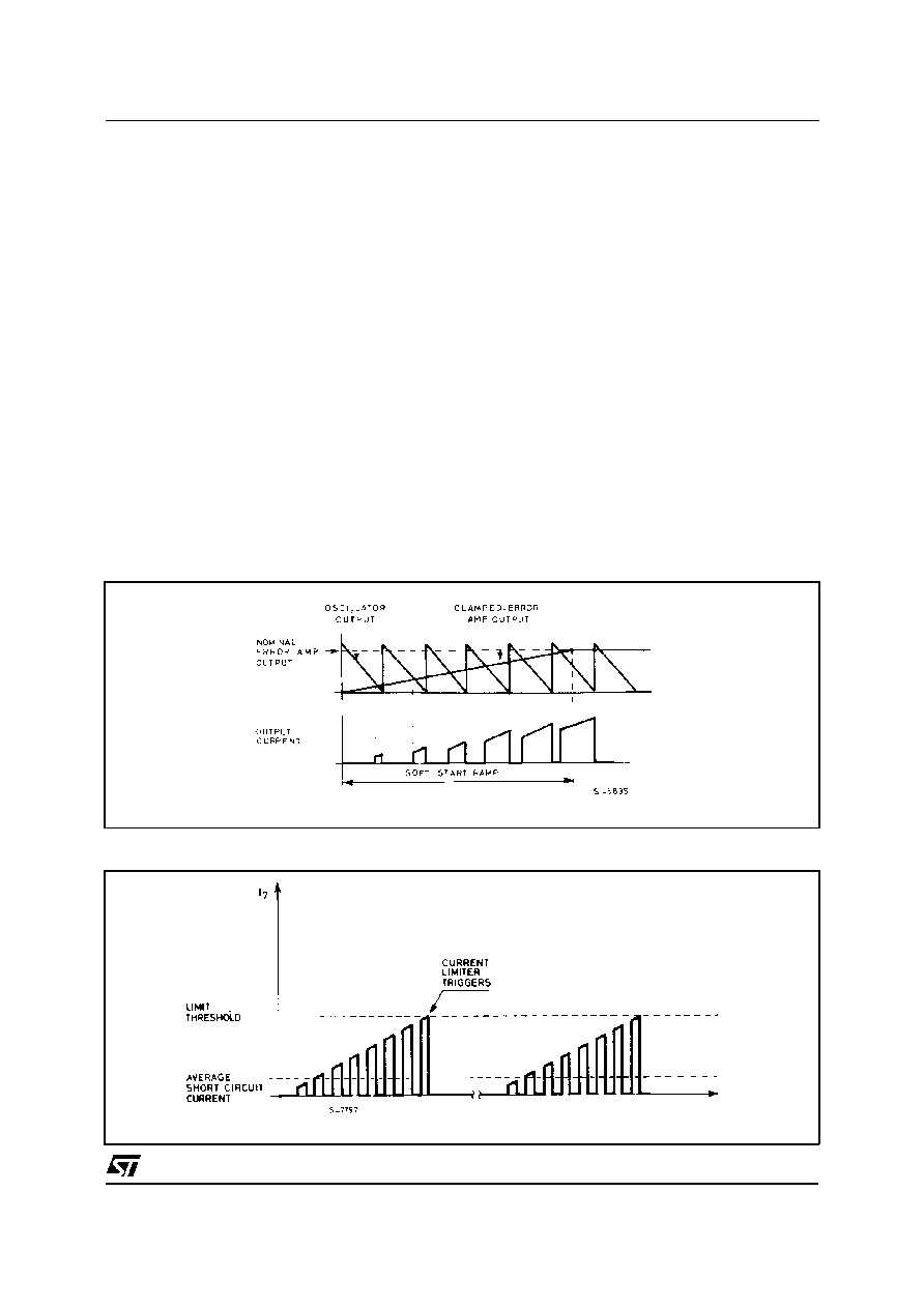
CIRCUIT OPERATION (refer to the block diagram)
The L4960 is a monolithic stepdown switching regu-
lator providing output voltages from 5.1V to 40V and
delivering 2.5A.
The regulation loop consists of a sawtooth oscilla-
tor, error amplifier, comparator and the output
stage. An error signal is produced by comparing the
output voltage with a precise 5.1V on-chip refer-
ence (zener zap trimmed to
±
2%).
This error signal is then compared with the sawtooth
signal to generate the fixed frequency pulse width
modulated pulses which drive the output stage.
The gain and frequency stability of the loop can be
adjusted by an external RC network connected to
pin 3. Closing the loop directly gives an output
voltage of 5.1V. Higher voltages are obtained by
inserting a voltage divider.
Output overcurrents at switch on are prevented by
the soft start function. The error amplifier output is
initially clamped by the external capacitor C
ss
and
allowed to rise, linearly, as this capacitor is charged
by a constant current source. Output overload pro-
tection is provided in the form of a current limiter.
The load current is sensed by an internal metal
resistor connected to a comparator. When the load
current exceeds a preset threshold this comparator
sets a flip flop which disables the output stage and
discharges the soft start capacitor. A second com-
parator resets the flip flop when the voltage across
the soft start capacitor has fallen to 0.4V.
The output stage is thus re-enabled and the output
voltage rises under control of the soft start network.
If the overload condition is still present the limiter
will trigger again when the threshold current is
reached. The average short circuit current is limited
to a safe value by the dead time introduced by the
soft start network. The thermal overload circuit dis-
ables circuit operation when the junction tempera-
ture reaches about 150
∞
C and has hysteresis to
prevent unstable conditions.
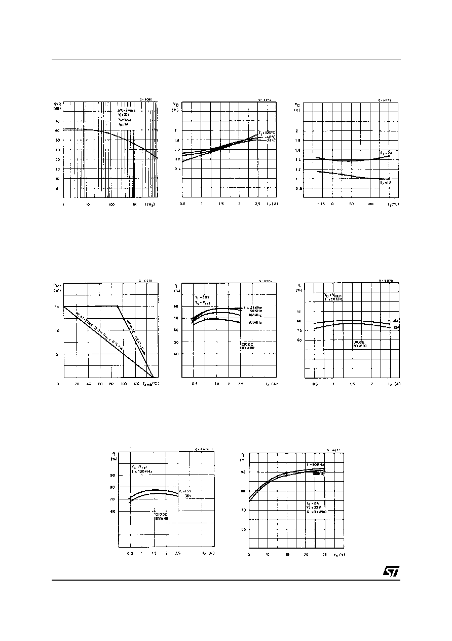
Figure 1. Soft start waveforms
Figure 2. Current limiter waveforms
5/16
L4960

6/16
Figure 4. Quiescent drain
current vs. supply voltage (0%
duty cycle)
Figure 5. Quiescent drain
current vs. supply voltage
(100% duty cycle)
Figure 6. Quiescent drain
current vs. junction tem-
perature (0% duty cycle)
Figure 3. Test and application circuit
C6, C7: EKR (ROE)
L1 = 150
µ
H at 5A (COGEMA 946042)
CORE TYPE: MAGNETICS 58206-A2 MPP
N
∞
TURNS 45, WIRE GAUGE: 0.8mm (20 AWG)
L4960
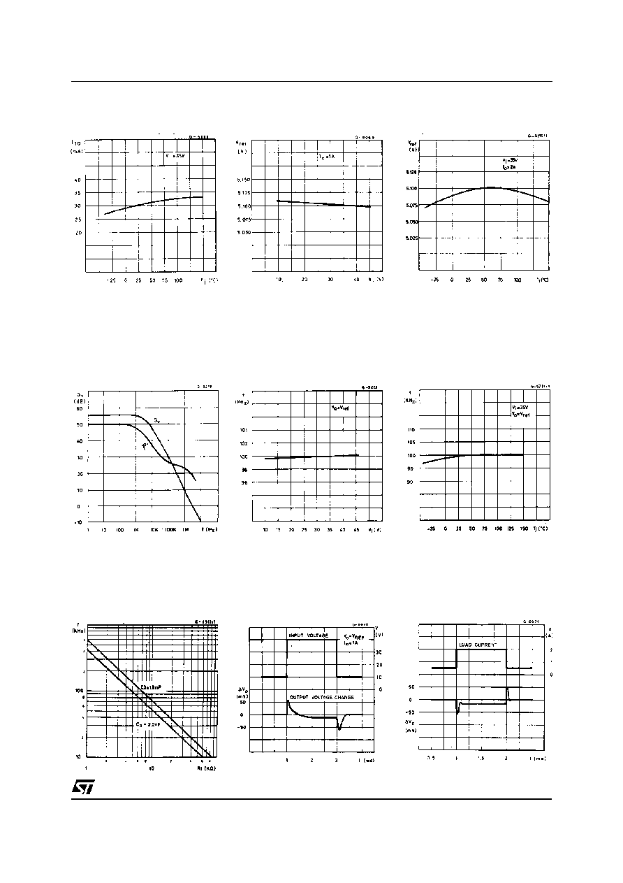
Figure 7. Quiescent drain
current vs. junction tem-
perature (100% duty cycle)
Figure 8. Reference voltage
(pin 2) vs. V
i
Figure 9. Reference voltage
versus junction temperature
(pin 2)
Figure 10. Open loop fre-
quency and phase responde
of error amplifier
Figure 11. Swit ching f re-
quency vs. input voltage
Figure 12. Switching f re-
quency vs. junction tem-
perature
Figure 13. Switching fre-
quency vs. R2 (see test circuit)
Figure 14. Line transient
response
Figure 15. Load transient
response
7/16
L4960
8/16
Figure 16. Supply voltage
ripple rejection vs. frequency
Figure 17. Dropout voltage
between pin 1 and pin 7 vs.
current at pin 7
Figure 18. Dropout voltage
bet ween pin 1 and 7 vs.
junction temperature
Figure 19. Power dissipation
derating curve
Fi gure 20. Ef f ici ency vs.
output current
Fi gure 21 . Ef f i ciency vs.
output current
F igu re 22. E ff i ciency vs.
output current
Fi gure 2 3. E ff i ciency vs.
output voltage
L4960
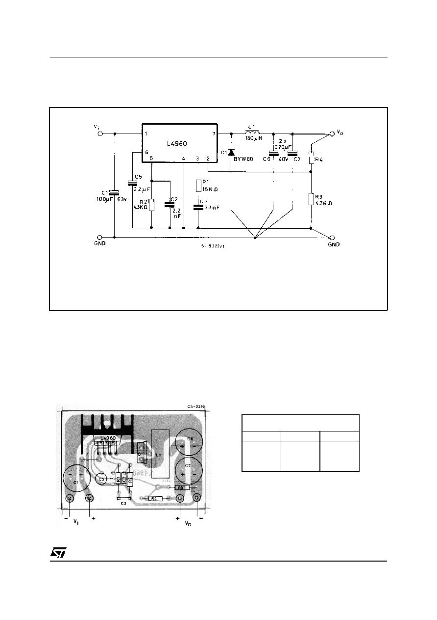
APPLICATION INFORMATION
Figure 24. Typical application circuit
C
1
, C
6
, C
7
: EKR (ROE)
D
1
: BYW80 OR 5A SCHOTTKY DIODE
SUGGESTED INDUCTOR: L
1
= 150
µ
H at 5A
CORE TYPE: MAGNETICS 58206 - A2 - MPP
N
∞
TURNS: 45, WIRE GAUGE: 0.8mm (20 AWG), COGEMA 946042
U15/GUP15: N
∞
TURNS: 60, WIRE GAUGE: 0.8mm (20 AWG), AIR GAP: 1mm, COGEMA 969051.
Figure 25. P.C. board and component layout of
the Fig. 24 (1 : 1 scale)
Resistor values for
standard output voltages
V
o
R3
R4
12V
15V
18V
24V
4.7K
4.7K
4.7K
4.7K
6.2K
9.1K
12K
18K
9/16
L4960

10/16
APPLICATION INFORMATION
Figure 26. A minimal 5.1V fixed regulator; Very few component are required
* COGEMA 946042 (TOROID CORE)
969051 (U15 CORE)
** EKR (ROE)
Figure 27. Programmable power supply
V
o
= 5.1V to 15V
I
o
= 2.5A max
Load regulation (1A to 2A) = 10mV (V
o
= 5.1V)
L4960

APPLICATION INFORMATION (continued)
Figure 28. Microcomputer supply with + 5.1V, -5V, +12V and -12V outputs
11/16
L4960

12/16
APPLICATION INFORMATION (continued)
Figure 29. DC-DC converter 5.1V/4A,
±
12V/2.5A; a suggestion how to synchronize a negative output
L1, L3 = COGEMA 946042 (969051)
L2 = COGEMA 946044 (946045)
D
1
, D
2
, D
3
= BYW80
Figure 30. - In multiple supplies several L4960s can be synchronized as shown
L4960
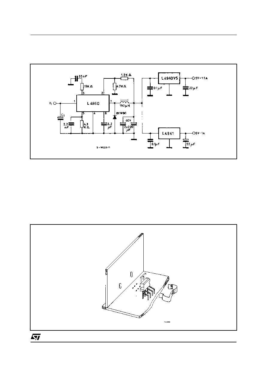
APPLICATION INFORMATION (continued)
Figure 31. Regulator for distributed supplies
MOUNTING INSTRUCTION
The power dissipated in the circuit must be removed
by adding an external heatsink.
Thanks to the Heptawatt package attaching the
hetsink is very simple, a screw or a compression
spring (clip) being sufficient. Between the heatsink
and the package it is better to insert a layer of silicon
grease, to optimize the thermal contact, no electri-
cal isolation is needed between the two surfaces.
Figure 32. Mounting example
13/16
L4960
14/16
Heptawatt V
DIM.
mm
inch
MIN.
TYP.
MAX.
MIN.
TYP.
MAX.
A
4.8
0.189
C
1.37
0.054
D
2.4
2.8
0.094
0.110
D1
1.2
1.35
0.047
0.053
E
0.35
0.55
0.014
0.022
E1
0.7
0.97
0.028
0.038
F
0.6
0.8
0.024
0.031
F1
0.9
0.035
G
2.34
2.54
2.74
0.095
0.100
0.105
G1
4.88
5.08
5.28
0.193
0.200
0.205
G2
7.42
7.62
7.82
0.295
0.300
0.307
H2
10.4
0.409
H3
10.05
10.4
0.396
0.409
L
16.7
16.9
17.1
0.657
0.668
0.673
L1
14.92
0.587
L2
21.24
21.54
21.84
0.386
0.848
0.860
L3
22.27
22.52
22.77
0.877
0.891
0.896
L4
1.29
0.051
L5
2.6
2.8
3
0.102
0.110
0.118
L6
15.1
15.5
15.8
0.594
0.610
0.622
L7
6
6.35
6.6
0.236
0.250
0.260
L9
0.2
0.008
M
2.55
2.8
3.05
0.100
0.110
0.120
M1
4.83
5.08
5.33
0.190
0.200
0.210
V4
40∞ (typ.)
Dia
3.65
3.85
0.144
0.152
A
L
L1
C
D1
L5
L2
L3
D
E
M1
M
H3
Dia.
L7
L6
F1
H2
F
G
G1
G2
E1
F
E
L9
V4
L4
H2
V
V
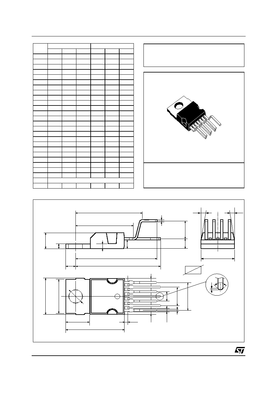
HEPTAMEC
H1
OUTLINE AND
MECHANICAL DATA
L4960
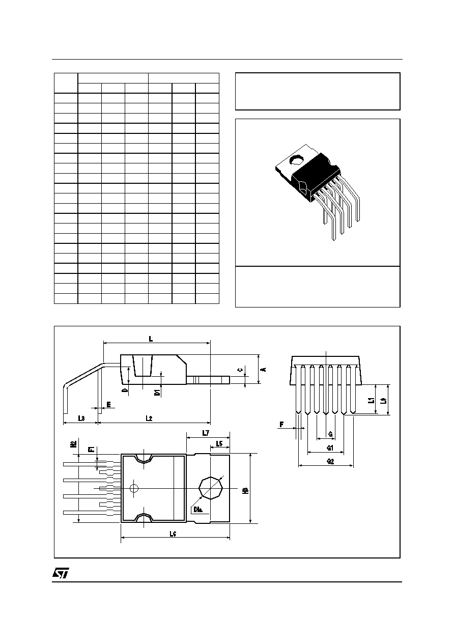
Heptawatt H
DIM.
mm
inch
MIN.
TYP.
MAX.
MIN.
TYP.
MAX.
A
4.8
0.189
C
1.37
0.054
D
2.4
2.8
0.094
0.110
D1
1.2
1.35
0.047
0.053
E
0.35
0.55
0.014
0.022
F
0.6
0.8
0.024
0.031
F1
0.9
0.035
G
2.41
2.54
2.67
0.095
0.100
0.105
G1
4.91
5.08
5.21
0.193
0.200
0.205
G2
7.49
7.62
7.8
0.295
0.300
0.307
H2
10.4
0.409
H3
10.05
10.4
0.396
0.409
L
14.2
0.559
L1
4.4
0.173
L2
15.8
0.622
L3
5.1
0.201
L5
2.6
3
0.102
0.118
L6
15.1
15.8
0.594
0.622
L7
6
6.6
0.236
0.260
L9
4.44
0.175
Dia
3.65
3.85
0.144
0.152
OUTLINE AND
MECHANICAL DATA
15/16
L4960

Information furnished is believed to be accurate and reliable. However, STMicroelectronics assumes no responsibility for the consequences of
use of such information nor for any infringement of patents or other rights of third parties which may result from its use. No license is granted
by implication or otherwise under any patent or patent rights of STMicroelectronics. Specification mentioned in this publication are subject to
change without notice. This publication supersedes and replaces all information previously supplied. STMicroelectronics products are not
authorized for use as critical components in life support devices or systems without express written approval of STMicroelectronics.
The ST logo is a registered trademark of STMicroelectronics
© 2000 STMicroelectronics ≠ Printed in Italy ≠ All Rights Reserved
STMicroelectronics GROUP OF COMPANIES
Australia - Brazil - China - Finland - France - Germany - Hong Kong - India - Italy - Japan - Malaysia - Malta - Morocco -
Singapore - Spain - Sweden - Switzerland - United Kingdom - U.S.A.
http://www.st.com
16/16
L4960