 | –≠–ª–µ–∫—Ç—Ä–æ–Ω–Ω—ã–π –∫–æ–º–ø–æ–Ω–µ–Ω—Ç: L4978D | –°–∫–∞—á–∞—Ç—å:  PDF PDF  ZIP ZIP |

UP TO 2A STEP DOWN CONVERTER
OPERATING INPUT VOLTAGE FROM 8V TO
55V
PRECISE 3.3V (
±
1%) INTERNAL REFER-
ENCE VOLTAGE
OUTPUT VOLTAGE ADJUSTABLE FROM
3.3V TO 50V
SWITCHING FREQUENCY ADJUSTABLE UP
TO 300KHz
VOLTAGE FEEDFORWARD
ZERO LOAD CURRENT OPERATION
INTERNAL CURRENT LIMITING (PULSE-BY-
PULSE AND HICCUP MODE)
INHIBIT FOR ZERO CURRENT CONSUMP-
TION
PROTECTION AGAINST FEEDBACK DIS-
CONNECTION
THERMAL SHUTDOWN
SOFT START FUNCTION
DESCRIPTION
The L4978 is a step down monolithic power
switching regulator delivering 2A at a voltage be-
tween 3.3V and 50V (selected by a simple exter-
nal divider). Realized in BCD mixed technology,
the device uses an internal power D-MOS transis-
tor (with a typical Rdson of 0.25
) to obtain very
high efficency and high switching speed.
A switching frequency up to 300KHz is achiev-
able (the maximum power dissipation of the pack-
ages must be observed).
A wide input voltage range between 8V to 55V
and output voltages regulated from 3.3V to 50V
cover the majority of today's applications.
Features of this new generations of DC-DC con-
verter include pulse-by-pulse current limit, hiccup
mode for short circuit protection, voltage feedfor-
ward regulation, soft-start, protection against
feedback loop disconnection, inhibit for zero cur-
rent consumption and thermal shutdown.
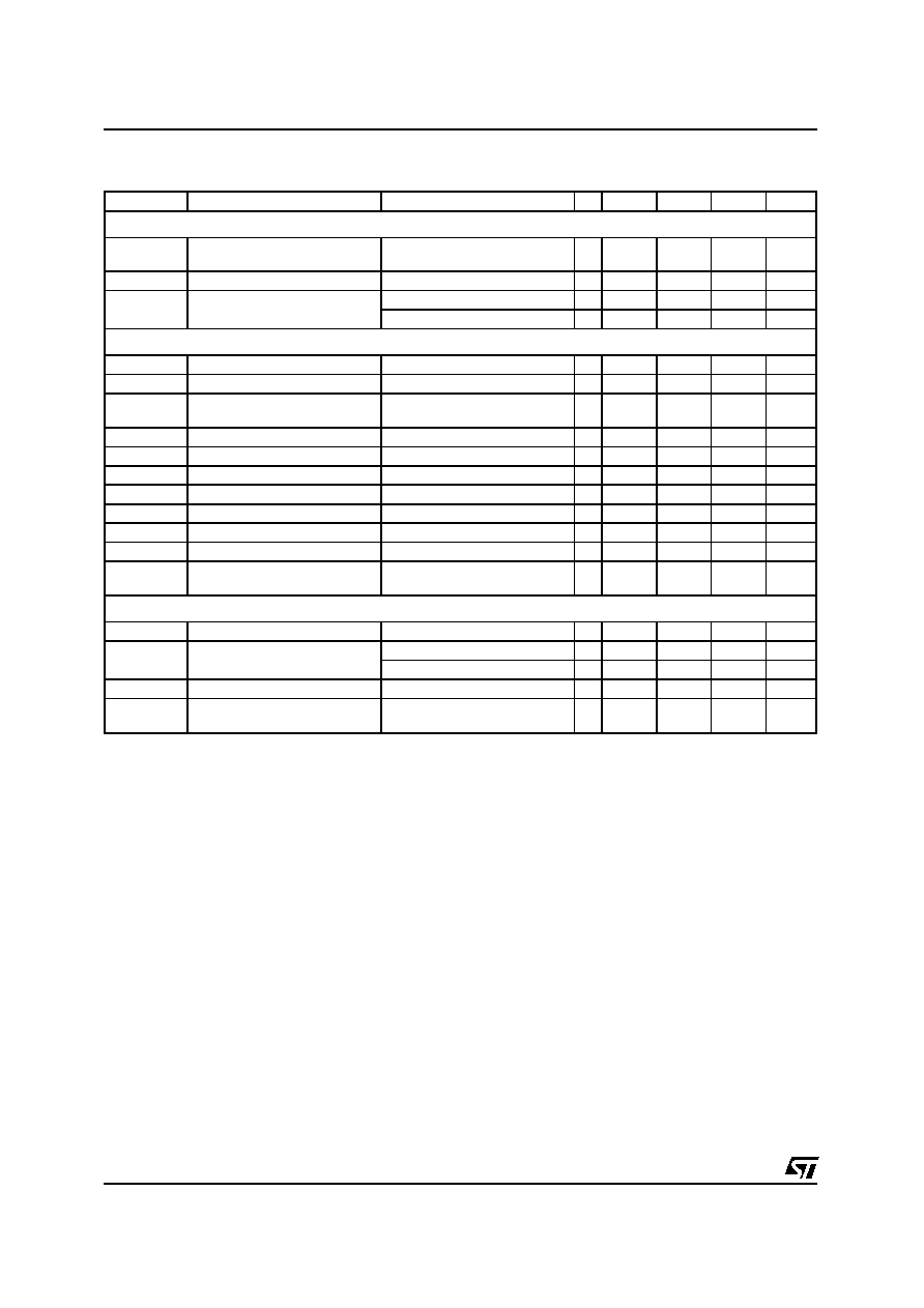
The device is available in plastic dual in line,
MINIDIP 8 for standard assembly, and SO16W
for SMD assembly.
October 2001
Æ
ORDERING NUMBERS: L4978 (Minidip)
L4978D (SO16)
L4978
2A STEP DOWN SWITCHING REGULATOR
Minidip
SO16W
D98IN837A
5
2
8
4
1
L4978
C
1
220
µ
F
63V
C
8
330
µ
F
V
O
=3.3V/2A
Vi=8V to 55V
R
1
20K
C
2
2.7nF
R
2
9.1K
C
4
22nF
3
7
L1
126
µ
H
(77120)
6
D1
GI
SB560
C
5
100nF
C
7
220nF
C
6
100nF
TYPICAL APPLICATION CIRCUIT
1/12
PIN FUNCTIONS
DIP
SO (*)
Name
Function
1
2
GND
Ground
2
3
SS_INH
A logic signal (active low) disables the device (sleep mode operation).
A capacitor connected between this pin and ground determines the soft start time.
When this pin is grounded disables the device (driven by open collector/drain).
3
4
OSC
An external resistor connected between the unregulated input voltage and this pin and
a capacitor connected from this pin to ground fix the switching frequency. (Line feed
forward is automatically obtained)
4
5, 6
OUT
Stepdown regulator output
5
11
V
CC
Unregulated DC input voltage
6
12
BOOT
A capacitor connected between this pin and OUT allows to drive the internal DMOS
Transistors
7
13
COMP
E/A output to be used for frequency compensation
8
14
FB
Stepdown feedback input. Connecting directly to this pin results in an output voltage of
3.3V. An external resistive divider is required for higher output voltages.
(*) Pins 1, 7, 8, 9, 10, 15 and 16 are not internally, electrically connected to the die.
PIN CONNECTIONS
GND
SS_INH
OSC
OUT
1
3
2
4
VCC
BOOT
COMP
FB
8
7
6
5
D97IN595
N.C.
GND
SS_INH
OSC
OUT
N.C.
OUT
N.C.
N.C.
N.C.
BOOT
VCC
COMP
FB
N.C.
N.C.
1
3
2
4
5
6
7
8
14
13
12
11
10
9
15
16
D97IN596
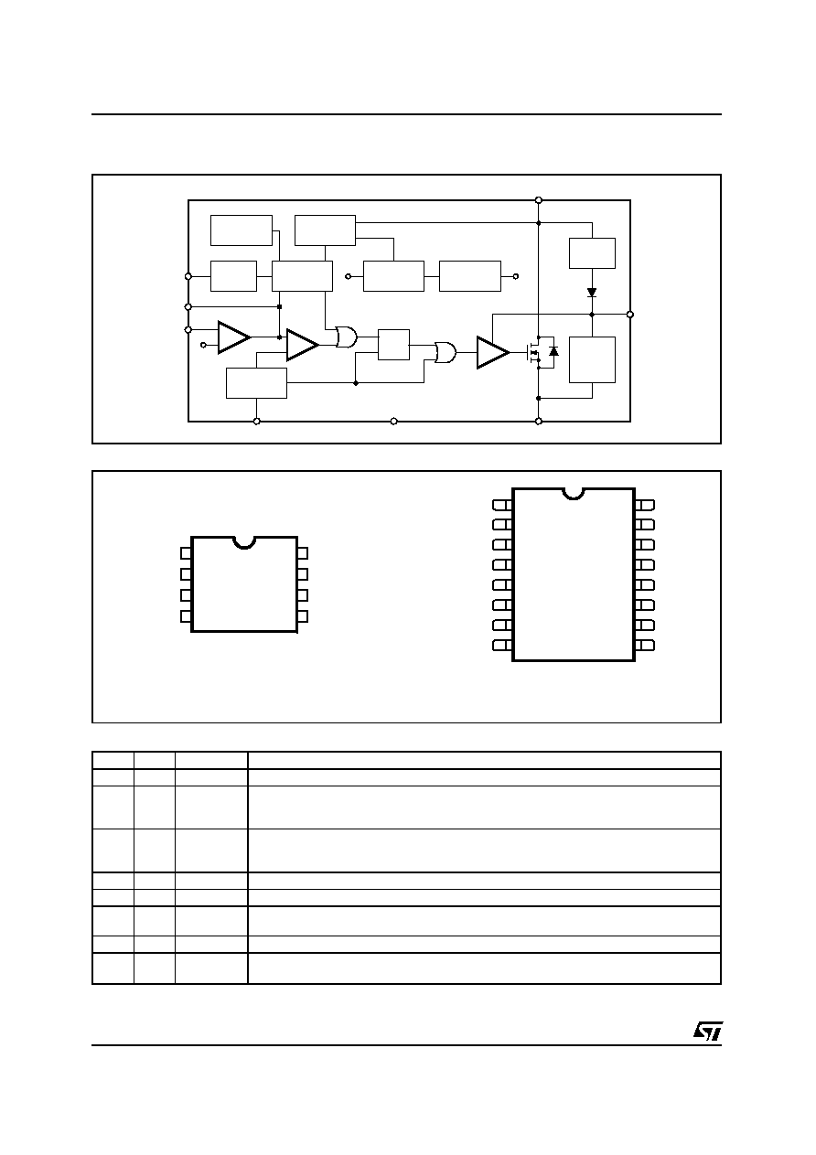
INHIBIT
SOFTSTART
VOLTAGES
MONITOR
THERMAL
SHUTDOWN
E/A
PWM
3.3V
OSCILLATOR
R
S
Q
INTERNAL
REFERENCE
INTERNAL
SUPPLY
3.3V
5.1V
DRIVE
CBOOT
CHARGE
CBOOT
CHARGE
AT LIGHT
LOADS
2
7
8
FB
COMP
SS_INH
3
1
4
6
5
BOOT
OSC
GND
OUT
VCC
D97IN594
BLOCK DIAGRAM
Minidip
SO16W
L4978
2/12

ELECTRICAL CHARACTERISTICS (T
j
= 25∞C, C
osc
= 2.7nF, Rosc = 20k
, V
CC
= 24V, unless other-
wise specified.) * Specification Refered to T
j
from 0 to 125∞C
Symbol
Parameter
Test Condition
Min.
Typ.
Max.
Unit
Dynamic Characteristic
V
I
Operating input voltage range
V
o
= 3.3 to 50V; I
o
= 2A
∑
8
55
V
V
o
Output voltage
I
o
= 0.5A
3.33
3.36
3.39
V
I
o
= 0.2 to 2A
3.292
3.36
3.427
V
V
cc
= 8 to 55V
∑
3.22
3.36
3.5
V
V
d
Dropout voltage
V
cc
= 10V; I
o
= 2A
0.58
0.733
V
∑
1.173
V
I
l
Maximum limiting current
V
cc
= 8 to 55V
∑
2.5
3
3.5
A
Efficiency
V
o
= 3.3V; I
o
= 2A
87
%
f
s
Switching frequency
∑
90
100
110
KHz
SVRR
Supply voltage ripple rejection
V
i
= V
cc
+2V
RMS
; V
o
= V
ref
;
I
o
= 2.5A; f
ripple
= 100Hz
60
dB
Switching Frequency Stability
vs. V
cc
Vcc = 8 to 55V
3
6
%
Temp. stability of switching
frequency
T
j
= 0 to 125∞C
4
%
Soft Start
Soft start charge current
30
40
50
µ
A
Soft start discharge current
6
10
14
µ
A
Inhibit
V
LL
Low level voltage
∑
0.9
V
I
sLL
Isource Low level
∑
5
15
µ
A
THERMAL DATA
Symbol
Parameter
Minidip
SO16
Unit
R
th(j-amb)
Thermal Resistance Junction to ambient Max.
90 (*)
110 (*)
∞C/W
(*) Package mounted on board.
ABSOLUTE MAXIMUM RATINGS
Symbol
Parameter
Value
Unit
Minidip
S016
V
5
V
11
Input voltage
58
V
V
4
V
5
,V
6
Output DC voltage
Output peak voltage at t = 0.1
µ
s f=200KHz
-1
-5
V
V
I
4
I
5
,I
6
Maximum output current
int. limit.
V
6
-V
5
V12-V
11
14
V
V
6
V
12
Bootstrap voltage
70
V
V
7
V
13
Analogs input voltage (V
CC
= 24V)
12
V
V
2
V3
Analogs input voltage (V
CC
= 24V)
13
V
V
8
V
14
(V
CC
= 20V)
6
-0.3
V
V
P
tot
Power dissipation a T
amb
60
∞
C
Minidip
1
W
SO16
0.8
W
T
j
,T
stg
Junction and storage temperature
-40 to 150
∞
C
L4978
3/12
Symbol
Parameter
Test Condition
Min.
Typ.
Max.
Unit
DC Characteristics
I
qop
Total operating quiescent
current
4
6
mA
I
q
Quiescent current
Duty Cycle = 0; V
FB
= 3.8V
2.5
3.5
mA
I
qst-by
Total stand-by quiescent
current
V
inh
<0.9V
100
200
µ
A
Vcc = 55V; V
inh
<0.9V
150
300
µ
A
Error Amplifier
V
FB
Voltage Feedback Input
3.33
3.36
3.39
V
R
L
Line regulation
Vcc = 8 to 55V
5
10
mV
Ref. voltage stability vs
temperature
∑
0.4
mV/∞C
V
oH
High level output voltage
V
FB
= 2.5V
10.3
V
V
oL
Low level output voltage
V
FB
= 3.8V
0.65
V
I
o source
Source output current
V
comp
= 6V; V
FB
= 2.5V
180
220
µ
A
I
o sink
Sink output current
V
comp
= 6V; V
FB
= 3.8V
200
300
µ
A
I
b
Source bias current
2
3
µ
A
SVRR E/A
Supply voltage ripple rejection
V
comp
= V
fb
; Vcc = 8 to 55V
60
80
dB
DC open loop gain
R
L
=
50
57
dB
gm
Transconductance
I
comp
= -0.1 to 0.1mA
V
comp
= 6V
2.5
mS
Oscillator Section
Ramp Valley
0.78
0.85
0.92
V
Ramp peak
Vcc = 8V
2
2.15
2.3
V
Vcc = 55V
9
9.6
10.2
V
Maximum duty cycle
95
97
%
Maximum Frequency
Duty Cycle = 0%
R
osc
= 13k
, C
osc
= 820pF
300
kHz
ELECTRICAL CHARACTERISTICS (continued)
L4978
4/12
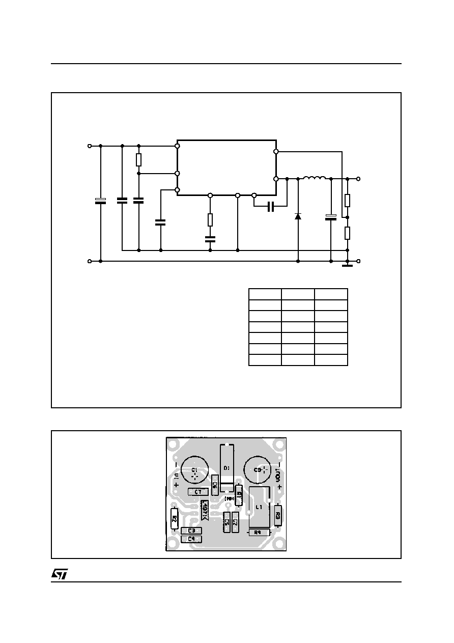
D98IN834A
5
2
8
4
1
L4978
C
1
220
µ
F
63V
C
8
330
µ
F
V
O
=3.3V/2A
Vi=8V to 55V
R
1
20K
C
2
2.7nF
R
2
9.1K
C
4
22nF
3
7
L1
126
µ
H
(77120)
6
D1
GI
SB560
C
5
100nF
C
7
220nF
C
6
100nF
R
3
R
4
C1=220
µ
F/63V EKE
C2=2.7nF
C5=100nF
C6=100nF
C7=220nF/63V
C8=330
µ
F/35V CG Sanyo
L1=126
µ
H KoolMu 77120 - 55 Turns - 0.5mm
R1=20K
R2=9.1K
D1=GI SB560
V
O
(V)
R3(K
)
R4(K
)
3.3
5.1
12
15
18
24
0
2.7
12
16
20
30
4.7
4.7
4.7
4.7
4.7
L4978
Figure 1. Test and evaluation board circuit.
Figure 2. PCB and component layout of the figure 1.
L4978
5/12
0
5 10 15 20 25 30 35 40 45 50
Vcc(V)
1
2
3
4
5
Iq
(mA)
200KHz
R
1
=22K
C
2
=1.2nF
0Hz
D97IN724
Tamb=25∞C
0% DC
100KHz
R
1
=20K
C
2
=2.7nF
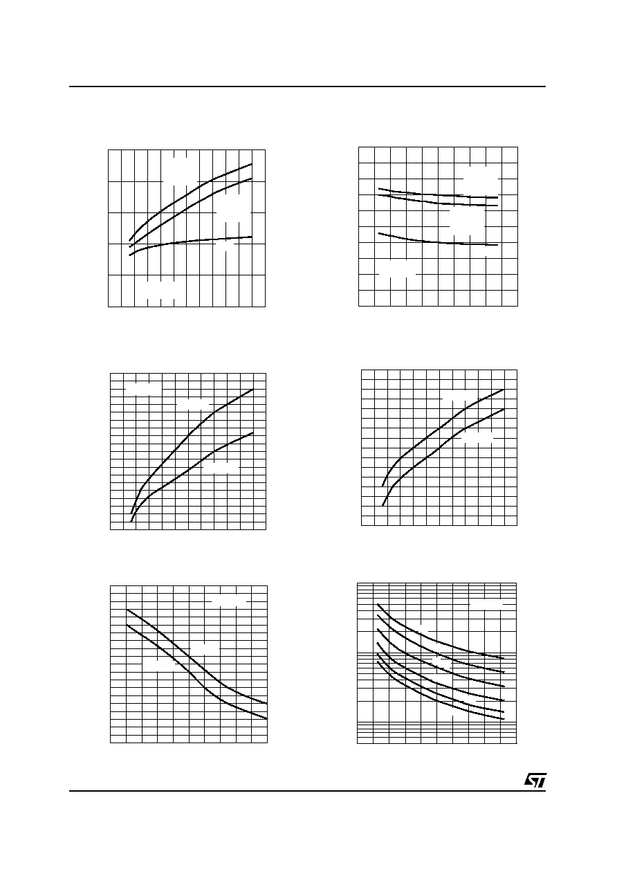
Figure 3. Quiescent drain current vs. input
voltage.
0
0.2 0.4 0.6
1.0 1.2 1.4 1.6
I
O
(A)
0.8
1.8
3.360
3.362
3.364
3.366
3.368
3.370
3.372
3.374
3.376
3.378
V
O
(V)
Tj=25∞C
Tj=125∞C
V
CC
=35V
D98IN835
Figure 7. Load regulation
0
5 10 15 20 25 30 35 40 45 50 V
CC
(V)
60
70
80
90
100
110
120
130
140
150
Ibias
(
µ
A)
D97IN732
Tj=25∞C
Tj=125∞C
Vss=GND
Figure 5. Stand by drain current vs. input
voltage
-50 -30 -10 10 30 50 70 90 110
Tj(∞C)
1
2
3
4
5
Iq
(mA)
D97IN731
0Hz
200KHz
R
1
=22K
C
2
=1.2nF
V
CC
=35V
0% DC
100KHz
R
1
=20K
C
2
=2.7nF
Figure 4. Quiescent current vs. junction
temperature
0
20
40
60
80
R1(K
)
5
10
20
50
100
200
500
fsw
(KHz)
D97IN784
0.82nF
1.2nF
2.2nF
3.3nF
4.7nF
5.6nF
Tamb=25∞C
Figure 8. Switching frquency vs. R1 and C2
0
5 10 15 20 25 30 35 40 45 50 V
CC
(V)
3.370
3.371
3.372
3.373
3.374
3.375
3.376
3.377
V
O
(V)
D97IN733
Tj=25∞C
Tj=125∞C
Figure 6. Line Regulation
L4978
6/12
0
5 10 15 20 25 30 35 40 45 50 V
CC
(V)
90.0
92.5
95.0
97.5
100.0
102.5
105.0
107.5
fsw
(KHz)
D97IN735
Tj=25∞C
Figure 9. Switching Frequency vs. input
voltage.
0
0.2 0.4 0.6 0.8
1
1.2 1.4 1.6 1.8
2
2.2
60
65
70
75
80
85
90
95
Io [A]
[%]
Vcc=8V
Vcc=12V
Vcc=24V
Vcc=48V
Vo=3.36V
fsw=100kHz
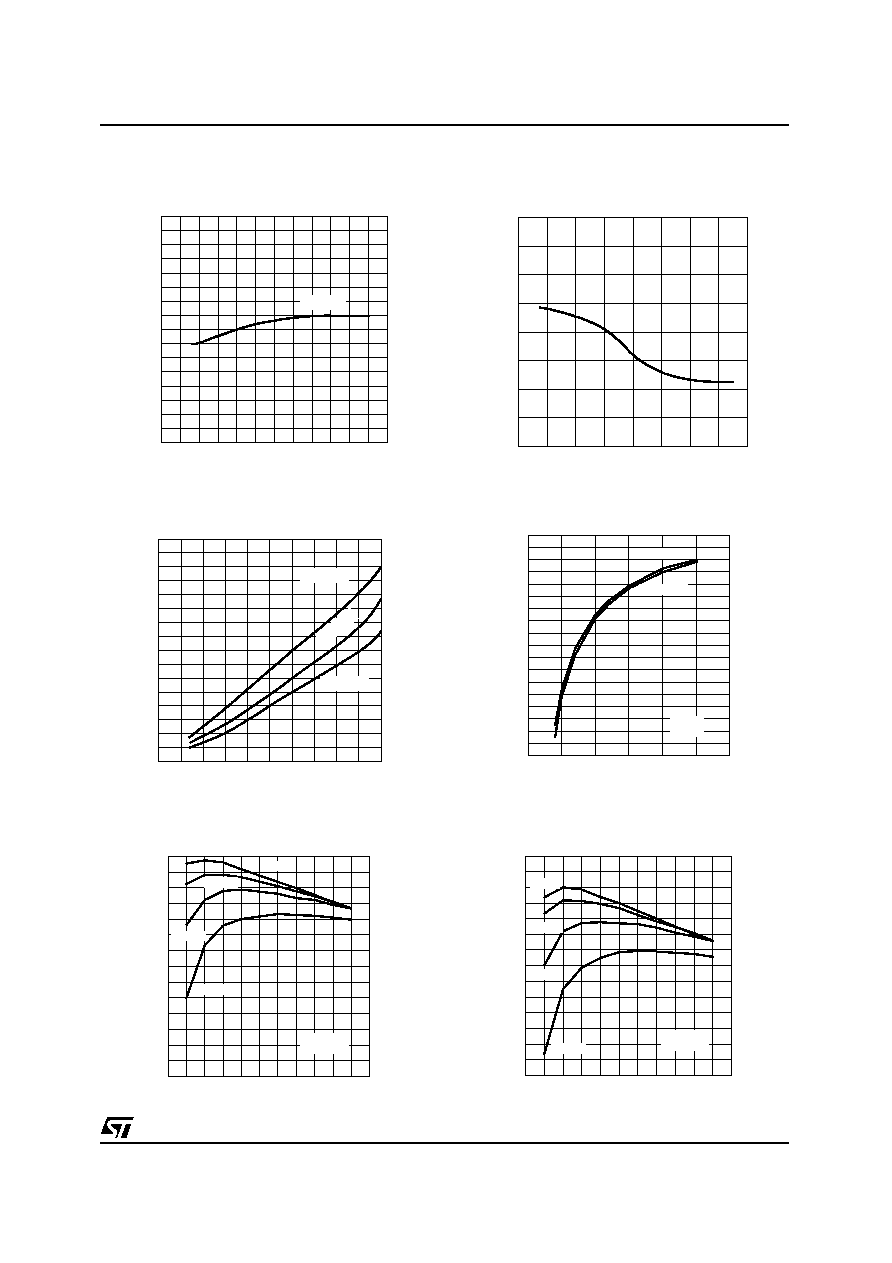
Figure 14. Efficiency vs. output current.
0
5
10
15
20
25
30
80
82
84
86
88
90
92
94
96
98
Vo [V]
[%]
fsw=100kHz
fsw=200kHz
Vcc=35V
Io=2A
Figure 12. Efficiency vs output voltage.
0.0 0.2 0.4 0.6 0.8 1.0 1.2 1.4
I
O
(A)
1.6 1.8
0.0
0.1
0.2
0.3
0.4
0.5
V
(V)
0.6
0.7
Tj=25∞C
Tj=125∞C
D98IN836
Tj=-25∞C
Figure 11. Dropout voltage between pin 5
and 4.
Vcc=12V
Vcc=8V
0
0.2 0.4 0.6 0.8
1
1.2 1.4 1.6 1.8
2
2.2
60
65
70
75
80
85
90
95
Io [A]
[%]
Vcc=8V
Vcc=12V
Vcc=24V
Vcc=48V
fsw=100kHz
Vo=5.1V
Figure 13. Efficiency vs. output current.
-50
0
50
100
Tj(∞C)
90
95
100
105
fsw
(KHz)
D97IN785
Figure 10. Switching frequency vs. junction
temperature.
L4978
7/12

0
0.2
0.4
0.6
0.8
1.0
1.2
1.4 I
O
(A)
60
65
70
75
80
85
90
(%)
D97IN740
V
CC
=8V
fsw=200KHz
V
O
=5.1V
V
CC
=12V
V
CC
=24V
V
CC
=48V
Figure 15. Efficiency vs. output current.
0.0
0.2
0.4
0.6
0.8
1.0
1.2
1.4 I
O
(A)
55
60
65
70
75
80
85
90
(%)
D97IN741
V
CC
=8V
fsw=200KHz
V
O
=3.36V
V
CC
=12V
V
CC
=24V
V
CC
=48V
Figure 16. Efficiency vs. output current.
Io=2A
0
10
20
30
40
50
60
70
75
80
85
90
Vcc [V]
n [%]
Vo=5.1V fsw=100kHz
Vo=5.1V fsw=200kHz
Vo=3.36V fsw=100kHz
Vo=3.36V fsw=200kHz
Figure 17. Efficiency vs. Vcc.
Io=0.5A
Io=2A
Io=1A
0
10
20
30
40
50
60
0
200
400
600
800
1000
Vcc [V]
Pdiss [mW]
Io=1.5A
Vo=5.1V
fsw=100kHz
Figure 18. Power dissipation vs. Vcc.
Io=2A
Io=1A
0
10
20
30
0
200
400
600
800
1000
1200
1400
Vo [V]
Pdiss [mW]
Io=0.5A
Io=1.5A
Vcc=35V
fsw=100kHz
Figure 19. Device Power dissipation vs. Vo
-50 -25
0
25
50
75
100 125 Tj(∞C)
2.3
2.4
2.5
2.6
2.7
2.8
2.9
Ilim
(A)
D97IN747
fsw=100KHz
V
CC
=35V
Figure 20. Pulse by pulse limiting current vs.
junction temperature.
L4978
8/12

Figure 21. Load transient.
10
10
3
10
5
10
7
f(Hz)
10
2
10
4
10
6
10
8
-200
-150
-100
-50
GAIN
(dB)
0
50
Phase
0
45
90
135
D97IN787
GAIN
Phase
Figure 25. Open loop frequency and phase of er-
ror amplifier
15
20
25
30
35
40
45
50 V
CCmax
(V)
0
100
200
300
400
L
(
µ
H)
D97IN745
680nF
fsw=100KHz
470nF
330nF
220nF
100nF
Figure 23. Soft start capacitor selection Vs in-
ductor and Vccmax.
2
1
D97IN786
V
CC
(V)
30
20
10
V
O
(mV)
100
0
-100
1ms/DIV
I
O
= 1A
f
sw
= 100KHz
Figure 22. Line transient.
15
20
25
30
35
40
45
50 V
CC
max(V)
0
100
200
300
L
(
µ
H)
56nF
fsw=200KHz
D97IN746
47nF
33nF
22nF
Figure 24. Soft start capacitor selection vs. In-
ductor and Vccmax.
L4978
9/12

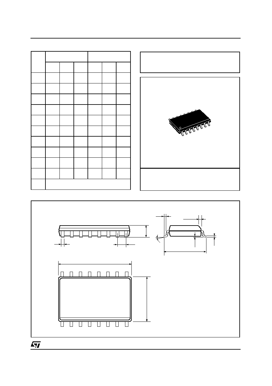
OUTLINE AND
MECHANICAL DATA
DIM.
mm
inch
MIN.
TYP.
MAX.
MIN.
TYP.
MAX.
A
3.32
0.131
a1
0.51
0.020
B
1.15
1.65
0.045
0.065
b
0.356
0.55
0.014
0.022
b1
0.204
0.304
0.008
0.012
D
10.92
0.430
E
7.95
9.75
0.313
0.384
e
2.54
0.100
e3
7.62
0.300
e4
7.62
0.300
F
6.6
0.260
I
5.08
0.200
L
3.18
3.81
0.125
0.150
Z
1.52
0.060
Minidip
L4978
10/12
DIM.
mm
inch
MIN.
TYP.
MAX.
MIN.
TYP.
MAX.
A
2.35
2.65
0.093
0.104
A1
0.1
0.3
0.004
0.012
B
0.33
0.51
0.013
0.020
C
0.23
0.32
0.009
0.013
D
10.1
10.5
0.398
0.413
E
7.4
7.6
0.291
0.299
e
1.27
0.050
H
10
10.65
0.394
0.419
h
0.25
0.75
0.010
0.030
L
0.4
1.27
0.016
0.050
K
0∞ (min.)8∞ (max.)
h x 45
A
e
B
D
E
A1
H
L
C
K
16
1
8
9
SO16 Wide
OUTLINE AND
MECHANICAL DATA
L4978
11/12

Information furnished is believed to be accurate and reliable. However, STMicroelectronics assumes no responsibility for the consequences
of use of such information nor for any infringement of patents or other rights of third parties which may result from its use. No license is
granted by implication or otherwise under any patent or patent rights of STMicroelectronics. Specification mentioned in this publication are
subject to change without notice. This publication supersedes and replaces all information previously supplied. STMicroelectronics products
are not authorized for use as critical components in life support devices or systems without express written approval of STMicroelectronics.
The ST logo is a registered trademark of STMicroelectronics
© 2001 STMicroelectronics ≠ Printed in Italy ≠ All Rights Reserved
STMicroelectronics GROUP OF COMPANIES
Australia - Brazil - China - Finland - France - Germany - Hong Kong - India - Italy - Japan - Malaysia - Malta - Morocco -
Singapore - Spain - Sweden - Switzerland - United Kingdom - U.S.A.
http://www.st.com
L4978
12/12