 | –≠–ª–µ–∫—Ç—Ä–æ–Ω–Ω—ã–π –∫–æ–º–ø–æ–Ω–µ–Ω—Ç: L4979 | –°–∫–∞—á–∞—Ç—å:  PDF PDF  ZIP ZIP |

1/10
L4979D
L4979MD
February 2002
This is preliminary information on a new product now in development. Details are subject to change without notice.
s
OPERATING DC SUPPLY VOLTAGE RANGE
6V TO 31V
s
TRANSIENT SUPPLY VOLTAGE UP TO 40V
s
LOW QUIESCENT CURRENT CONSUMPTION
LESS THAN 20
µ
A WITH ENABLE LOW
s
HIGH PRECISION OUTPUT VOLTAGE (2%)
s
LOW DROPOUT VOLTAGE LESS THAN 0.5V
s
RESET CIRCUIT SENSING THE OUTPUT
VOLTAGE DOWN TO 1V
s
PROGRAMMABLE RESET PULSE DELAY
WITH EXTERNAL CAPACITOR
s
WATCHDOG
s
PROGRAMMABLE WATCHDOG TIMER WITH
EXTERNAL CAPACITOR
s
THERMAL SHUTDOWN AND SHORT
CIRCUIT PROTECTION
s
WIDE TEMPERATURE RANGE (T
j
= -40∞C TO
150∞C)
DESCRIPTION
L4979 is a family of low dropout linear regulators with
microprocessor control functions such as power on re-
set, low voltage reset, watchdog timer, on-off control or
Enable. In addition, only low value ceramic capacitor is
required for stability (above or equal to 100nF).
Maximum quiescent current is 20
µ
A at all output current
equal 0 and enable low.
Typical quiescent current is 1.5mA at output current
equal to 5mA, 3mA at output current equal to 150mA,
and drops to 10mA in "not enabled" mode.
On chip trimming results in high output voltage accu-
racy (2%). Accuracy is kept over wide temperature
range, line variation, load variation.
The maximum input voltage is 40V. The maximum
output current is 200mA. Output current is internally
limited. Internal temperature protection disables volt-
age regulator at overtemperature.
SO8
SO20
ORDERING NUMBERS:
L4979D
L4979MD
PRODUCT PREVIEW
LOW DROP VOLTAGE REGULATOR
BLOCK DIAGRAM
voltage reference
reset
watchdog
Vs
Vi
Wi
Vcw
Vcr
Ctr
Ctw
Res
En
gnd
Vo
Co
5V/3.3V, 150 mA

L4979MD L4979D
2/10
PIN FUNCTION
PINS CONNECTION
SO8
N∞
SO20
N∞
Pin
Name
Function
1
1
En
Voltage regulator enable
2
4, 5, 6,
15, 16
gnd
ground
3
7
Res
Reset output
4
10
Vcr
Reset timing adjust
5
11
Vcw
Watchdog timer adjust
6
14
Wi
Watchdog input
7
17
Vo
Voltage regulator output
8
20
Vs
Supply voltage
2, 3, 8,
9, 12,
13, 18,
19
N. C.
not connected
EN
GND
RES
VCR
VCW
WI
V
O
V
S
1
3
2
4
6
5
7
8
SO8
EN
N.C.
N.C.
GND
GND
RES
GND
N.C.
N.C.
N.C.
N.C.
WI
GND
GND
V
O
N.C.
N.C.
V
S
1
3
2
4
5
6
7
8
9
18
17
16
15
14
12
13
11
19
10
20
VCR
WCW
D00AT457
SO8
SO20

3/10
L4979MD L4979D
ABSOLUTE MAXIMUM RATINGS
Stresses above those listed under "Absolute Maximum Ratings" may cause permanent damage to the device. This is a stress rating only and
functional operation of the device at any condition above those indicated in the operational section of this specification is not implied.
Exposure to absolute maximum rating conditions for extended periods may affect device reliability.
THERMAL DATA
(*) with 6 sq. cm on board heat sink
ELECTRICAL CHARACTERISTCS
(V
s
= 5.6V to 31V, T
j
= -40∞C to +150∞C unless otherwise specified)
Symbol
Parameter
Value
Unit
Vvsdc
DC operating supply voltage
31
V
Vvstr
Transient operating supply voltage (t<400ms)
-0.3 to 40
V
Ivsdc
Input current
internally limited
Vvo
DC output voltage
-0.3 to 5.5
V
Ivo
DC output current
internally limited
Vwi
Watchdog input voltage
-0.3 to 7
V
Vod
Open drain output voltage (RES)
-0.3 to 7
V
Iod
Open drain output current (RES)
internally limited
Vcr
Reset delay voltage
-0.3 to 7
V
Vcw
Watchdog delay voltage
-0.3 to 7
V
Ven
Enable input voltage
-0.3 to 40
V
Tj
Junction temperature
-40 to 150
C
VESD
ESD voltage level (HBM-MIL STD 883C)
+/- 2
kV
Symbol
Parameter
Value
Unit
R
th j-amb
Thermal resistance Junction to Ambient (SO8)
130-180
∞C/W
R
th j-amb
Thermal resistance Junction to Ambient (SO12+4+4)
50 (*)
∞C/W
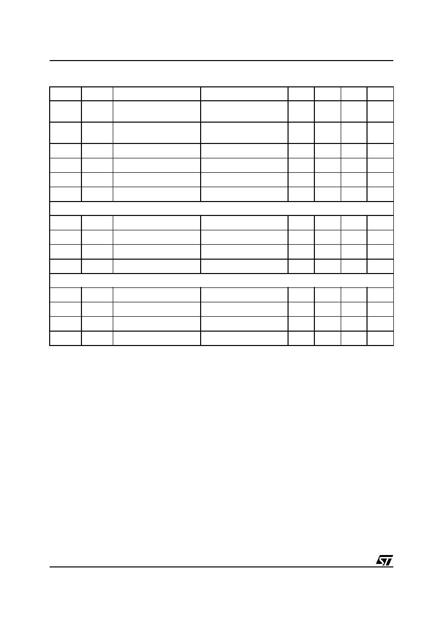
Pin
Symbol
Parameter
Test Condition
Min.
Typ.
Max.
Unit
GENERAL
V
s
, V
o
I
q
Quiescent current
V
s
= 13.5V, I
o
=150mA,
enable high
all I/O currents=0
3
6
mA
V
s
, V
o
I
q
Quiescent current
V
s
= 13.5V, I
o
= 0mA,
enable high
all I/O currents = 0
1.5
3
mA
V
s
, V
o
I
q
Quiescent current
V
s
= 13.5V, I
o
= 0mA,
enable low
all I/O currents = 0
20
µ
A
T
w
Thermal protection
temperature
150
190
∞C
T
w_hy
Thermal protection
temperature hysteresis
10
∞C

L4979MD L4979D
4/10
5V VOLTAGE REGULATOR
V
o
V
o_ref
Output voltage
V
s
= 5.6 to 31V
I
o
= 1 to 150mA
4.90
5.00
5.10
V
V
o
I
lim
Output current limitation
V
s
= 13.5V
200
300
400
mA
V
s
, V
o
V
line
Line regulation voltage
V
s
= 5.6 to 31V
I
o
= 1 to 150mA
25
mV
V
o
V
load
Load regulation voltage
I
o
= 1 to 150mA
25
mV
V
s
, V
o
V
dp
Drop voltage
I
o
= 150mA
300
500
mV
V
s
, V
o
SVR
Ripple rejection
f
r
= 100 Hz
55
dB
3.3V VOLTAGE REGULATOR
V
o
V
o_ref
Output voltage
V
s
= 5.6 to 31V
I
o
= 1 to 150mA
3.23
3.30
3.37
V
V
o
I
lim
Output current limitation
V
s
= 13.5V
200
300
400
mA
V
s
, V
o
V
line
Line regulation voltage
V
s
= 5.6 to 31V
I
o
= 1 to 150mA
25
mV
V
s
, V
o
V
dp
Drop voltage
I
o
= 150mA
500
1000
mV
V
o
V
load
Load regulation voltage
I
o
= 1 to 150mA
25
mV
V
s
, V
o
SVR
Ripple rejection
f
r
= 100 Hz
55
dB
RESET (5V)
R
es
V
res_l
Reset output low voltage
R
ext
= 5k
to Vo,
Vo > 1V
0.4
V
R
es
I
res_h
Reset output high leakage
current
V
res
= 5V
1
µ
A
R
es
R
_p_u
Pull up internal resistance
with respect to V
o
15
30
50
k
R
es
V
o_th
V
o
out of regulation
threshold
V
s
= 5.6 to 31V
I
o
= 1 to 150mA
6%
below
V
o_ref
8%
below
V
o_ref
10%
below
V
o_ref
V
cr
V
rhth
Reset timing high threshold
V
s
= 13.5V
10%
V
o_ref
13%
V
o_ref
16%
V
o_ref
V
cr
V
rlth
Reset timing low threshold
V
s
= 13.5V
44%
V
o_ref
47%
V
o_ref
50%
V
o_ref
V
cr
I
cr
Charge current
V
s
= 13.5V
8
17.6
30
µ
A
V
cr
I
dr
Discharge current
V
s
= 13.5V
8
17.6
30
µ
A
R
es
t
rr
Reset reaction time
see fig. 2
4
10
30
µ
s
R
es
t
rd
Reset pulse delay
V
s
= 13.5V, C
tr
= 1nF
65
150
ms
Pin
Symbol
Parameter
Test Condition
Min.
Typ.
Max.
Unit
ELECTRICAL CHARACTERISTICS (continued)

5/10
L4979MD L4979D
RESET (3.3V)
R
es
V
res_l
Reset output low voltage
R
ext
= 5k
to V
o
,
V
o
> 1V
0.4
V
R
es
I
res_h
Reset output high leakage
current
V
res
= 5V
1
µ
A
R
es
R
_p_u
Pull up internal resistance
with respect to V
o
15
30
50
k
R
es
V
o_th
Vo out of regulation
threshold
V
s
= 5.6 to 31V
I
o
= 1 to 150mA
6%
below
V
o_ref
8%
below
V
o_ref
10%
below
V
o_ref
V
cr
V
rhth
Reset timing high threshold
V
s
= 13.5V
10%
V
o_ref
13%
V
o_ref
16%
V
o_ref
V
cr
V
rlth
Reset timing low threshold
V
s
= 13.5V
44%
V
o_ref
47%
V
o_ref
50%
V
o_ref
V
cr
I
cr
Charge current
V
s
= 13.5V
8
17.6
30
µ
A
V
cr
I
dr
Discharge current
V
s
= 13.5V
8
17.6
30
µ
A
R
es
t
rr
Reset reaction time
see fig. 2
3
7.5
20
µ
s
R
es
t
rd
Reset pulse delay
V
s
= 13.5V, C
tr
= 1nF
40
65
100
ms
WATCHDOG (5V)
W
i
V
ih
Input high voltage
V
s
= 13.5V
3.5
V
W
i
V
il
Input low voltage
V
s
= 13.5V
1.5
V
W
i
V
ih
Input hysteresis
V
s
= 13.5V
100
mV
W
i
I
i
Pull down current
V
s
= 13.5V
10
µ
A
V
cw
V
whth
High threshold
V
s
= 13.5V
2.20
2.35
2.50
V
V
cw
V
wlth
Low threshold
V
s
= 13.5V
0.50
0.65
0.80
V
V
cw
I
cwc
Charge current
V
s
= 13.5V, V
cw
= 0.1V
4
8
14
µ
A
V
cw
I
cwd
Discharge current
V
s
= 13.5V, V
cw
= 2.5V
1.0
2.13
4.5
µ
A
V
cw
T
wop
Watchdog period
V
s
= 13.5V, C
tw
= 47nF
20
48
80
ms
R
es
t
wol
Watchdog output low time
V
s
= 13.5V, C
tw
= 47nF
5
10
18
ms
WATCHDOG (3.3V)
W
i
V
ih
Input high voltage
V
s
= 13.5V
2.3
V
W
i
V
il
Input low voltage
V
s
= 13.5V
1
V
W
i
V
ih
Input hysteresis
V
s
= 13.5V
50
mV
W
i
I
i
Pull down current
V
s
= 13.5V
10
µ
A
Pin
Symbol
Parameter
Test Condition
Min.
Typ.
Max.
Unit
ELECTRICAL CHARACTERISTICS (continued)
L4979MD L4979D
6/10
VOLTAGE REGULATOR
Voltage regulator uses a pchannel transistor as a regulating element. With this structure very low dropout volt-
age at current up to 150mA is obtained. The output voltage is regulated up to transient input supply voltage of
40V. No functional interruption due to over-voltage pulses is generated. The high precision of the output voltage
is obtained with a pre-trimmed reference voltage. A short circuit protection to GND is provided.
RESET
The reset circuit supervises the output voltage V
o
. The V
o_th
reset threshold is defined with the internal refer-
ence voltage and a resistor output divider. If the output voltage becomes lower than Vo_th then Res goes low
with a reaction time trr. If the output voltage becomes lower than 2.0V (typ) than Res goes immediately low. The
reset low signal is guaranteed for an output voltage V
o
greater than 1V.
When the output voltage becomes higher than V
o_th
then Res goes high with a delay t
rd
. This delay is obtained
by an internal oscillator. Oscillator period is given by
where:
I
cr
is an internally generated charge current,
V
cw
V
whth
Watchdog timing high
threshold
V
s
= 13.5V
1.45
1.55
1.65
V
V
cw
V
wlth
Watchdog timing low
threshold
V
s
= 13.5V
0.30
0.45
0.55
V
V
cw
I
cwc
Charge current
V
s
= 13.5V, V
cw
= 0.1V
4
8
14
µ
A
V
cw
I
cwd
Discharge current
V
s
= 13.5V, V
cw
= 2.5V
1.0
2.13
4.5
µ
A
V
cw
T
wop
Watchdog period
V
s
=13.5V, C
tw
= 47nF
13
32
54
ms
R
es
t
wol
Watchdog output low time
V
s
= 13.5V, C
tw
= 47nF
3.0
6.5
11.0
ms
ENABLE (5V)
E
n
V
en_l
Enable input low voltage
2.1
V
E
n
V
en_h
Enable input high voltage
3.4
V
E
n
V
en_hy
Enable input hysteresis
0.25
V
E
n
I
_leak
Pull down current
E
n
= 5V
5
20
40
µ
A
ENABLE (3.3V)
E
n
V
en_l
Enable input low voltage
2.0
V
E
n
V
en_h
Enable input high voltage
2.7
V
E
n
V
en_hy
Enable input hysteresis
0.2
V
E
n
I
_leak
Pull down current
E
n
= 5V
5
20
40
µ
A
Pin
Symbol
Parameter
Test Condition
Min.
Typ.
Max.
Unit
T
os c
V
rhth
V
rlth
≠
(
)
C
tr
[
]
I
c r
------------------------------------------------------
V
rhth
V
rlth
≠
(
)
C
tr
[
]
I
cd
------------------------------------------------------
+
=
ELECTRICAL CHARACTERISTICS (continued)

7/10
L4979MD L4979D
I
cd
is an internally generated discharge current,
V
rhth
and Vrlth are two voltages defined with the output voltage and a resistor output divider,
C
tr
is an external capacitance,
t
rd
is given by
t
rd
= 512 x T
osc
Figure 1. Reset Time Diagram.
WATCHDOG
A connected microcontroller is monitored by the watchdog input W
i
. If pulses are missing, the watchdog out-
put W
o
is set to low. The pulse sequence time can be set within a wide range with the external capacitor C
tw
.
The watchdog circuit discharges the capacitor C
tw
with the constant current I
cwd
. If the lower threshold V
wlth
is
reached, a watchdog reset is generated. To prevent this the microcontroller must generate a positive edge dur-
ing the discharge of the capacitor before the voltage has reached the threshold V
wlth
. In order to calculate the
minimum time t during which the microcontroller must output the positive edge the following equation can be
used:
(V
whth
- V
wlth
) x C
tw
= I
cwd
x t
Every W
i
positive edge switches the current source from discharging to charging, the same happens when the
lower threshold is reached. When the voltage reaches the upper threshold V
whth
the current switches from
charging to discharging. The result is a saw toothvoltage at the watchdog timer capacitor C
tw
.
Figure 2. Watchdog time diagram
trr
< trr
trd = 512 Tosc
Tosc
Vrhth
Vrlth
Res
Vcr
Vo
Wi
Vout_th
Res
Vcw
Wi
Vwlth
Vwhth
twol
Twop

L4979MD L4979D
8/10
DIM.
mm
inch
MIN.
TYP.
MAX.
MIN.
TYP.
MAX.
A
1.75
0.069
a1
0.1
0.25
0.004
0.010
a2
1.65
0.065
a3
0.65
0.85
0.026
0.033
b
0.35
0.48
0.014
0.019
b1
0.19
0.25
0.007
0.010
C
0.25
0.5
0.010
0.020
c1
45
∞
(typ.)
D (1)
4.8
5.0
0.189
0.197
E
5.8
6.2
0.228
0.244
e
1.27
0.050
e3
3.81
0.150
F (1)
3.8
4.0
0.15
0.157
L
0.4
1.27
0.016
0.050
M
0.6
0.024
S
8
∞
(max.)
(1) D and F do not include mold flash or protrusions. Mold flash or
potrusions shall not exceed 0.15mm (.006inch).
SO8
OUTLINE AND
MECHANICAL DATA

9/10
L4979MD L4979D
1
1
0
11
20
A
e
B
D
E
L
K
H
A1
C
SO20MEC
h x 45∞
SO20
DIM.
mm
inch
MIN.
TYP.
MAX.
MIN.
TYP.
MAX.
A
2.35
2.65
0.093
0.104
A1
0.1
0.3
0.004
0.012
B
0.33
0.51
0.013
0.020
C
0.23
0.32
0.009
0.013
D
12.6
13
0.496
0.512
E
7.4
7.6
0.291
0.299
e
1.27
0.050
H
10
10.65
0.394
0.419
h
0.25
0.75
0.010
0.030
L
0.4
1.27
0.016
0.050
K
0∞ (min.)8∞ (max.)
OUTLINE AND
MECHANICAL DATA

Information furnished is believed to be accurate and reliable. However, STMicroelectronics assumes no responsibility for the consequences
of use of such information nor for any infringement of patents or other rights of third parties which may result from its use. No license is granted
by implication or otherwise under any patent or patent rights of STMicroelectronics. Specifications mentioned in this publication are subject
to change without notice. This publication supersedes and replaces all information previously supplied. STMicroelectronics products are not
authorized for use as critical components in life support devices or systems without express written approval of STMicroelectronics.
The ST logo is a registered trademark of STMicroelectronics
Æ
2002 STMicroelectronics - All Rights Reserved
STMicroelectronics GROUP OF COMPANIES
Australia - Brazil - Canada - China - Finland - France - Germany - Hong Kong - India - Israel - Italy - Japan -Malaysia - Malta - Morocco -
Singapore - Spain - Sweden - Switzerland - United Kingdom - United States.
http://www.st.com
10/10
L4979MD - L4979D