 | –≠–ª–µ–∫—Ç—Ä–æ–Ω–Ω—ã–π –∫–æ–º–ø–æ–Ω–µ–Ω—Ç: L497B | –°–∫–∞—á–∞—Ç—å:  PDF PDF  ZIP ZIP |

L497
March 1998
HALL EFFECT PICKUP IGNITION CONTROLLER
.
DIRECT
DRIVING
OF
THE
EXTERNAL
POWER DARLINGTON
.
COIL CURRENT CHARGING ANGLE (dwell)
CONTROL
.
PROGRAMME COIL CURRENT PEAK LIMITA-
TION
.
PROGRAMMABLE DWELL RECOVERY TIME
WHEN 94 % NOMINAL CURRENT NOT
REACHED
.
RPM OUTPUT
.
PERMANENT CONDUCTION PROTECTION
.
OVERVOLTAGE PROTECTION FOR EXTER-
NAL DARLINGTON
.
INTERNAL SUPPLY ZENER
.
REVERSE BATTERY PROTECTION
DESCRIPTION
The L497 is an integratedelectronic ignition control-
ler for breakerless ignition systems using Hall effect
sensors.
ORDERING NUMBERS : L497B (DIP16)
L497D1 (SO16)
DIP16
SO16
The device drives an NPN external darlington to
control the coil current providingthe required stored
energy with low dissipation.
A special feature of the L497 is the programmable
time for the recovery of the correct dwell ratio T
d
/T
when the coil peak current fails to reach 94 % of the
nominal value. In this way only one spark may have
an energy less than 94 % of the nominal one during
fast acceleration or cold starts.
BLOCK DIAGRAM
1/11

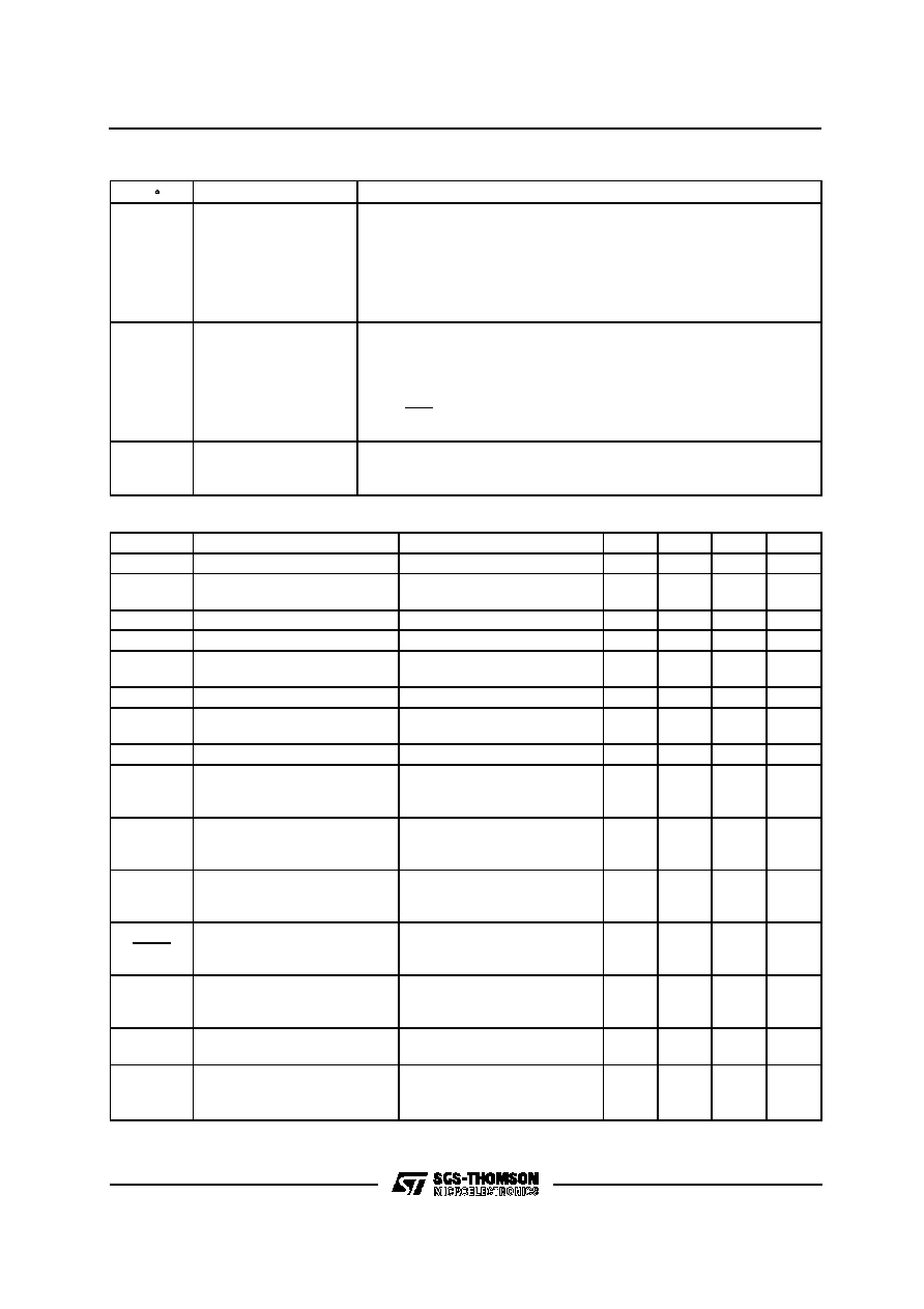
ABSOLUTE MAXIMUM RATINGS
Symbol
Parameter
Value
Unit
I
3
D.C. Supply current
Transient Supply Current (t
f
fall time constant = 100ms)
200
800
mA
mA
V
3
Supply Voltage
Int. Limited to Vz
3
V
6
RPM Voltage
28
V
I
16
D.C. Driver Collector Current
Pulse "
"(t <= 3ms)
300
600
mA
mA
V
16
Driver Collector Voltage
28
V
I
7
Auxiliary Zener Current
40
mA
I
15
D.C. Overvoltage Zener Current
Pulse "
" t
fall
= 300
µ
s,
tr
ep
Repetition Time > = 3ms
15
35
mA
mA
V
R
Reverse Battery Voltage if Application Circuit of Fig. 4 is used
≠ 16
V
T
j
, T
stg
Junction and StorageTemperature Range
≠ 55 to 150
∞
C
P
tot
Power Dissipation
at T
aluminia
= 90
∞
C for SO-16
T
amb
= 90
∞
C for DIP-16
1.2
0.65
W
W
PIN CONNECTION (top view)
THERMAL DATA
Symbol
Parameter
Value
Unit
R
th j-amb
R
th j-alumin
(*)
Thermal Resistance Junction-ambient for DIP-16
Thermal Resistance Junction-alumina for SO-16
Max
Max
90
50
∞
C/W
∞
C/W
(* ) Thermal resistance ju nction-aluminia wi th the device soldered on the mi ddle of an aluminia supporting substrate mesuri ng
15 x 20 ; 0.65 mm thickness.
L497
2/11

PIN FUNCTIONS (refer to fig. 4)
N
∞
Name
Function
1
GND
This pin must be connected to ground.
2
SIGNAL GND
This pin must be connected to ground.
3
POWER SUPPLY
Supply Voltage Input. An internal 7.5 V (typ) zener zener limits the voltage
at this pin. The external resistor R
5
limits the current through the zener for
high supply voltages.
4
N.C.
This pin must be connected to ground or left open.
5
HALL-EFFECT INPUT
Hall-effect Pickup Signal Input. This input is dwell control circuit output in
order to enable the current driving into the coil. The spark occurs at the
high-to-low transition of the hall-effect pickup signal.
Furthermore this input signal enables the slow recovery and permanent
conduction protection circuits. The input signal, supplied by the open
collector output stage of the Hall effect sensor, has a duty-cycle typically
about 70 %. V
5
is internally clamped to V
3
and ground by diodes
6
RPM OUTPUT
Open collector output which is at a low level when current flows in the
ignition coil. For high voltages protection of this output, connection to the
pin 7 zener is recommended.
In this situation R
8
must limit the zener current, too, and R
1
limits pin 6
current if RPM module pad is accidentally connected to V
S
.
7
AUX. ZENER
A 21 V (typ) General Purpose Zener. Its current must be limited by an
external resistor.
8
RECOVERY TIME
A capacitor connected between this pin and ground sets the slope of the
dwell time variation as it rises from zero to the correct value. This occurs
after the detection of I
coll
94 % I
nom
, just before the low transition of the
hall-effect signal pulse.
The duration of the slow recovery is given by :
t
src
= 12,9 R
7
C
src
(ms)
where R
7
is the biasing resistor at pin 12 (in K
) and C
src
is the delay
capacitor at pin 8 (in
µ
F).
9
MAX CONDUCTION
TIME
A capacitor connected between this pin and ground determines the
intervention delay of the permanent conduction protection. After this delay
time the coil current is slowly reduced to zero.
Delay Time T
p
is given by :
T
p
=16 C
p
R
7
(ms)
where R
7
is the biasing resistor at pin 12 (in K
) and C
P
is the delay
capacitor at pin 9 (in
µ
F).
10
DWELL CONTROL
TIMER
A capacitor C
T
connected between this pin and ground is charged when the
HAll effect output is High and is discharged at the High to Low transition of
the Hall effect signal.
The recommended value is 100 nF using a 62 K
resistor at pin 12.
11
DWELL CONTROL
The average voltage on the capacitor CW connected between this pin and
ground depends on the motor speed and the voltage supply. The
comparison between V
CW
and V
CT
voltage determines the timing for the
dwell control. For the optimized operation of the device C
T
= C
W
; the
recommended value is 100 nF using a 62 K
resistor at pin 12.
12
BIAS CURRENT
A resistor connected between this pin and ground sets the internal current
used to drive the external capacitors of the dwell control
(pin 10 and 11) permanent conduction protection (pin 9) and slow recovery
time (pin 8). The recommended value is 62 K
.
13
CURRENT SENSING
Connection for the Coil Current Limitation. The current is measured on the
sensing resitor R
S
and taken through the divider R
10
/R
11
. The current
limitation value is given by :
I
sens
=
0.32
R
10
+
R
11
R
S
R
11
L497
3/11
PIN FUNCTIONS (continued)
N
∞
Name
Function
14
DRIVER EMITT ER
OUTPUT
Current Driver for the External Darlington. To ensure stability and precision
of T
desat
C
c
and R
9
must be used. Recommended value for R
9
is 2 K
in
order not to change the open loop gain of the system.
R
c
may be added to C
c
to obtain greater flexibility in various application
situations.
C
c
and R
c
values ranges are 1 to 100 nF and 5 to 30 K
depending on the
external darlington type.
15
OVERVOLTAGE LIMIT
The darlington is protected against overvoltage by means of an internal
zener available at this pin and connected to pin 14. The internal divider
R
3
/R
2
defines the limitation value given by :
V
ovp
=
22.5
R
3
+
5.10
-
3
R
2
+
22.5
16
DRIVER COLLECTOR
INPUT
The collector current of the internal driver which drives the external
darlington is supplied through this pin. Then the external resistor R
6
limits
the maximum current supplied to the base of the external darlington.
ELECTRICAL CHARACTERISTICS (V
S
= 14.4 V, ≠ 40
∞
C < T
j
< 125
∞
C unless otherwise specified)
Symbol
Parameter
Test Conditions
Min.
Typ.
Max.
Unit
V
3
Min Op. Voltage
3.5
V
I
3
Supply Current
V
3
= 6 V
V
3
= 4 V
5
7
18
25
13
mA
mA
V
S
Voltage Supply
28
V
V
Z3
Supply Clamping Zener Voltage
I
Z3
= 70 mA
6.8
7.5
8.2
V
V
5
Input Voltage
Low Status
High Status
2.5
0.6
V
V
I
5
Input Current
V
5
= LOW
≠ 400
≠ 50
µ
A
V
16≠14
Darlington Driver Sat. Current
I
14
= 50 mA
I
14
= 180 mA
0.5
0.9
V
V
V
SENS
Current Limit. Sensing Voltage
V
S
= 6 to 16 V
260
320
370
mV
I
11C
C
W
Charge Current
V
S
= 5.3 to 16V
V
11
= 0.5V
T = 10 to 33ms
≠ 11.0
≠ 9.3
≠ 7.8
µ
A
I
11D
CW Charge Current
V
S
= 5.3 to 16V
V
11
= 0.5V
T = 10 to 33ms
0.5
0.7
1.0
µ
A
I
11C
/ I
11D
VS = 5.3 to 16V
V
11
= 0.5V
T = 10 to 33ms
See Note 1
7.8
22.0
I
SRC
I
SENSE
Percentage of Output Current
Determining the Slow Recovery
Control Start (fig. 2), note 1
90
94
98.5
%
T
SRC
Duration of Altered Small Contr.
Ratio after SRC Function Start
(fig. 2)
C
SRC
= 1
µ
F
R
7
= 62 K
0.8
s
V
Z15
External Darlington over V Prot.
Zener Voltage
I
15
= 5 mA
I
15
= 2 mA
19
18
22.5
21.5
26
25
V
V
T
P
Permanent Conduction Time
V
5
= High
C
P
= 1
µ
F
R
7
= 62K
0.4
1.1
1.8
s
L497
4/11

ELECTRICAL CHARACTERISTICS (continued)
Symbol
Parameter
Test Conditions
Min.
Typ.
Max.
Unit
V
6SAT
RPM Output Saturation Voltage
I
6
= 18.5 mA
I
6
= 25 mA
0.5
0.8
V
V
I
6 leak
RPM Output Leakage Current
V
S
= 20 V
50
µ
A
V
Z7
Auxiliary Zener Voltage
I
7
= 20 mA
19
27
V
V
12
Reference Voltage
1.20
1.25
1.30
V
Figure 1 : Main Waveforms.
APPLICATION INFORMATION
N otes : 1.
2.
td/t desaturation ratio is given by:
td
T
=
1
1
+
I
11C
/
I
11D
I
sense
= I
coil
when the external Darlington is in the active region.
L497
5/11