
1/13
October 2003
s
VERY LOW DROPOUT VOLTAGE
(0.25V TYP.)
s
DROPOUT CONTROL FLAG
s
VERY LOW QUIESCENT CURRENT
s
(TYP. 90 mA IN OFF MODE, 500mA IN ON
MODE)
s
OUTPUT CURRENT UP TO 200 mA
s
LOGIC-CONTROLLED ELECTRONIC
SHUTDOWN
s
OUTPUT VOLTAGES OF 3V, 3.3V, 5V, 8.7V,
12V
s
INTERNAL CURRENT AND THERMAL LIMIT
s
ONLY 2.2µF FOR STABILITY
s
AVAILABLE IN ± 2% SELECTION AT 25∞C
s
SUPPLY VOLTAGE REJECTION: 70dB (TYP.)
DESCRIPTION
The L4987 is a very low drop regulator available in
PPAK. The very low drop-voltage (0.5V Max at
200 mA) and the very low quiescent current make
it particularly suitable for low noise, low power
applications, and in battery powered systems. The
input dump protection up to 40V makes it ideal for
automotive
applications.
a
shutdown
Logic
Control
function
is
available
(pin2,
TTL
compatible). This means that when the device is
used as a local regulator, it is possible to put a part
of the board in standby, decreasing the total
power consumption. The regulator employs an
output pin (open collector) providing a logic signal
when the pass transistor is in saturation at low
input voltage, this signal can be used to prevent
the pop-up phenomenon in the car radio. In
battery powered systems (the cellular phone,
notebook) it is possible to use the flag to monitor
the battery charge status through the dropout of
the regulator.
L4987
SERIES
VERY LOW DROP VOLTAGE REGULATORS
WITH INHIBIT AND DROPOUT CONTROL FLAG
SCHEMATIC DIAGRAM
PPAK

L4987 SERIES
2/13
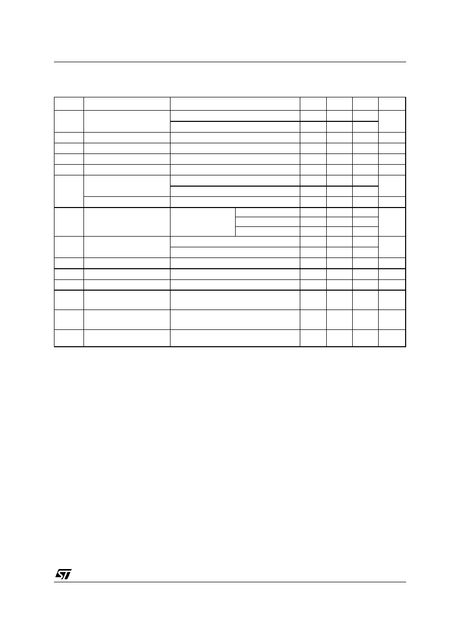
ABSOLUTE MAXIMUM RATINGS
Absolute Maximum Ratings are those values beyond which damage to the device may occur. Functional operation under these condition is
not implied.
THERMAL DATA
CONNECTION DIAGRAM (top view)
ORDERING CODES
(*) Available even in tape & reel.
Symbol
Parameter≤
Value
Unit
V
I
DC Input Voltage
40
V
I
O
Output Current
Internally Limited
P
tot
Power Dissipation
Internally Limited
T
stg
Storage Temperature Range
-40 to 150
∞C
T
op
Operating Junction Temperature Range
-40 to 125
∞C
Symbol
Parameter
PPAK
Unit
R
thj-case
Thermal Resistance Junction-case
8
∞C/W
R
thj-amb
Thermal Resistance Junction-ambient
100
∞C/W
TYPE
OUTPUT VOLTAGE
L4987CPT30 (*)
3.0 V
L4987CPT33 (*)
3.3 V
L4987CPT50 (*)
5.0 V
L4987CPT87 (*)
8.7 V
L4987CPT120 (*)
12 V

L4987 SERIES
3/13
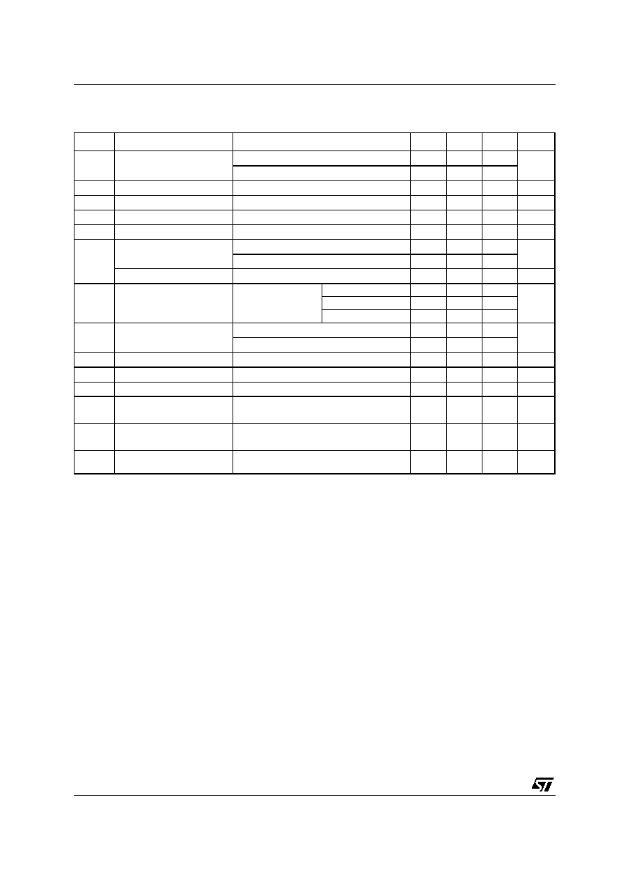
ELECTRICAL CHARACTERISTICS OF L4987CPT30 (refer to the test circuits, V
I
= 6V, I
O
= 5mA,
T
J
= 25∞C, C
I
= 0.1 µF, C
O
= 2.2 µF unless otherwise specified)
Symbol
Parameter
Test Conditions
Min.
Typ.
Max.
Unit
V
O
Output Voltage
I
O
= 200 mA V
I
= 6 V
2.94
3
3.06
V
I
O
= 200 mA V
I
= 6V
T
J
=-40 to 125∞C
2.88
3.12
V
I
Operating Input Voltage
I
O
= 200 mA
3.62
18
V
I
out
Output Current Limit
250
A
V
O
Line Regulation
V
I
= 4.3 to 18 V
I
O
= 0.5 mA
2.4
14
mV
V
O
Load Regulation
V
I
= 4.1 V
I
O
= 0.5 to 200 mA
3
20
mV
I
d
Quiescent Current
ON MODE
V
I
= 4.3 to 18 V
I
O
= 0 mA
0.7
1
mA
V
I
= 4.3 to 18 V
I
O
= 200 mA
1.5
6
OFF MODE
V
I
= 12 V
90
180
µA
SVR
Supply Voltage Rejection
I
O
= 5 mA
V
I
= 5.3 ± 1 V
f = 120 Hz
80
dB
f = 1 KHz
75
f = 10 KHz
60
V
d
Dropout Voltage
I
O
= 200 mA
0.25
0.5
V
I
O
= 200 mA
T
J
=-40 to 125∞C
0.7
V
IL
Control Input Logic Low
T
J
= -40 to 125∞C
0.8
V
V
IH
Control Input Logic High
T
J
= -40 to 125∞C
2
V
I
I
Control Input Current
10
µA
C
O
Output Bypass Capacitance ESR = 0.5 to 10
I
O
= 0 to 200 mA
T
J
= -40 to 125∞C
2
10
µF
V
FL
Control Flag Output Low
V
I
- V
O
< V
CESAT
power,
I
FL
= 6mA
I
O
= 200mA
0.5
V
I
FH
Control Flag Output High
Leakage Current
V
I
> 3.62 V,
V
OH
= 15 V
10
µA

L4987 SERIES
4/13
ELECTRICAL CHARACTERISTICS OF L4987CPT33 (refer to the test circuits, V
I
= 6.3V, I
O
= 5mA,
T
J
= 25∞C, C
I
= 0.1 µF, C
O
= 2.2 µF unless otherwise specified)
Symbol
Parameter
Test Conditions
Min.
Typ.
Max.
Unit
V
O
Output Voltage
I
O
= 200 mA V
I
= 6.3 V
2.88
3.3
3.066
V
I
O
= 200 mA V
I
= 6.3 V
T
J
=-40 to 125∞C
2.76
3.432
V
I
Operating Input Voltage
I
O
= 200 mA
4
18
V
I
out
Output Current Limit
250
A
V
O
Line Regulation
V
I
= 4.6 to 18 V
I
O
= 0.5 mA
2.4
14
mV
V
O
Load Regulation
V
I
= 4.4 V
I
O
= 0.5 to 200 mA
3
20
mV
I
d
Quiescent Current
ON MODE
V
I
= 4.6 to 18 V
I
O
= 0 mA
0.7
1
mA
V
I
= 4.6 to 18 V
I
O
= 200 mA
1.5
6
OFF MODE
V
I
= 12 V
90
180
µA
SVR
Supply Voltage Rejection
I
O
= 5 mA
V
I
= 5.6 ± 1 V
f = 120 Hz
80
dB
f = 1 KHz
75
f = 10 KHz
60
V
d
Dropout Voltage
I
O
= 200 mA
0.25
0.5
V
I
O
= 200 mA
T
J
=-40 to 125∞C
0.7
V
IL
Control Input Logic Low
T
J
= -40 to 125∞C
0.8
V
V
IH
Control Input Logic High
T
J
= -40 to 125∞C
2
V
I
I
Control Input Current
10
µA
C
O
Output Bypass Capacitance ESR = 0.5 to 10
I
O
= 0 to 200 mA
T
J
= -40 to 125∞C
2
10
µF
V
FL
Control Flag Output Low
V
I
- V
O
< V
CESAT
power,
I
FL
= 6mA
I
O
= 200mA
0.5
V
I
FH
Control Flag Output High
Leakage Current
V
I
> 4 V,
V
OH
= 15 V
10
µA
L4987 SERIES
5/13
ELECTRICAL CHARACTERISTICS OF L4987CPT50 (refer to the test circuits, V
I
= 8V, I
O
= 5mA,
T
J
= 25∞C, C
I
= 0.1 µF, C
O
= 2.2 µF unless otherwise specified)
Symbol
Parameter
Test Conditions
Min.
Typ.
Max.
Unit
V
O
Output Voltage
I
O
= 200 mA V
I
= 8 V
4.9
5
5.1
V
I
O
= 200 mA V
I
= 8 V
T
J
=-40 to 125∞C
4.8
5.2
V
I
Operating Input Voltage
I
O
= 200 mA
5.7
18
V
I
out
Output Current Limit
250
A
V
O
Line Regulation
V
I
= 6.3 to 18 V
I
O
= 0.5 mA
3
20
mV
V
O
Load Regulation
V
I
= 3.6 V
I
O
= 0.5 to 200 mA
3
20
mV
I
d
Quiescent Current
ON MODE
V
I
= 6.3 to 18 V
I
O
= 0 mA
0.7
1
mA
V
I
= 6.3 to 18 V
I
O
= 200 mA
1.5
6
OFF MODE
V
I
= 12 V
90
180
µA
SVR
Supply Voltage Rejection
I
O
= 5 mA
V
I
= 7.3 ± 1 V
f = 120 Hz
76
dB
f = 1 KHz
71
f = 10 KHz
58
V
d
Dropout Voltage
I
O
= 200 mA
0.3
0.5
V
I
O
= 200 mA
T
J
=-40 to 125∞C
0.7
V
IL
Control Input Logic Low
T
J
= -40 to 125∞C
0.8
V
V
IH
Control Input Logic High
T
J
= -40 to 125∞C
2
V
I
I
Control Input Current
10
µA
C
O
Output Bypass Capacitance ESR = 0.5 to 10
I
O
= 0 to 200 mA
T
J
= -40 to 125∞C
2
10
µF
V
FL
Control Flag Output Low
V
I
- V
O
< V
CESAT
power,
I
FL
= 6mA
I
O
= 200mA
0.5
V
I
FH
Control Flag Output High
Leakage Current
V
I
> 5.85 V,
V
OH
= 15 V
10
µA
L4987 SERIES
6/13
ELECTRICAL CHARACTERISTICS OF L4987CPT87 (refer to the test circuits, V
I
= 11.7V, I
O
= 5mA,
T
J
= 25∞C, C
I
= 0.1 µF, C
O
= 2.2 µF unless otherwise specified)
Symbol
Parameter
Test Conditions
Min.
Typ.
Max.
Unit
V
O
Output Voltage
I
O
= 200 mA V
I
= 11.7 V
8.526
8.7
8.874
V
I
O
= 200 mA V
I
= 11.7 V T
J
=-40 to 125∞C
8.35
9.05
V
I
Operating Input Voltage
I
O
= 200 mA
9.55
18
V
I
out
Output Current Limit
250
A
V
O
Line Regulation
V
I
= 10 to 18 V
I
O
= 0.5 mA
4
24
mV
V
O
Load Regulation
V
I
= 10 V
I
O
= 0.5 to 200 mA
3
20
mV
I
d
Quiescent Current
ON MODE
V
I
= 10 to 18 V
I
O
= 0 mA
0.5
1
mA
V
I
= 10 to 18 V
I
O
= 200 mA
3
6
OFF MODE
V
I
= 12 V
90
180
µA
SVR
Supply Voltage Rejection
I
O
= 5 mA
V
I
= 11 ± 1 V
f = 120 Hz
71
dB
f = 1 KHz
68
f = 10 KHz
55
V
d
Dropout Voltage
I
O
= 200 mA
0.3
0.5
V
I
O
= 200 mA
T
J
=-40 to 125∞C
0.7
V
IL
Control Input Logic Low
T
J
= -40 to 125∞C
0.8
V
V
IH
Control Input Logic High
T
J
= -40 to 125∞C
2
V
I
I
Control Input Current
10
µA
C
O
Output Bypass Capacitance ESR = 0.5 to 10
I
O
= 0 to 200 mA
T
J
= -40 to 125∞C
2
10
µF
V
FL
Control Flag Output Low
V
I
- V
O
< V
CESAT
power,
I
FL
= 6mA
I
O
= 200mA
0.5
V
I
FH
Control Flag Output High
Leakage Current
V
I
> 9.55 V,
V
OH
= 15 V
10
µA

L4987 SERIES
7/13
ELECTRICAL CHARACTERISTICS OF L4987CPT120 (refer to the test circuits, V
I
= 15V, I
O
= 5mA,
T
J
= 25∞C, C
I
= 0.1 µF, C
O
= 2.2 µF unless otherwise specified)
Symbol
Parameter
Test Conditions
Min.
Typ.
Max.
Unit
V
O
Output Voltage
I
O
= 200 mA V
I
= 15 V
11.76
12
8.874
V
I
O
= 200 mA V
I
= 15 V
T
J
=-40 to 125∞C
11.52
9.05
V
I
Operating Input Voltage
I
O
= 200 mA
12.75
18
V
I
out
Output Current Limit
250
A
V
O
Line Regulation
V
I
= 13.5 to 18 V
I
O
= 0.5 mA
5
30
mV
V
O
Load Regulation
V
I
= 13.5 V
I
O
= 0.5 to 200 mA
3
20
mV
I
d
Quiescent Current
ON MODE
V
I
= 13.5 to 18 V
I
O
= 0 mA
0.5
1
mA
V
I
= 13.5 to 18 V
I
O
= 200 mA
3
6
OFF MODE
V
I
= 12 V
90
180
µA
SVR
Supply Voltage Rejection
I
O
= 5 mA
V
I
= 14.5 ± 1 V
f = 120 Hz
67
dB
f = 1 KHz
64
f = 10 KHz
51
V
d
Dropout Voltage
I
O
= 200 mA
0.3
0.5
V
I
O
= 200 mA
T
J
=-40 to 125∞C
0.7
V
IL
Control Input Logic Low
T
J
= -40 to 125∞C
0.8
V
V
IH
Control Input Logic High
T
J
= -40 to 125∞C
2
V
I
I
Control Input Current
10
µA
C
O
Output Bypass Capacitance ESR = 0.5 to 10
I
O
= 0 to 200 mA
T
J
= -40 to 125∞C
2
10
µF
V
FL
Control Flag Output Low
V
I
- V
O
< V
CESAT
power,
I
FL
= 6mA
I
O
= 200mA
0.5
V
I
FH
Control Flag Output High
Leakage Current
V
I
> 9.55 V,
V
OH
= 15 V
10
µA

L4987 SERIES
8/13
TYPICAL PERFORMANCE CHARACTERISTICS (Unless otherwise specified T
J
= 25∞C, C
I
=C
O
=0.1 µF)
Figure 1 : Output and Flag Voltage vs Input
Voltage
Figure 2 : Output Voltage vs Input Voltage
Figure 3 : Output and Flag Voltage vs Input
Voltage
Figure 4 : Output Voltage vs Input Voltage
Figure 5 : Output and Flag Voltage vs Input
Voltage
Figure 6 : Output Voltage vs Input Voltage
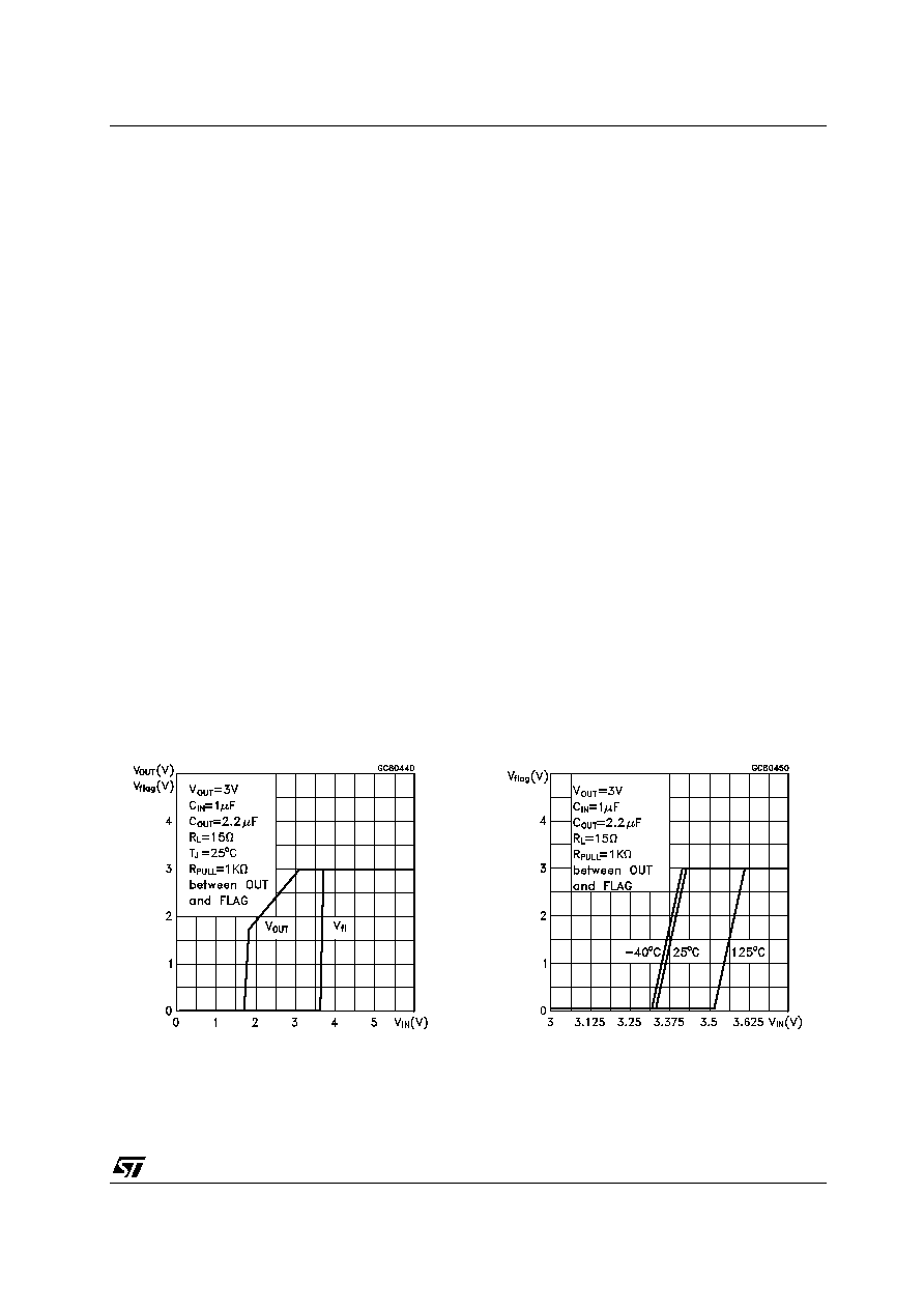
L4987 SERIES
9/13
APPLICATION HINT OF L4987CPT30
HOW TO USE THE CONTROL FLAG
The flag produces a logic "low" whenever the output drops out of regulation. An "out of regulation
condition can result from:
1) Low Input Voltage (V
IN
V
OUT
+ V
DROP
)
2) Current Limiting
3) Thermal Limiting
Figure 1 to 2 show the typical behavior of the output voltage and the control flag versus the input voltage
and the temperature. No hysteresis is implemented; so the response of V
OUT
and V
FLAG
are the same
either when the V
IN
ramps up or down.
The control flag is an open collector which requires an external pull-up resistor. This may be connected to
the regulator output (Figure 9) or some other supply voltage (Figure 10).
Using the regulator output prevents an invalid "high" on the flag which occurs if it is pulled up to an
external voltage while the regulator input voltage is reduced below about 2V (Figure 12).
Concerning the pull-up resistor its value must be properly chosen as suggested below. When "low" as it
is possible to see in figure 6 the control flag voltage is:
V
FLAG(LOW)
= V
CE
= 0.5 = V
SUPPLY
- R
PULL
x I
FL
V
SUPPLY
is chosen by design and, thus is known, while I
FL
must be at maximum 10mA.
Then 0.5V
V
SUPPLY
- R
PULL
x 10mA
The minimum value of R
PULL
, is, so, determined by the following equation:
R
PULL(min)
V
SUPPLY
- 0.5/10 mA
Regarding the maximum value of R
PULL
note that its value depends of the type of logic used (CMOS, TTL
etc.), the transistor leakage current and the presence or not of a load on V
FLAG
.
The following example shows how to determine the R
PULL
max in the case of CMOS logic, no load and
10µA (for L4978 it is the maximum value of I
FH
) of control flag leakage current.
Because of CMOS logic:
V
FLAG(HIGH)
2/3 V
SUPPLY
But:
V
FLAG(HIGH)
= V
SUPPLY
- R
PULL
x I
FH
2/3 V
SUPPLY
so, the maximum value is determined by the following equation:
R
PULL(MAX)
(
1/3 V
SUPPLY
)/10 A
Figure 7 : Output and Flag Voltage vs Input
Figure 8 : Flag Voltage vs Input
L4987 SERIES
10/13
Figure 9 : Test Circuit
Figure 10 : Test Circuit
Figure 11 : Equivalent Output Circuit
Figure 12 : Output and Flag Voltage vs Input

L4987 SERIES
11/13
DIM.
mm.
inch
MIN.
TYP
MAX.
MIN.
TYP.
MAX.
A
2.2
2.4
0.086
0.094
A1
0.9
1.1
0.035
0.043
A2
0.03
0.23
0.001
0.009
B
0.4
0.6
0.015
0.023
B2
5.2
5.4
0.204
0.212
C
0.45
0.6
0.017
0.023
C2
0.48
0.6
0.019
0.023
D
6
6.2
0.236
0.244
E
6.4
6.6
0.252
0.260
G
4.9
5.25
0.193
0.206
G1
2.38
2.7
0.093
0.106
H
9.35
10.1
0.368
0.397
L2
0.8
0.031
L4
0.6
1
0.023
0.039
PPAK MECHANICAL DATA
0078180-B

L4987 SERIES
12/13
DIM.
mm.
inch
MIN.
TYP
MAX.
MIN.
TYP.
MAX.
A
330
12.992
C
12.8
13.0
13.2
0.504
0.512
0.519
D
20.2
0.795
N
60
2.362
T
14.4
0.567
Ao
6.80
6.90
7.00
0.268
0.272
0.2.76
Bo
10.40
10.50
10.60
0.409
0.413
0.417
Ko
2.55
2.65
2.75
0.100
0.104
0.105
Po
3.9
4.0
4.1
0.153
0.157
0.161
P
7.9
8.0
8.1
0.311
0.315
0.319
Tape & Reel DPAK-PPAK MECHANICAL DATA

L4987 SERIES
13/13
Information furnished is believed to be accurate and reliable. However, STMicroelectronics assumes no responsibility for the
consequences of use of such information nor for any infringement of patents or other rights of third parties which may result from
its use. No license is granted by implication or otherwise under any patent or patent rights of STMicroelectronics. Specifications
mentioned in this publication are subject to change without notice. This publication supersedes and replaces all information
previously supplied. STMicroelectronics products are not authorized for use as critical components in life support devices or
systems without express written approval of STMicroelectronics.
The ST logo is a registered trademark of STMicroelectronics
All other names are the property of their respective owners
© 2003 STMicroelectronics - All Rights Reserved
STMicroelectronics GROUP OF COMPANIES
Australia - Belgium - Brazil - Canada - China - Czech Republic - Finland - France - Germany - Hong Kong - India - Israel - Italy - Japan -
Malaysia - Malta - Morocco - Singapore - Spain - Sweden - Switzerland - United Kingdom - United States.
http://www.st.com