 | –≠–ª–µ–∫—Ç—Ä–æ–Ω–Ω—ã–π –∫–æ–º–ø–æ–Ω–µ–Ω—Ç: L4990D | –°–∫–∞—á–∞—Ç—å:  PDF PDF  ZIP ZIP |

L4990
L4990A
PRIMARY CONTROLLER
CURRENT-MODE CONTROL PWM
SWITCHING FREQUENCY UP TO 1MHz
LOW START-UP CURRENT < 0.45mA
HIGH-CURRENT OUTPUT DRIVE SUITABLE
FOR POWER MOSFET (1A)
FULLY LATCHED PWM LOGIC WITH DOU-
BLE PULSE SUPPRESSION
PROGRAMMABLE DUTY CYCLE
100% AND 50% MAXIMUM DUTY CYCLE
LIMIT
PROGRAMMABLE SOFT START
PRIMARY OVERCURRENT FAULT DETEC-
TION WITH RE-START DELAY
PWM UVLO WITH HYSTERESIS
IN/OUT SYNCHRONIZATION
DISABLE LATCHED
INTERNAL 100ns LEADING EDGE BLANK-
ING OF CURRENT SENSE
PACKAGE: DIP16 AND SO16W
DESCRIPTION
This primary controller I.C., developed in BCD60II
technology, has been designed to implement off
line or DC-DC power supply applications using a
fixed frequency current mode control.
Based on a standard current mode PWM control-
ler this device includes some features as pro-
grammable soft start, IN/OUT synchronization,
disable (to be used for over voltage protection
and for power management), precise maximum
Duty Cycle Control, 100ns (typ) leading edge
blanking on current sense, pulse by pulse current
limit and overcurrent protection with soft start in-
tervention.
July 1999
Æ
+
-
+
-
TIMING
2
3
+
-
14
T
Vref
CLK
2.5V
+
-
1.2V
13
BLANKING
PWM
FAULT
SOFT-START
R
S
Q
25V
16V/10V
VREF OK
DIS
+
-
E/A
1V
R
2R
DIS
2.5V
7
6
5
11
10
9
4
8
15
1
13V
PWM UVLO
12
SGND
COMP
SS
ISEN
DIS
DC
RCT
SYNC
DC-LIM
V
CC
VREF
D98IN1002
VFB
PGND
OUT
V
C
OVER CURRENT
BLOCK DIAGRAM
ORDERING NUMBERS: L4990/L4990A(DIP16)
L4990D/L4990AD (SO16W)
MULTIPOWER BCD TECHNOLOGY
DIP16
SO16W
1/24

ABSOLUTE MAXIMUM RATINGS
Symbol
Parameter
Value
Unit
V
CC
Supply Voltage (I
CC
< 50mA) (*)
selflimit
V
I
OUT
Output Peak Pulse Current
1.5
A
Analog Inputs & Outputs (6,7)
-0.3 to 8
V
Analog Inputs & Outputs (1,2,3,4,5,15,14 13)
-0.3 to 6
V
P
tot
Power Dissipation @ T
amb
= 70
∞
C
1
W
T
j
Junction Temperature, Operating Range
-25 to 125
∞
C
T
stg
Storage Temperature, Operating Range
-55 to 150
∞
C
(*) maximum package power dissipation limits must be observed
THERMAL DATA
Symbol
Parameter
Value
Unit
R
th j-amb
Thermal Resistance Junction to Ambient
DIP16
80
∞
C/W
R
th j-amb
Thermal Resistance Junction to Ambient
SO16
120
∞
C/W
PIN FUNCTIONS
N.
Name
Fun ction
1
SYNC
Synchronization. A synchronization pulse terminates the PWM cycle and discharges Ct
2
RCT
Oscillator pin for external C
t
, R
t
components
3
DC
Duty Cycle control
4
VREF
5.0V +/-1.5% reference voltage
5
VFB
Error Amplifier Inverting input
6
COMP
Error Amplifier Output
7
SS
Soft start pin for external capacitor Css
8
V
CC
Supply for internal "Signal" circuitry
9
V
C
Supply for Power section
10
OUT
High current totem pole output
11
PGND
Power ground
12
SGND
Signal ground
13
ISEN
Current sense
14
DIS
Disable. It must never be left floating. Tie to SGND if not used.
15
DC-LIM
Connecting this pin to Vref, DC is limited to 50%. If it is left floating or grounded no limitation is
imposed
16
NC
Not connected
SYNC
RCT
DC
VREF
VFB
SS
COMP
1
3
2
4
5
6
7
OUT
SGND
PGND
ISEN
DIS
DC-LIM
N.C.
16
15
14
13
12
10
11
D95IN197
V
CC
8
V
C
9
PIN CONNECTION
L4990 - L4990A
2/24

ELECTRICAL CHARACTERISTICS (V
CC
= 15V; T
j
= 0 to 70
∞
C; unless otherwise specified.)
Symbol
Parameter
Test Condition
Min.
Typ.
Max.
Unit
REFERENCE SECTION
V
O
Output Voltage
T
j
= 25
∞
C; I
O
= 1mA
4.925
5.0
5.075
V
Line Regulation
V
CC
= 12 to 20V
2.0
15
mV
Load Regulation
I
O
= 1 to 20mA
5.0
20
mV
T
S
Temperature Stability
0.4
mV/
∞
C
Total Variation
Line, Load, Temperature
4.875
5.0
5.125
V
I
OS
Short Circuit Current
Vref = 0V
30
150
mA
Power Down/UVLO
V
CC
= 8.5V; I
sink
= 0.5mA
0.2
0.5
V
OSCILLATOR SECTION
Initial Accuracy
T
j
= 25
∞
C; R
T
= 4.42k
;
C
T
= 1nF; pin 15 Vref
285
300
315
kHz
Accuracy
R
T
= 4.42K
; V
CC
= 12 to 20V;
C
T
= 1nF; pin 15 = Vref
279
300
321
kHz
Initial Accuracy
T
j
= 25
∞
C; R
T
= 4.42K
;
C
T
= 1nF; pin 15 OPEN
280
295
310
kHz
Accuracy
R
T
= 4.42K
; V
CC
= 12 to 20V;
C
T
= 1nF; pin 15 OPEN
275
295
315
kHz
Duty Cycle
pin 3 = 0,7V, pin 15 = Vref
pin 3 = 0.7V, pin 15 = OPEN
0
0
%
%
Duty Cycle
R
T
= 4.42k
C
T
= 1nF
pin 3 = 3.2V, pin 15 = Vref
pin 3 = 3.2V, pin 15 = OPEN
45
90
%
%
Duty Cycle Accuracy
pin 3 = 2.02V, pin 15 = OPEN
37
40
43
%
Oscillator Ramp Peak
3.0
V
Oscillator Ramp Valley
1.0
V
ERROR AMPLIFIER SECTION
Input Bias Current
V
FB
to GND
0.2
1.0
µ
A
V
I
Input Voltage
V
COMP
= V
FB
2.42
2.5
2.58
V
G
OPL
Open Loop Gain
V
COMP
= 2 to 4V
60
90
dB
SVR
Supply Voltage Rejection
V
CC
= 12 to 20V
85
dB
V
OL
Output Low Voltage
I
sink
= 2mA, V
FB
= 2.7V
1.1
V
V
OH
Output High Voltage
I
sou rce
= 0.5mA, V
FB
= 2.3V
5
6
V
I
O
Output Source Current
V
COMP
> 4V, V
FB
= 2.3V
0.5
1.3
mA
Output Sink Current
V
COMP
= 1.1V, V
FB
= 2.7V
2
6
mA
Unit Gain Bandwidth
2
4
MHz
S
R
Slew Rate
8
V/
µ
s
PWM CURRENT SENSE SECTION
I
b
Input Bias Current
I
sen
= 0
3
15
µ
A
I
S
Maximum Input Signal
V
COMP
= 5V
0.92
1.0
1.08
V
Delay to Output
100
ns
Gain
2.85
3
3.15
V/V
SOFT START
I
SSC
SS Charge Current
14
20
26
µ
A
I
SSD
SS Discharge Current
VSS = 0.6V
200
µ
A
V
SSSAT
SS Saturation Voltage
DC = 0%
0.6
V
V
SSCLAMP
SS Clamp Voltage
7
V
LEADING EDGE BLANKING
Internal Masking Time
100
ns
L4990 - L4990A
3/24

FUNCTIONAL DESCRIPTION
The I.C. contains a standard PWM current mode
control section with improved performance with
respect to the UC384X family.
Enhanced features include start-up bias current
reduced to < 270
µ
A (typ), improved E/A perform-
ance (4MHz B/W, 1.3mA Source Current, high-
slew rate) accurate 1MHz oscillator, and also re-
duced propagation delays in the critical path from
Current Sense to Output.
ADDITIONAL FEATURES
Soft Start (SS)
An external capacitor is charged by an internal
constant current source (20
µ
A) to generate a SS
signal which clamps the E/A output
The SS pin doubles as a Fault Reset Delay func-
tion as described below.
Current Limit / Reset Delay
An internal high-speed current limit comparator
ELECTRICAL CHARACTERISTICS (continued.)
Symbol
Parameter
Test Condition
Min.
Typ.
Max.
Unit
OUTPUT SECTION
V
OL
Output Low Voltage
I
O
= 250mA
1.0
V
V
OH
Output High Voltage
I
O
= 20mA; V
CC
= 12V
10
10.5
V
I
O
= 200mA; V
CC
= 12V
9
10
V
V
OUT CLAMP
Output Clamp Voltage
I
O
= 5mA; V
CC
= 20V
13
V
Collector Leakage
V
CC
= 20V V
C
= 24V
100
200
µ
A
Fall Time
C
O
= 1nF
C
O
= 2.5nF
20
35
60
ns
ns
Rise Time
C
O
= 1nF
C
O
= 2.5nF
50
70
100
ns
ns
UVLO Saturation
V
CC
= 0V to V
CCON
; I
sink
= 10mA
1.0
V
SUPPLY SECTION
V
CCON
Startup voltage
L4990
L4990A
15
7.8
16
8.4
17
9
V
V
V
CCOFF
Minimum Operating Voltage
L4990
L4990A
9
7
10
7.6
11
8.2
V
v
V
hys
Voltage After Turn-on Hysteresis
L4990
L4990A
5.5
0.5
6
0.8
V
v
I
S
Start Up Current
Before Turn-on at:
V
CC
= V
CCON
- 0.5V
100
270
450
µ
A
I
op
Operating Current
C
T
= 1nF, R
T
= 4.42k
, C
O
=1nF
12
18
mA
I
q
Quiescent Current
(After turn on), Co =0nF
C
T
= 1nF, R
T
= 4.42k
,
7.0
10
mA
I
SH
Shutdown Current
100
270
450
µ
A
V
Z
Zener Voltage
I
8
= 20mA
21
25
30
V
SYNCHRONIZATION SECTION
Master Operation
V
1
Clock Amplitude
I
SOURCE
= 0.8mA
4
V
I
1
Clock Source Current
Vclock = 3.5V
7
mA
Slave Operation
V
1
Sync Pulse
Low Level
1
V
High Level
3.5
V
I
1
Sync Pulse Current
VSYNC = 3.5V
0.8
mA
OVER CURRENT PROTECTION
V
t
Fault Threshold Voltage
1.1
1.2
1.3
V
DISABLE SECTION
Shutdown threshold
2.4
2.5
2.6
V
L4990 - L4990A
4/24
referenced to 1.2V detects primary over-current
conditions. On detection of an overcurrent fault
the output is immediately shutdown and the fault
is also latched. A Fault Reset Delay is imple-
mented by discharging the external Soft Start
(SS) timing capacitor
before resetting the fault
latch and initiating a softstart cycle.
In case of a continuous fault condition the SS ca-
pacitor is charged to 5V before being discharged
again, to ensure that the fault frequency does not
exceed the programmed soft start frequency.
Duty Cycle Limit
A simple connection between the DC-LIM and the
available Vref activates an internal T- FlipFlop lim-
iting the DC to about 50%. If this pin is not con-
nected or grounded, the limit of the duty cycle is
extended to about 100%
Duty Cycle Control
Duty Cycle DC is externally programmed by set-
ting a voltage between 1V (0% DC) and 3V
(100% DC) at the DC pin. The programmed volt-
age is compared with the oscillator C
T
capacitor
charging waveform to determine the maximum
ON-time in each period. This function gives a fine
control of DC.
If this pin is floating the maximum duty cycle de-
pends on DC-LIM status.
Synchronization
A SYNC pin eases Synchronization of the IC to
the external world ( e.g.
another IC working in
parallel or to TV/monitor sync signal).
In TV/monitor applications the timing components
R
T
, C
T
are set for a frequency lower than the
minimum TV sync frequency. When the TV circuit
has powered-up it takes over and the system fre-
quency is that of the SYNC. Duty Cycle is control-
lable using the DC function.
In parallel operation of several IC's no Mas-
ter/Slave designation is required as the higher fre-
quency IC is automatically the master. Controllers
to be synchronized have their SYNC pins tied to-
gether and each SYNC pin operates as a bidirec-
tional circuit. The first IC to drive its SYNC pin is
the master and it initiates a discharge of the C
T
timing capacitor of every controller. The Sync in-
put signal is edge-triggered and sets an internal
"sync latch" which ensures full discharge of C
T
.
Disable Function
The DIS pin performs a logic level latched-shut-
down function. When pulled above 2.5V it shuts
down the complete IC with a standby current of
<270
µ
A (typ).
To reset the IC the V
CC
pin must be pulled-down
below the lower UVLO threshold (10V).
Leading Edge Blanking (LEB)
An LEB interval of 100ns has been incorporated
into the IC to blank out the current sense signal
during the first 100ns from switch turn-on.
This provides noise immunity to turn-on spikes
and reduces external RC filtering requirements on
the current-sense signal.
6
8
2 0
3 0
V1 4 = 0 , O SC= d isa bled
T j = 25
∞
C
0
4
8
1 2
1 6
2 0
2 4
0
0 .2
0 .4
0 .6
0 .8
1
V c c [V]
Iq [m A ]
X
Y
Figure 1. Quiescent current vs. input voltage.
(X = 7.6V and Y = 8.4V for L4990A)
8
10
12
14
16
18
20
22
24
21 0
24 0
27 0
30 0
Vcc
[V ]
Iq
[uA]
V14 = Vref
T j = 25
∞
C
Figure 2. Quiescent current vs. input voltage
(after disable).
L4990 - L4990A
5/24

8
10
12
14
16
18
20
22
24
7.0
7.5
8.0
8.5
9.0
V cc
[V ]
Iq [m A ]
V 14 = 0, V5 = Vr ef
Rt = 4.5Kohm,Tj = 25
∞
C
5 0 0K h z
3 0 0K h z
1M h z
1 0 0 Kh z
Figure 3. Quiescent current vs. input voltage.
-50
-25
0
25
50
75
100
125
150
4.9
4.95
5
5.05
5.1
Tj (
∞
C)
Vref [V])
Vcc = 15V
Iref = 1mA
Figure 7. Vref vs. junction temperature.
-50
-25
0
25
50
75
100
125
150
4.9
4.95
5
5.05
5.1
Tj (
∞
C)
Vref [V]
Vcc = 15V
Iref= 20mA
Figure 8. Vref vs. junction temperature.
8
10
12
14
16
18
20
22
0
6
12
18
24
30
36
Vcc [V]
Iq [mA]
Co = 1nF, Tj = 25
∞
C
DC = 1 00%
1M H z
50 0KH z
3 00KH z
10 0KH z
Figure 5. Quiescent current vs. input voltage
and switching frequency.
0
5
10
15
20
25
4.9
4.95
5
5.05
5.1
Iref [mA]
Vref [V]
Vcc=15V
Tj = 25
∞
C
Figure 6. Reference voltage vs. load current.
8
10
12
14
16
1 8
20
22
0
6
12
18
24
30
36
V c c [V ]
I q [mA ]
C o = 1 n F, Tj = 2 5
∞
C
D C = 0 %
1M Hz
500K Hz
300K Hz
100KHz
Figure 4. Quiescent current vs. input voltage
and switching frequency.
L4990 - L4990A
6/24

-50
-25
0
25
50
75
100
125
150
280
290
300
310
320
Tj (
∞
C)
fsw (KHz)
Rt= 4.5Kohm, Ct = 1nF
Vcc = 15V, V15=Vref
Figure 14. Switching frequency vs. temperature.
10
0
0.2
0.4
0.6
0.8
1
1.2
6
8
10
12
14
16
Isourc e [A]
V sat = V [V]
Vcc = 15V
Tj = 25
∞
C
Figure 10. Output saturation.
0
0.2
0.4
0.6
0.8
1
1.2
0
0.5
1
1.5
2
2.5
Is ink [A]
10
Vsat = V
[V ]
Vcc = 15V
Tj = 25
∞
C
Figure 11. Output saturation.
1
10
100
1000
10000
0
40
80
120
fsw (Hz)
SVRR (dB)
Vcc=15V
Vp-p=1V
Figure 9. Vref SVRR vs. switching frequency.
10
20
30
40
10
20
50
100
200
500
1000
2000
5000
Rt (kohm)
fsw(KHz)
100pF
220pF
470pF
1nF
2.2nF
5.6nF
Tj= 25
∞
C
Vcc =15V, V15 =0V
Figure13. Timingresistorvs.switchingfrequency.
0
200
400
600
800
1,000 1,200 1,400
0
10
20
30
40
50
Vpin10 [mV]
Ipin10 [mA]
Vcc < Vccon
before turn-on
Figure 12. UVLO Saturation
L4990 - L4990A
7/24

0.01
0.1
1
10
100
1000
10000 100000
0
50
100
150
20
40
60
80
100
120
140
f (KHz)
G [dB]
Phase
Figure 19. E/A frequency response.
0
10
20
30
40
50
60
70
80
90 100
1
1.5
2
2.5
3
3.5
Duty C y cle [% ]
DC Control Voltage V pin3 [V]
Rt = 4.5Kohm ,
Ct = 1nF
V15 = 0 V
V1 5 = Vr ef
Figure 17. Maximum Duty Cycle vs Vpin3.
-50
-25
0
25
50
75
100
125
150
60
70
80
90
100
110
120
130
Tj (
∞
C)
Delay to output (ns)
PIN10 = OPEN
1V pulse
on PIN13
Figure18.Delayto output vs junctiontemperature.
-50
-25
0
25
50
75
100
125
150
280
290
300
310
320
Tj (
∞
C)
fsw (KHz)
Rt= 4.5Kohm, Ct = 1nF
Vcc = 15V, V15= 0
Figure 15. Switching frequency vs. temperature.
2
4
6
8
10
300
600
900
1,200
1,500
Timing capacitor Ct [nF]
Dead time [ns]
Rt =4.5Kohm
V15 = 0V
V15 = Vref
Figure 16. Dead time vs Ct.
L4990 - L4990A
8/24

APPLICATION INFORMATION
Detailed Pin Functions Description
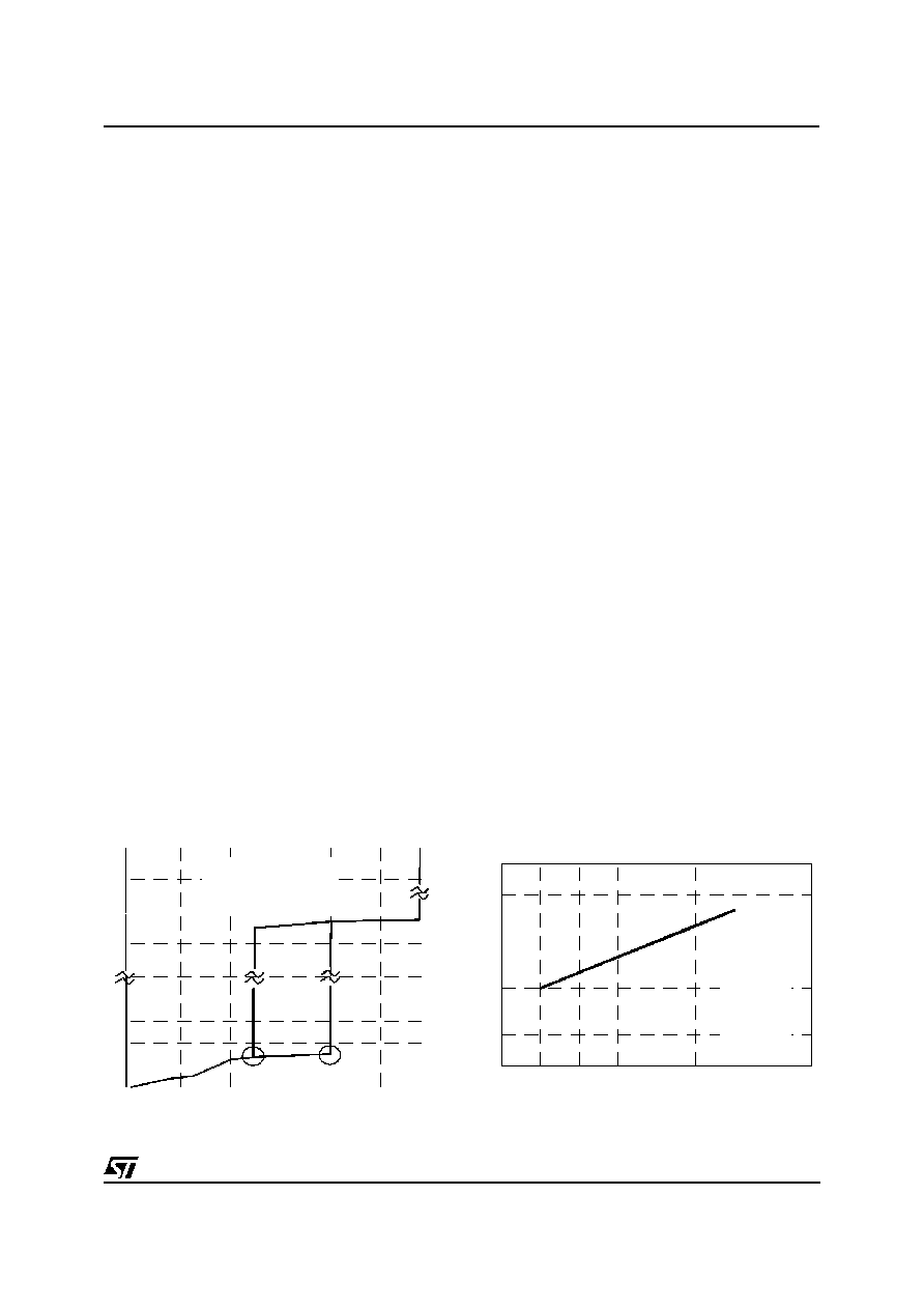
Pin 1. SYNC (In/Out Synchronization). This func-
tion allows the IC's oscillator either to synchronize
other controllers (master) or to be synchronized to
an external frequency (slave).
As a master, the pin delivers positive pulses dur-
ing the ramp-down of the oscillator (see pin 2). In
slave operation the circuit is edge triggered. Refer
to fig. 21 to see how it works. When several IC
work in parallel no master-slave designation is
needed because the fastest one becomes auto-
matically the master.
During the ramp-up of the oscillator the pin is
pulled low by a 600
µ
A generator. During the
ramp-down, that is when the pulse is released,
the 600
µ
A pull-down is disconnected. The pin be-
comes a generator whose source capability is
typically 7mA (with a voltage still higher than
3.5V).
In fig. 20, some practical examples of synchroniz-
ing the L4990 are given.
L4990
L4990
R
T
VREF
SYNC
SYNC
RCT
RCT
L4981A
(MASTER)
L4990
(SLAVE)
R
T
VREF
SYNC
RCT
R
OSC
C
OSC
C
T
L4990
(MASTER)
L4981A
(SLAVE)
SYNC
R
OSC
C
T
C
OSC
SYNC
(a)
(b)
(c)
R
T
D97IN494A
C
T
VREF
4
1
2
1
2
16
18
17
4
2
1
RCT
1
2
4
16
17
18
Figure 20. Synchronizing the L4990.
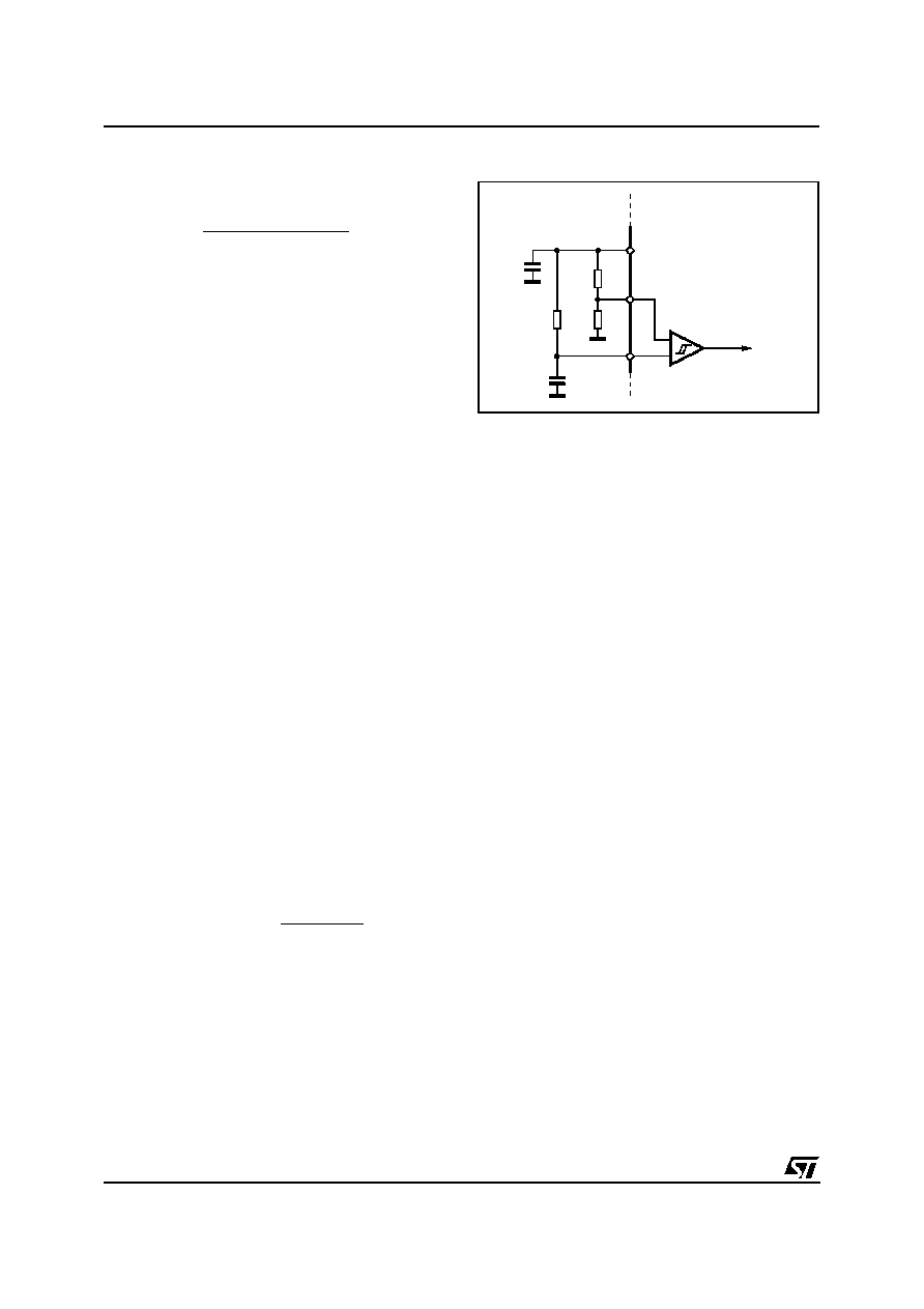
Pin 2. RCT (Oscillator). A resistor (R
T
) and a ca-
pacitor (C
T
), connected as shown in fig. 21 set the
operating frequency f
osc
of the oscillator.
C
T
is charged through R
T
until its voltage reaches
3V, then is quickly internally discharged. As the
voltage has dropped to 1V it starts being charged
again
+
-
R2
R3
R1
CLAMP
D1
50
R
T
C
T
D
R
Q
600
µ
A
D97IN500B
V
REF
RCT
SYNC
CLK
2
4
1
Figure 21. Oscillator and synchronization internal schematic.
L4990 - L4990A
9/24
The frequency can be established with the aid of
fig. 13 diagrams or considering the approximate
relationship:
f
osc
1
C
T
(
0.693
R
T
+
K
T
)
(
1
)
where K
T
is defined as:
K
T
=
90, V
15
=
VREF
160 V
15
=
GND/OPEN
(
2
)
and is linked to the duration of the falling edge of
the sawtooth:
T
d
30
10
-9
+ K
T
C
T
(3)
T
d
is also the duration of the sync pulses deliv-
ered at pin 1 and defines the upper extreme of
the duty cycle range, D
x
(see pin 15 for D
x
defini-
tion and calculation).
In case V
15
is connected to VREF, however, the
switching freque ncy of the system will be as
high as half f
osc
.
If the IC is to be synchronized to an external oscil-
lator, R
T
and C
T
should be selected for a f
osc
lower than the master frequency in any condition
(typically, 10-20% ), depending on the tolerance
of R
T
and C
T
itself.
Pin 3. DC (Duty Cycle Control). By biasing this
pin with a voltage between 1 and 3 V it is possible
to set the maximum duty cycle between 0 and the
upper extreme D
x
(see pin 15).
If D
max
is the desired maximum duty cycle, the
voltage V3 to be applied to pin 3 is:
V
3
= 5 - 2
(2-Dmax)
(4)
D
max
is determined by internal comparison be-
tween V3 and the oscillator ramp (see fig. 22),
thus in case the device is synchronized to an ex-
ternal frequency f
ext
(and therefore the oscillator
amplitude is reduced), (4) changes into:
V
3
=
5
-
4
exp
-
D
max
R
T
C
T
f
ext
(5)
A voltage below 1V will inhibit the driver output
stage. This could be used for a not-latched device
disable, for example in case of overvoltage pro-
tection (see application ideas).
If no limitation on the maximum duty cycle is re-
quired (i.e. D
MAX
= D
X
), the pin has to be left float-
ing. An internal pull-up holds the voltage above
3V. Should the pin pick up noise (e.g. during ESD
tests), it can be connected to V
REF
through a
4.7k
resistor.
Pin 4. VREF (Reference Voltage). An internal
generator furnishes an accurate voltage reference
(5V
±
1.5%) that can be used to supply an external
circuit (consider some ten mA).
A small film capacitor (1
µ
F typ.), connected be-
tween this pin and SGND, is recommended to
preventswitching noise from affecting the reference.
Before device turn-on, this pin has a sink current ca-
pability of 0.5mA.
Pin 5. VFB (Error Amplifier Inverting Input). The
feedback signal is applied to this pin and is com-
pared to the E/A internal reference (2.5V). The
E/A output generates the control voltage which
fixes the duty cycle.
The E/A features high gain-bandwidth product,
which allows to broaden the bandwidth of the
overall control loop, high slew-rate and current
capability, which improves its large signal behav-
ior. Usually the compensation network, which sta-
bilizes the overall control loop, is connected be-
tween this pin and COMP (pin 6).
Pin 6. COMP (Error Amplifier Output). Usually,
this pin is used for frequency compensation and
the relevant network is connected between this
pin and VFB (pin 5). Compensation networks to-
wards ground are not possible since the L4990
E/A is a voltage mode amplifier (low output im-
pedance). See application ideas for some exam-
ple of compensation techniques.
Pin 7. SS (Soft-Start). At device start-up, a ca-
pacitor (Css) connected between this pin and
SGND (pin 12) is charged by an internal current
generator, ISSC, up to about 7V. During this
ramp, the E/A output is clamped by the voltage
across Css itself and allowed to rise linearly, start-
ing from zero, up to the steady-state value im-
posed by the control loop. The maximum time in-
terval during which the E/A is clamped, referred to
as soft-start time, is approximately:
+
-
R2
R1
R
T
C
T
D97IN501A
V
REF
RCT
DC
TO PWM LOGIC
4
3
2
Figure 22. Duty cycle control.
L4990 - L4990A
10/24
T
ss
3
R
sense
I
Qpk
I
SSC
C
ss
(6)
where R
sense
is the current sense resistor (see pin
13) and I
Qpk
is the switch peak current (flowing
through R
sense
), which depends on the output
load. Usually, C
SS
is selected for a T
SS
in the or-
der of milliseconds.
As mentioned before, the soft-start intervenes
also in case of severe overload or short circuit on
the output. Referring to fig. 23, pulse-by-pulse
current limitation is somehow effective as long as
the ON-time of the power switch can be reduced
(from A to B). After the minimum ON-time is
reached (from B onwards) the current is out of
control.
To prevent this risk, a comparator trips an over-
current handling procedure, named 'hiccup' mode
operation, when a voltage above 1.2V (point C) is
detected on current sense input (ISEN, pin 13).
Basically, the IC is turned off and then soft-started
as long as the fault condition is detected. As a re-
sult, the operating point is moved abruptly to D,
creating a foldback effect. Fig. 24 illustrates the
operation.
The oscillation frequency appearing on the soft-
start capacitor in case of permanent fault, referred
to as 'hiccup" period, is approximately given by:
T
hic
4.5
1
I
SSC
+
1
I
SSD
C
ss
(
7
)
Since the system tries restarting each hiccup cy-
cle, there is not any latchoff risk.
V
OUT
T
ON
D.C.M.
C.C.M.
D
A
B
C
I
Qpk
T
ON(min)
1-2 ∑I
Qpk
I
Qpk(max)
I
OUT
I
SHORT
I
OUT(max)
D97IN495
Figure 23. Regulation characteristic and re-
lated quantities
7V
T
hic
time
SHORT
I
OUT
I
SEN
FAULT
SS
5V
0.5V
D97IN496
Figure 24. Hiccup mode operation.
L4990 - L4990A
11/24

"Hiccup" keeps the system in control in case of
short circuits but does not eliminate power com-
ponents overstress during pulse-by-pulse limita-
tion (from A to C). Other external protection cir-
cuits are needed if a better control of overloads is
required.
Pin 8. VCC (Controller Supply). This pin supplies
the signal part of the IC. The device is enabled as
VCC voltage exceeds the start threshold and
works as long as the voltage is above the UVLO
threshold. Otherwise the device is shut down and
the current consumption is extremely low.
An internal Zener limits the voltage on VCC to
25V. Below this value the IC current consumption
is low but increases considerably if this limit is ex-
ceeded.
A small film capacitor between this pin and SGND
(pin 12), placed as close as possible to the IC, is
recommended to filter high frequency noise.
Pin 9. VC (Supply of the Power Stage). It sup-
plies the driver of the external switch and there-
fore absorbs a pulsed current. Thus it is recom-
mended to place a buffer capacitor (towards
PGND, pin 11, as close as possible to the IC)
able to sustain these current pulses and in order
to avoid them inducing disturbances.
This pin can be connected to the buffer capacitor
directly or through a resistor, as shown in fig. 25,
to control separately the turn-on and turn-off
speed of the external switch, typically a Power-
MOS. At turn-on the gate resistance is R
g
+ R
g'
and turn-off is R
g
only.
Pin 10. OUT (Driver Output). This pin is the out-
put of the driver stage of the external power
switch. Usually, this will be a PowerMOS, al-
though the driver is powerful enough to drive
BJT's (1.6A source, 2A sink, peak).
The driver is made up of a totem pole with a high-
side NPN Darlington and a low-side VDMOS, and
delivers a voltage internally clamped, as shown in
fig. 25. Thus it is possible to supply the driver (pin
9) with higher voltages without any problem of
damage for the gate oxide of the external MOS,
but, of course, the power dissipation on the IC will
increase.
In UVLO conditions an internal circuit (shown in
fig.26) holds the pin low in order to ensure that
the external MOS cannot be turned on acciden-
tally. The peculiarity of this circuit is its ability to
mantain the same sink capability (typically, 20mA
@ 1V) from V
CC
= 0V up to the start-up threshold.
When the threshold is exceeded and the L4990
starts operating, V
REFOK
is pulled high (refer to
fig. 26) and the circuit is disabled.
It is then possible to omit the "bleeder" resistor
(connected between the gate and the source of
the MOS) ordinarily used to prevent undesired
switching-on of the external MOS because of
some leakage current.
Pin 11. PGND (Power Ground). The current loop
during the discharge of the gate of the external
MOS is closed through this pin. This loop should
be as short as possible to reduce EMI and run
separately from signal currents return.
Pin 12. SGND (Signal Ground). This ground ref-
erences the control circuitry of the IC, so all the
ground connections of the external parts related
to control functions must lead to this pin. In laying
out the PCB, care must be taken in preventing
switched high currents from flowing through the
SGND path.
Pin 13. ISEN (Current Sense). This pin is to be
connected to the "hot" lead of the current sense
resistor R
sense
(being the other one grounded), to
get a voltage ramp which is an image of the cur-
rent of the switch, (I
Q
). When this voltage is equal
to:
OUT
Rg
DRIVE &
CONTROL
13V
V
C
V
CC
Rg'
PGND
Rg(ON)=Rg+Rg'
Rg(OFF)=Rg
D97IN497A
L4990
9
10
11
8
17
13
(V)
Figure25.Turn-on and turn-off speeds adjustment
10
12
SGND
OUT
V
REFOK
D97IN538
Figure 26. Pull-Down of the output in UVLO.
L4990 - L4990A
12/24

V
13pk
=
I
Qpk
R
sense
= (
V
COMP
-
1.4
)
3
(
8
)
the conduction of the switch is terminated.
To increase the noise immunity, a "Leading Edge
Blanking" of about 100ns is internally realized as
shown in fig. 27. Because of that, the smoothing
RC filter between this pin and R
sense
could be re-
moved or, at least, considerably reduced.
+
-
I
D97IN503
ISEN
0
3V
CLK
2V
+
-
+
-
1.2V
FROM E/A
OVERCURRENT
COMPARATOR
PWM
COMPARATOR
TO PWM
LOGIC
TO FAULT
LOGIC
13
Figure 27. Internal LEB
Pin 14. DIS (Device Disable). When the voltage
on pin 14 rises above 2.5V the IC is shut down
and it is necessary to pull VCC (IC supply volt-
age, pin 8) below the UVLO threshold to allow the
device to restart. When disabled, the current con-
sumption of the IC is as low as before start-up.
The pin can be driven by an external logic signal
in case of power management, as shown in fig.
28. It is also possible to realize an overvoltage
protection, as shown in the section " Application
Ideas".
If used, bypass this pin to ground with a filter ca-
pacitor to avoid spurious activation due to noise
spikes. If not, it is advisable to connect the pin to
SGND, even though it might be left floating.
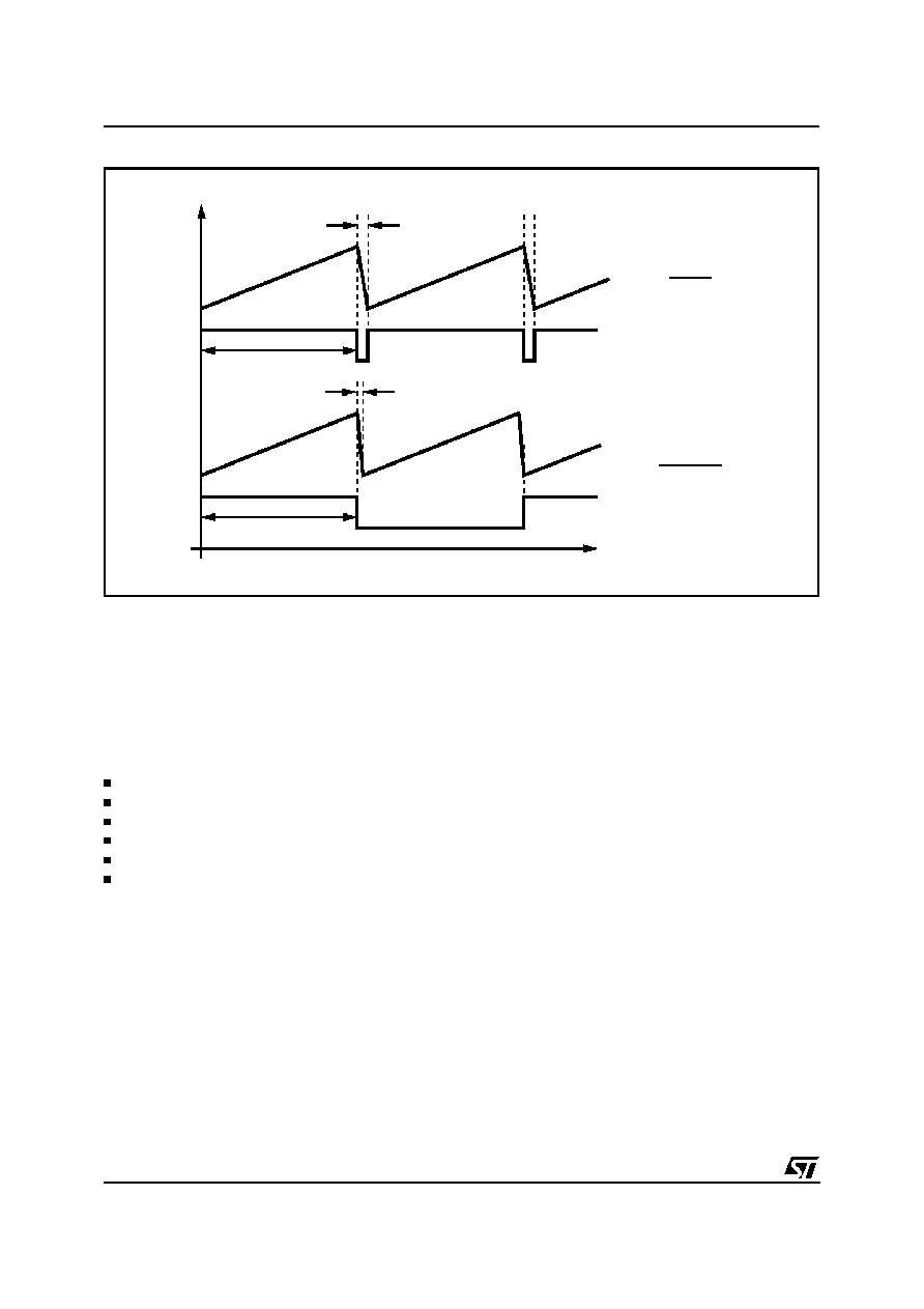
Pin 15. DC-LIM (Maximum Duty Cycle Limit). The
upper extreme, Dx, of the duty cycle range de-
pends on the voltage applied to this pin. Approxi-
mately,
D
x
R
T
R
T
+
230
(
9
)
if DC-LIM is grounded or left floating. Instead,
connecting DC-LIM to VREF (half duty cycle op-
tion), Dx will be set approximately to:
D
x
R
T
2
R
T
+
260
(
10
)
and the output switching frequency will be halved
with respect to the oscillator one because an in-
ternal T flip-flop (see block diagram, fig. 1) is acti-
vated. Fig. 29 shows the operation.
The half duty cycle option speeds up the dis-
charge of the timing capacitor C
T
(in order to get
duty cycles as close as possible to 50%) so the
oscillator frequency - with the same R
T
and C
T
-
will be slightly higher.
The halving of frequency can be used to reduce
losses at light load in all those systems that must
comply with requirements regarding energy con-
sumption (e.g. monitor displays).
+
-
C
D97IN502
DIS
D
R
Q
DISABLE
UVLO
2.5V
14
DISABLE
SIGNAL
Figure 28. Disable (Latched)
L4990 - L4990A
13/24
DEMONSTRATION BOARD
To evaluate the device performance, a demon-
stration board has been realized. Despite its sim-
plicity, it exploits most of the features of the
L4990.
The board embodies an application based on the
following specification of universal mains AC-DC
adapter:
Input voltage range: 85-270 Vac (50/60 Hz)
Output voltage: 15 V
Output current: 0.5 to 2A
Output voltage ripple : 300 mV (max.)
Load regulation:
±
5% (0.5 to 2 A load change)
Target efficiency @ Iout = 2 A: ; 80% over the
input voltage full range
Some preliminary decisions, concerning topology,
operating mode, switching frequency, maximum
duty cycle allowed and control technique, have
been made.
As for topology, at this power level and output
voltage, flyback is the most advantageous one,
mainly because of its simplicity, which means low
parts count, low cost and inherent high efficiency.
A peculiar design choice aiming at optimizing the
overall system concerns the operating mode: the
converter will work in continuous current mode at
low input voltages, when input current is greater,
and in discontinuous mode at higher input volt-
ages. Numerous benefits originate from that.
Compared to discontinuous current mode, con-
tinuous operation involves lower peak currents
(typ. -40%) at the same throughput power. This
implies less stress for all power components.
The transformer inductance is higher and, there-
fore, a smaller air gap is required for a given core:
this increases primary-to-secondary coupling and,
as a consequence, reduces leakage inductance
and improves energy transfer. Both efficiency and
load regulation will take advantage of that.
Another point in favor is a reduction of the mini-
mum output power that the system is able to de-
liver keeping the output well regulated.
Few components are required in addition for
slope compensation.
Actually, continuous mode flyback suffers also
from a poor dynamic behavior during load tran-
sients because of the narrow bandwidth of the
control loop due to stability problems. However,
great dynamic performance is not required to AC-
DC adapters, so this problem is of no concern.
The boundary between the two operating modes
has been set at about 150 Vac (@ Iout=2A).
The selection of the switching frequency is a mat-
ter of trade-off between achieving a small trans-
former size and high efficiency. 200 kHz seems to
be a good compromise.
In this application, the wide input voltage range
requires a large duty cycle sweep. The higher is
the maximum duty cycle, the larger is the operat-
V15=GND
V5=V13=GND
V15=VREF
V5=V13=GND
t
d
t
d
tc
tc
V2
V10
V2
V10
D
X
=
tc
tc + td
D
X
=
tc
2 ∑tc + td
D97IN498
Figure 29. Half duty cycle option.
L4990 - L4990A
14/24

ing conditions range, in terms of input voltage and
output current, that the converter is able to cover
but, on the other hand, the higher is the peak cur-
rent on the secondary side.
As to this point, the L4990 turns out to be particu-
larly useful since it allows to set any maximum
duty cycle greater (and lower) than 50% with very
good precision. In the present case, a maximum
duty cycle of 60% for steady state operation has
been selected and an extra 5% is allowed to take
transients into account.
Since it is not requested a very tight tolerance on
the output, the feedback employs a primary side
voltage sensing technique to reduce cost and
complexity of the circuit. The same technique has
been used to protect against output overvoltages.
The electric schematic is shown in fig. 30. The
PCB layout is shown in figg. 31 and 32. Table 1
and 2 summarize typical system performance,
while table 3 lists the relevant bill of material,
where details are given only for critical compo-
nents and/or where useful.
Warning: the NTC for inrush current limitation is
not assembled, thus use caution when connecting
the demo board to the mains directly. The use of
a variac or an isolation transformer is recom-
mended.
Table 1. System efficiency.
I
out
= 1A
I
out
= 2A
V
in
(Vac)
V
out
(V)
Effic. %
V
ou t
(V)
Effic. %
85
14.93
83.7
14.53
84.3
110
14.95
82.5
14.55
84.9
220
14.95
81.4
14.57
85.2
270
14.96
76
14.59
81.6
Table 2. System performance.
Line regulation
V
in
= 85 to 270 Vac
I
out
= 0.5A
30mV
Load regulation
I
out
= 0.5A to 2A
V
in
= 85 Vac
V
in
= 270 Vac
0.95V
0.90V
Maximum effic.
V
in
= 190 Vac
I
out
= 2A
86.2%
Output ripple
V
in
= 85 to 270 Vac
I
out
= 2A
< 200mV
Minimum load
V
in
= 270 Vac
V
out
< 20V
150mA
Transition Volt.
From C.C.M to D.C.M
I
out
= 2A
160V
85 to
270
Vac
B1
C1
R12
R19
C8
NTC
10
R7
13
R24
15
12
R11
8
14
6
R6
R15
R2
4
3
2
R9
C4
R10
7
R23
Q1
R16
C12
D3
D4
C2
R17
GND
D97IN499B
L4990
R13
R1
C10
C13
D2
R14
R5
C3
R3
C7
R4
5
9
DCC
R8
VREF
C5
C6
Q2
RCT
SS
R22
C15
DC-LIM
SGND
C14
R20
R21
C11
11
PGND
ISEN
OUT
VC
VCC
DIS
COMP
VFB
T1
15V/2A
D1
Figure 30. AC-DC adaptor electric schematic
L4990 - L4990A
15/24
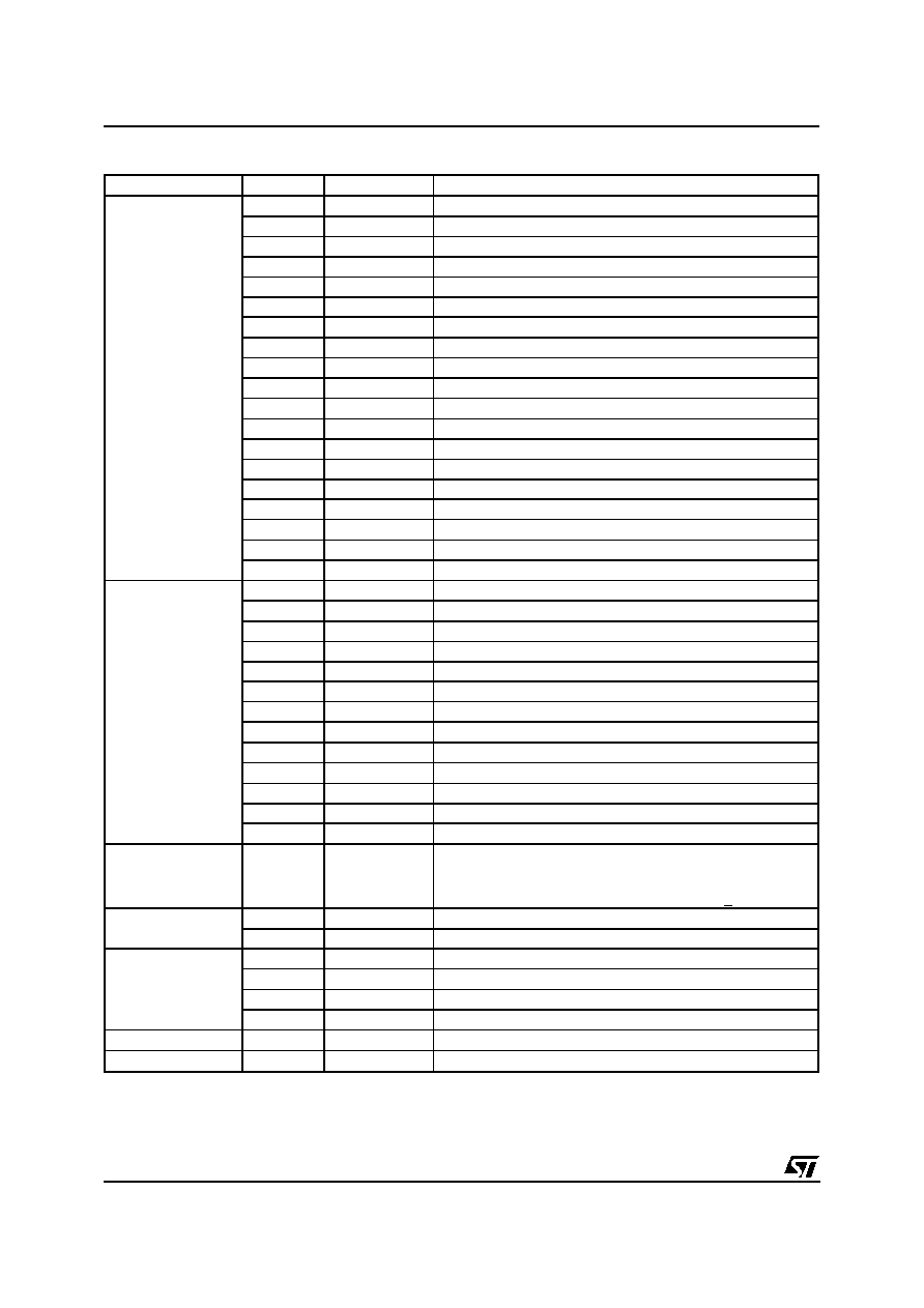
Table 3. Components List of the Fig. 30 AC-DC adaptor electric schematic.
Component
Reference
Value
Description
Resistors
R1
1.6k
2%, 1/8W
R2
9.1k
2%, 1/8W
R3, R14
10
5%, 1/8W
R4
360k
2%, 1/8W
R5
27k
2%, 1/8W
R6
200k
2%, 1/8W
R7
4.7
2%, 1/8W
R8, R9
4.7k
2%, 1/8W
R10
5.6k
2%, 1/8W
R11
1
2%, 1/2W, metallic film (low inductance)
R12, R13
24k
2%, 1/2W
R15
330
5%, 1/8W
R16
-
Not used
R17
390
5%,1W, 2 paralleled resistors (not used)
R19
100k
5%, 1W
R20, R21
470k
2%, 1/8W
R22
200
5%, 1/8W
R23
2k
2%, 1/8W
R24
1k
5%, 1/8W
Capacitors
C1
100
µ
F
400V, NCC-SMH or equiv.
C2
330
µ
F
25V, NCC-LXF or equiv., 3 paralleled capacitors
C3
47
µ
F
25V, electrolytic
C4
1
µ
F
10V, electrolytic
C5
1nF
J precision
C6, C15
10nF
C7, C14
330pF
C8
330pF
160V, polypropilene
C9
100nF
C10
220nF
C11
100pF
ceramic
C12
-
Not used
C13
4.7nF
630V
Transformer
T1
380
µ
H
Core: EFD25, Philips, 3F3 ferrite (or equivalent)
Primary: 46 T, litz wire 20 x 0.1, interleaved assembly
Secondary: 6 T, 4 paralleled litz wire 20 x 0.1
Auxiliary: 7 T (evenly spaced),
0.2 mm GAP ~ 0.7mm
Transistors
Q1
STP5NA80
ST, TO220 package
Q2
2N2222
ST (or equivalent)
Diodes
B1
DF04M
GI (or equivalent)
D1
STPS20100CT
ST, Shottky, TO220 package
D2, D3
1N4148
ST (or equivalent)
D4
BYT11-600
ST, F126 package
Fuse
Fuse
T2A250V
ELU (or equivalent)
NTC
NTC
-
Not used (see warning)
L4990 - L4990A
16/24

Figure 31. AC-DC adaptor PCB layout (1.25 :1 scale) - Component Side.
Figure 32. AC-DC adaptor PCB layout (1.25 :1 scale) - Back Side.
L4990 - L4990A
17/24

Layout hints. Generally speaking a proper cir-
cuitboard layout is vital for correct operation but is
not an easy task. Careful component placing, cor-
rect traces routing, appropriate traces widths and,
in case of high voltages, compliance with isolation
distances are the major issues. The L4990 eases
this task by putting two pins at disposal for sepa-
rate current returns of bias (SGND) and switch
drive currents (PGND) The matter is complex and
only few important points will be here reminded.
1) All current returns (signal ground, power
ground, shielding, etc.) should be routed sepa-
rately and should be connected only at a single
ground point.
2) Noise coupling can be reduced by minimizing
the area circumscribed by current loops. This
applies particularly to loops where high pulsed
currents flow.
3) For high current paths, the traces should be
doubled on the other side of the PCB whenever
possible: this will reduce both the resistance
and the inductance of the wiring.
4) Magnetic field radiation (and stray inductance)
can be reduced by keeping all traces carrying
switched currents as short as possible.
5) In general, traces carrying signal currents
should run far from traces carrying pulsed cur-
rents or with quickly swinging voltages. From
this viewpoint, particular care should be taken
of the high impedance points (current sense in-
put, feedback input, ...). It could be a good idea
to route signal traces on one PCB side and
power traces on the other side.
6) Provide adequate filtering of some crucial
points of the circuit, such as voltage refer-
ences, IC's supply pins, etc.
APPLICATION IDEAS
Here follows a series of ideas/suggestionsaimed at
either improving performance or solving common
application problems of L4990-basedsupplies.
D97IN504
L4990
PGND
ISEN
OUT
V
C
SGND
V
IN
ISOLATION
BOUNDARY
10
9
13
11
12
Figure 33. Isolated MOSFET Drive & Current Transformer Sensing in 2-switch Topologies.
L4990
V
REF
T
STD1NB50-1
V
CC
V
IN
22V
D97IN505A
2.2M
33K
SELF-SUPPLY
WINDING
8
4
12
11
47K
Figure 34. Low consumption start-up
L4990 - L4990A
18/24

D97IN506
L4990
PGND
ISEN
OUT
V
C
V
IN
9
10
13
11
8
V
CC
Figure 35. Bipolar Transistor Drive
D97IN507
+
-
EA
R
i
+
1.3mA
R
d
R
2R
12
C
f
R
f
6
5
From V
O
2.5V
+
-
EA
R
P
+
1.3mA
R
d
R
2R
12
C
f
R
f
6
5
From V
O
2.5V
Error Amp compensation circuit for stabilizing any current-mode topology except
for boost and flyback converters operating with continuous inductor current.
C
P
R
i
Error Amp compensation circuit for stabilizing current-mode boost and flyback
topologies operating with continuous inductor current.
VFB
VFB
COMP
COMP
SGND
SGND
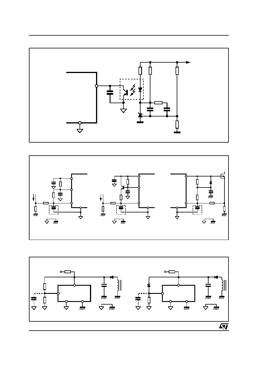
Figure 36. Typical E/A compensation networks.
L4990 - L4990A
19/24
L4990
COMP
D97IN508
TL431
V
OUT
VFB
6
5
Figure 37. Feedback with optocoupler
L4990
OPTIONAL
D97IN509A
I
V
REF
SGND
R
T
C
T
RCT
R
SLOPE
R
SENSE
ISEN
L4990
OPTIONAL
I
V
REF
SGND
R
T
C
T
RCT
R
SLOPE
R
SENSE
ISEN
L4990
OPTIONAL
OUT
SGND
R
R
R
SLOPE
R
SENSE
ISEN
C
SLOPE
4
2
13
12
4
2
13
12
13
12
10
Figure 38. Slope compensation techniques
Figure 39. Protection against overvoltage/feedbackdisconnection (latched)
L4990
D97IN510
SGND
DIS
V
CC
R
START
PGND
8
14
12
11
L4990
D98IN904
SGND
DIS
V
CC
R
START
PGND
8
14
12
11
V
Z
2.2K
L4990 - L4990A
20/24
L4990
D97IN511A
DC
V
CC
VREF
R
START
3
12
8
4
11
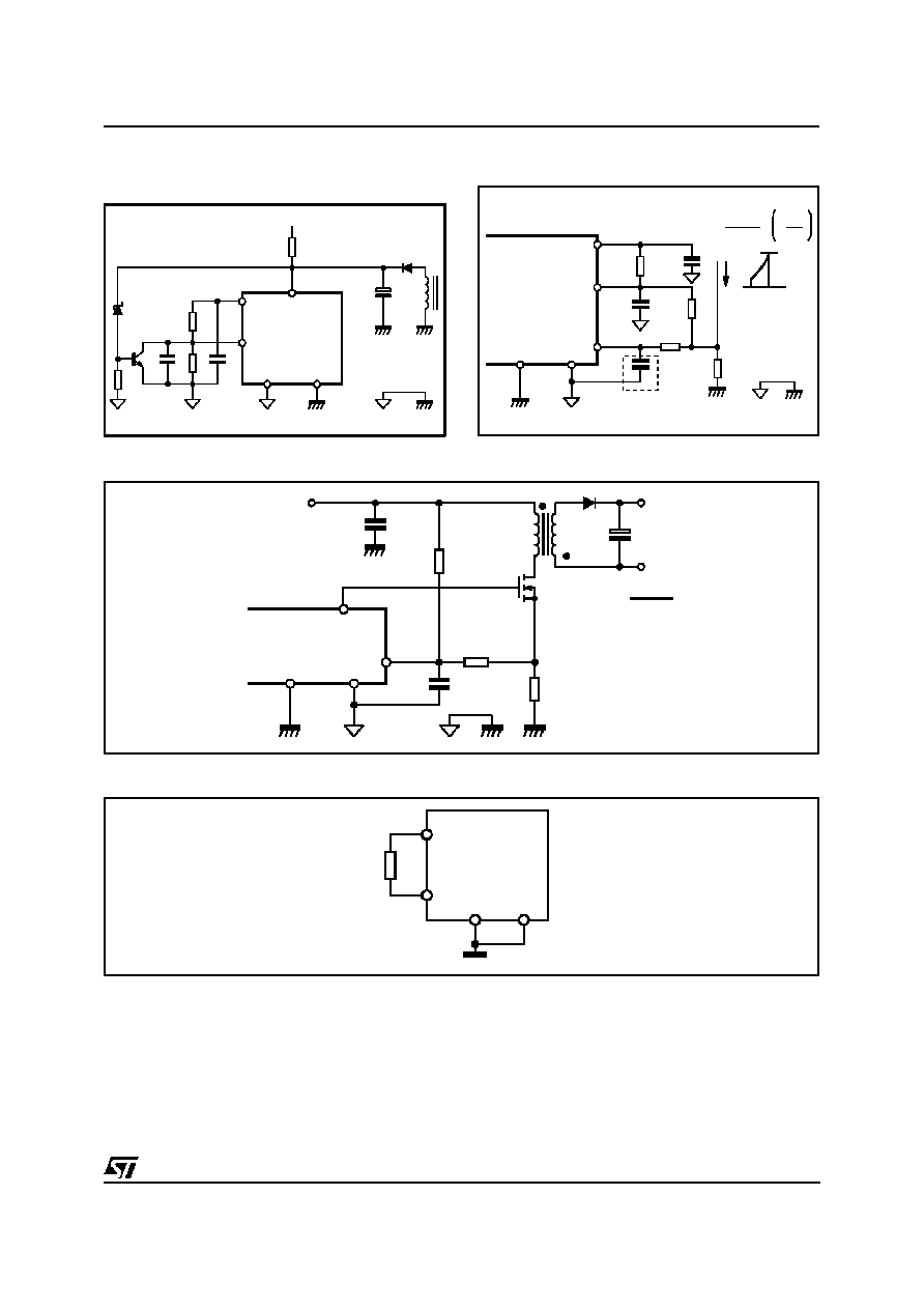
Figure 40. Protection against overvol-
tage/feedback disconnection (not
latched)
D97IN512A
PGND
L4990
OPTIONAL
VREF
SGND
DIS
ISEN
I
4
14
13
12
11
R
SENSE
R
2
R
1
I
pk
I
pk max
2.5
R
SENSE
1-
R
2
R
1
∑
Figure 41. Device shutdown on overcurrent
D97IN513
PGND
L4990
OUT
SGND
ISEN
Lp
R
FF
R
V
IN
R
FF
= 5∑10
6
R∑Lp
RSENSE
RSENSE
13
10
12
11
80
˜
400V
DC
Figure 42. Constant power in pulse-by-pulse current limitation (flyback discontinuous)
REFERENCES
[1] Efficient active Clamp for Off-line Applications using L4990 and L6380 (N.Tricomi, G. Gattavari,
C. Adragna, PCIM96 - NURBERG).
[2] 25W Off-Line Autoranging Battery Charger with L4990 (AN889)
[3] 300W Secondary Controlled Two-Switch Forward Converter with L4990 (AN890)
[4] SMPS with L4990 for Multisync Monitors (AN891)
[5] High performance VRM using L4990A, for Pentium Pro
Æ
processor (AN908).
L4990
DC
10K
COMP
3
6
12
13
SGND
ISEN
D97IN570A
Figure 43. Voltage mode operation.
L4990 - L4990A
21/24
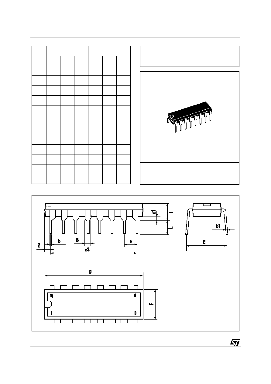
DIP16
DIM.
mm
inch
MIN.
TYP.
MAX.
MIN.
TYP.
MAX.
a1
0.51
0.020
B
0.77
1.65
0.030
0.065
b
0.5
0.020
b1
0.25
0.010
D
20
0.787
E
8.5
0.335
e
2.54
0.100
e3
17.78
0.700
F
7.1
0.280
I
5.1
0.201
L
3.3
0.130
Z
1.27
0.050
OUTLINE AND
MECHANICAL DATA
L4990 - L4990A
22/24
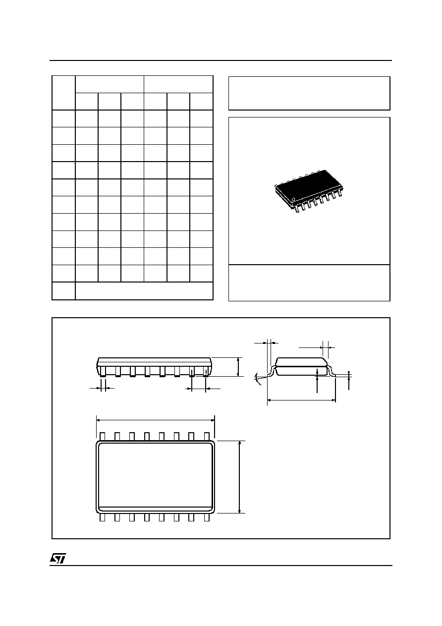
DIM.
mm
inch
MIN.
TYP.
MAX.
MIN.
TYP.
MAX.
A
2.35
2.65
0.093
0.104
A1
0.1
0.3
0.004
0.012
B
0.33
0.51
0.013
0.020
C
0.23
0.32
0.009
0.013
D
10.1
10.5
0.398
0.413
E
7.4
7.6
0.291
0.299
e
1.27
0.050
H
10
10.65
0.394
0.419
h
0.25
0.75
0.010
0.030
L
0.4
1.27
0.016
0.050
K
0
∞
(min.)8
∞
(max.)
h x 45
A
e
B
D
E
A1
H
L
C
K
16
1
8
9
SO16 Wide
OUTLINE AND
MECHANICAL DATA
L4990 - L4990A
23/24

Information furnished is believed to be accurate and reliable. However, STMicroelectronics assumes no responsibility for the consequences
of use of such information nor for any infringement of patents or other rights of third parti es which may result from its use. No license is
granted by implication or otherwise under any patent or patent rights of STMicroelectronics. Specification mentioned in this publication are
subject to change without notice. This publication supersedes and replaces all information previously supplied. STMicroelectronics products
are not authorized for use as critical components in life support devices or systems without express written approval of STMicroelectronics.
The ST logo is a registered trademark of STMicroelectronics
©
1999 STMicroelectronics ≠ Printed in Italy ≠ All Rights Reserved
STMicroelectronics GROUP OF COMPANIES
Australia - Brazil - China - Finland - France - Germany - Hong Kong - India - Italy - Japan - Malaysia - Malta - Morocco -
Singapore - Spain - Sweden - Switzerland - United Kingdom - U.S.A.
http://www.st.com
L4990 - L4990A
24/24