 | –≠–ª–µ–∫—Ç—Ä–æ–Ω–Ω—ã–π –∫–æ–º–ø–æ–Ω–µ–Ω—Ç: L5170 | –°–∫–∞—á–∞—Ç—å:  PDF PDF  ZIP ZIP |
L5170
OCTAL LINE DRIVER
ADVANCE DATA
OCTAL LINE DRIVER FOR:
≠ EIA STD: RS232D; RS423A
≠ CCIT: V.10; V.28
NO EXTERNAL COMPONENTS
VERY LONG TRANSMISSION LINE (5000ft)
50V EOS OUTPUT PROTECTION
DESCRIPTION
L5170 is an octal line driver unit in DIP28 and
PLCC28 packages intended for use in the EIA std
RS232D, RS423A and CCITT V.10 and V.28 ap-
plications.
With no external components L5170 is able to
drive a line up to 5000ft assuming the line capaci-
tance is 35pF per ft and the capacitance of the fil-
ter connectors/protection components add up to
the total capacitance load. The drivers typically
run in short circuit current mode whenever the ca-
ble attached is over 500ft.
This is advanced information on a new product now in development or undergoing evaluation. Details are subject to change without notice.
March 1993
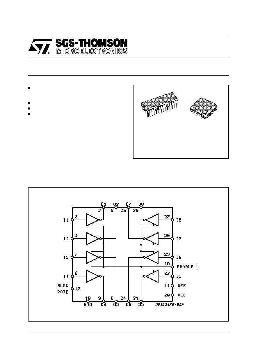
DIP28
PLCC28
ORDERING NUMBERS:
L5170A
L5170D
BLOCK DIAGRAM
1/9
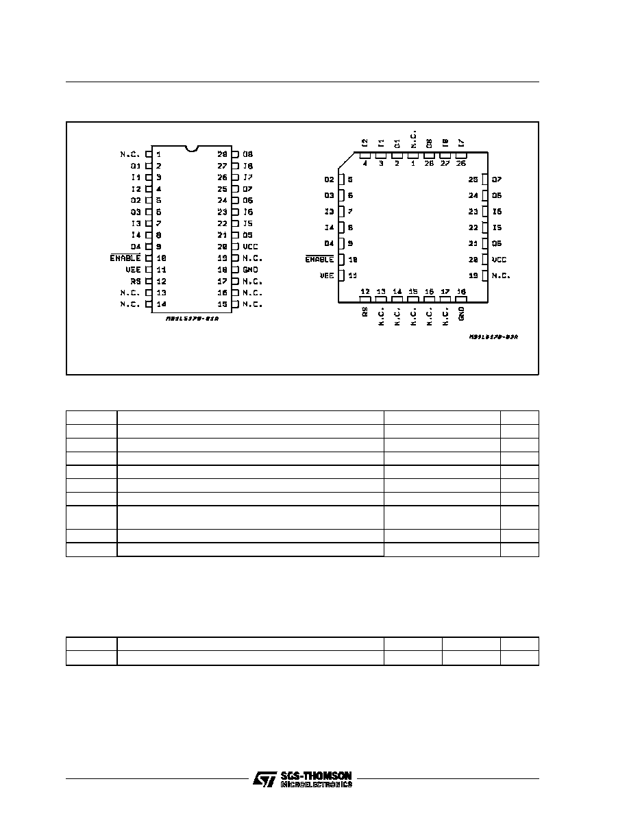
PIN CONNECTIONS (Top views)
DIP28
PLCC28
ABSOLUTE MAXIMUM RATINGS
Symbol
Parameter
Value
Unit
V
CC
Supply Voltage
+15
V
V
EE
Supply Voltage
≠ 15
V
V
i
Input Voltage (Enable Data)
≠ 1.5 to 7
V
V
O
Output Voltage
±
6
V
I
O
Output Current (**)
±
150
mA
SR
Minimum Slew Resistor (***)
1.5
1K
P
tot
Power Dissipation at T
amb
= 70
∞
C (PLCC28) (*)
(DIP28) (*)
1.2
1.3
W
W
T
op
Operating Free Air Temperature Range
0 to +70
∞
C
T
stg
Storage Temperature Range
-65 to 150
∞
C
Notes:
(*) Mounted on board with minimized dissipating copper area.
(**) Minimum Current per driver. Do not exceed maximum power dissipation if more than one input is on.
(***) Minimum value of the resistor used to set the slew rate.
THERMAL DATA
Symbol
Description
PLCC28
DIP28
Unit
R
th j-amb
Thermal Resistance Junction-ambient (*)
Max.
67
62
∞
C/W
L5170
2/9
AC ELECTRICAL CHARACTERISTICS (V
CC
= 9 to 11V; V
EE
= ≠ 9 to ≠ 11V T
amb
=0 to 70
∞
C, unless
otherwise specified
Symbol
Parameter
Test Condition
Min.
Typ.
Max.
Unit
V
OH
High Level Output Voltage
V
in
= 0.8V
R
L
= inf
R
L
= 3K
R
L
= 450
(see note 1)
5
5
4.5
6
6
6
V
V
V
V
OL
Low Level Output Voltage
V
in
= 2.4V
R
L
= inf
R
L
= 3K
R
L
= 450
(see note 1)
≠ 6
≠ 6
≠ 6
≠ 5
≠ 5
≠ 4.5
V
V
V
V
Ol
Output Voltage Balance
|V
CC
| = |V
EE
|; R
L
= 450
0.4
V
V
IH
High Level Input Voltage
2
V
V
IL
Low Level Input Voltage
0.8
V
V
IK
Input Clamp Voltage
I
IN
= ≠ 15mA
≠ 1.5
V
I
IH
High Level Input Current
V
IN
= 2.4V
40
µ
A
I
IL
Low Level Input Current
V
IN
= 0.4V
≠ 400
µ
A
I
CC
Positive Supply Current
V
IN
= 2.4V; R
S
= 2K
; R
L
= 3K
C
L
= 2.5nF; (See note 2)
30
mA
I
CC1
Positive Supply Current
V
IN
= 0.4V; R
S
= 2K
; R
L
= 3K
C
L
= 2.5nF; (See note 2)
40
mA
I
EE
Negative Supply Current
V
IN
= 2.4V; R
S
= 2K
; R
L
= 3K
C
L
= 2.5nF; (See note 2)
≠ 30
mA
I
EE1
Negative Supply Current
V
IN
= 0.4V; R
S
= 2K
; R
L
= 3K
C
L
= 2.5nF; (See note 2)
≠ 40
mA
I
sh
Output Short Circuit Current
V
O
= 0V; V
IN
= 2.4V; (see fig.1)
25
100
mA
I
sl
Output Short Circuit Current
V
O
= 0V; V
IN
= 2.4V; (see fig.1)
≠ 100
≠ 25
mA
I
bal
Output Current Balance
Ish/Isl = Ibal
0.625
1.6
mA/mA
I
x
Output Leakage Current
See fig.2,3 and note 3
V
O
= 6V
V
O
= ≠ 6V
≠ 70
70
µ
A
µ
A
t
r
Rise time (see note 4 and 5; see
figure 4A)
R
L
= 450
; C
L
= 50pF
R
slew
= 5.34K
±
1%
2
2.7
µ
s
t
rc1
R
L
= 450
; C
L
= 0.01
µ
F
R
slew
= 10K
±
1%
10
µ
s
t
rc2
R
L
= 450
; C
L
= 0.1
µ
F
R
slew
= 10K
±
1%
50
µ
s
t
rc3
R
L
= 450
; C
L
= 2.5nF
R
slew
= 2K
±
1%
0.65
1.2
µ
s
t
rc4
R
L
= 450
; C
L
= 2.5nF
R
slew
= 10K
±
1%
3.25
6
µ
s
t
f
Fall time (see note 4 and 5; see
figure 4A)
R
L
= 450
; C
L
= 50pF
R
slew
= 5.34K
±
1%
2
2.7
µ
s
t
fc1
R
L
= 450
; C
L
= 0.01
µ
F
R
slew
= 10K
±
1%
10
µ
s
t
fc2
R
L
= 450
; C
L
= 0.1
µ
F
R
slew
= 10K
±
1%
50
µ
s
t
fc3
R
L
= 450
; C
L
= 2.5nF
R
slew
= 2K
±
1%
0.65
1.2
µ
s
t
fc4
R
L
= 450
; C
L
= 2.5nF
R
slew
= 10K
±
1%
3.25
6
µ
s
Note 1: The Output under load must not drop below 90% of the open circuit drive level.
Note 2: This represents the static condition only. Applications can see 130mA normal current draw for clock and data lines with up to 500mA
transients when all lines are transitioning at the same time. Over 500ft of cable slew rate is governed by the drivers ability to sink current.
The currents are rougly equivalent to the short circuit current.
L5170
3/9
AC ELECTRICAL CHARACTERISTICS (continued)
Symbol
Parameter
Test Condition
Min.
Typ.
Max.
Unit
t
lz
Output Enable to Output
(see figure 4B)
R
L
= 450
; C
L
= 50pF
R
slew
= 10K
5
µ
s
t
nz
5
µ
s
t
zl
150
µ
s
t
zh
150
µ
s
t
plh
Propagation (see figure 4C)
R
L
= 450
; C
L
= 50pF
R
slew
= 2K
0.3
0.9
µ
s
t
ph1
0.3
0.9
µ
s
LINE TRANSIENT IMMUNITY (Considering the following cases: Powered ON, Powered OFF-Low im-
pedance power supply and Powered OFF-High impedance supply).
ESD
Elettrostatic Discharge
Tested per MIL-STD-883
(see note 6)
2
KV
EOS
Electrical Overstress
Transient pulse both polarities
for 100
µ
s (see note 7)
50
V
Note 3: The output leakage is measured under the following conditions:
a) The Driver tristated
b) Power supply OFF, and the power pins shorted to Ground
c) Power supply OFF. Impedances between power pins open and power pins shorted to Ground.
Note 4: The output waveform should not show any signs of oscillations under any load variation between o.1VVss and 0.9Vss. The oscillation
allowed when V
SS
< 0.1V
SS
and V
ss
>0.9V
ss
shall be 10% of V
ss
.
Note 5: t
fc1
thru t
rc4
shall be within
±
20% of t
rc1
thru t
r c4
respectively.
Note 6: All pins are required to withstand parameter.
Note 7: Output pins are required to withstand fig.5 without any degradation to the circuit.
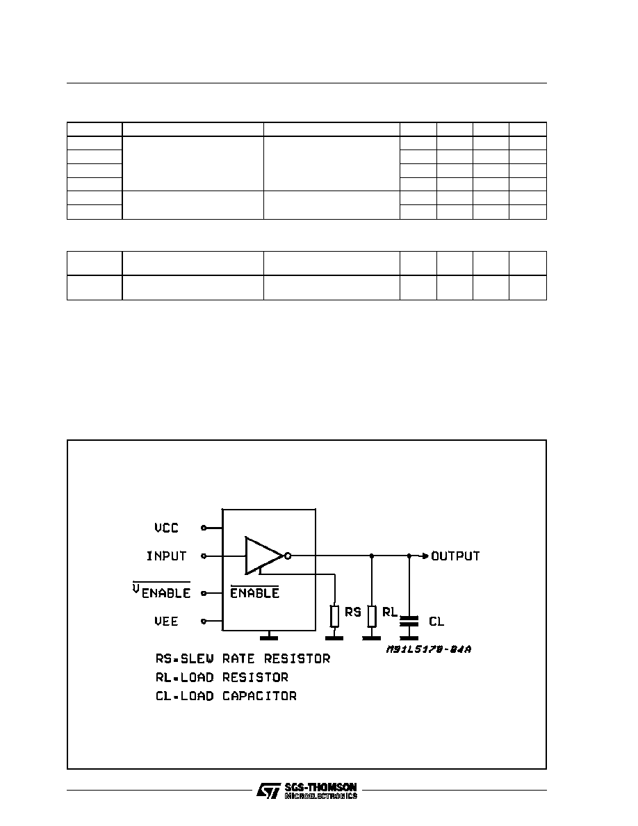
TEST CIRCUIT
L5170
4/9
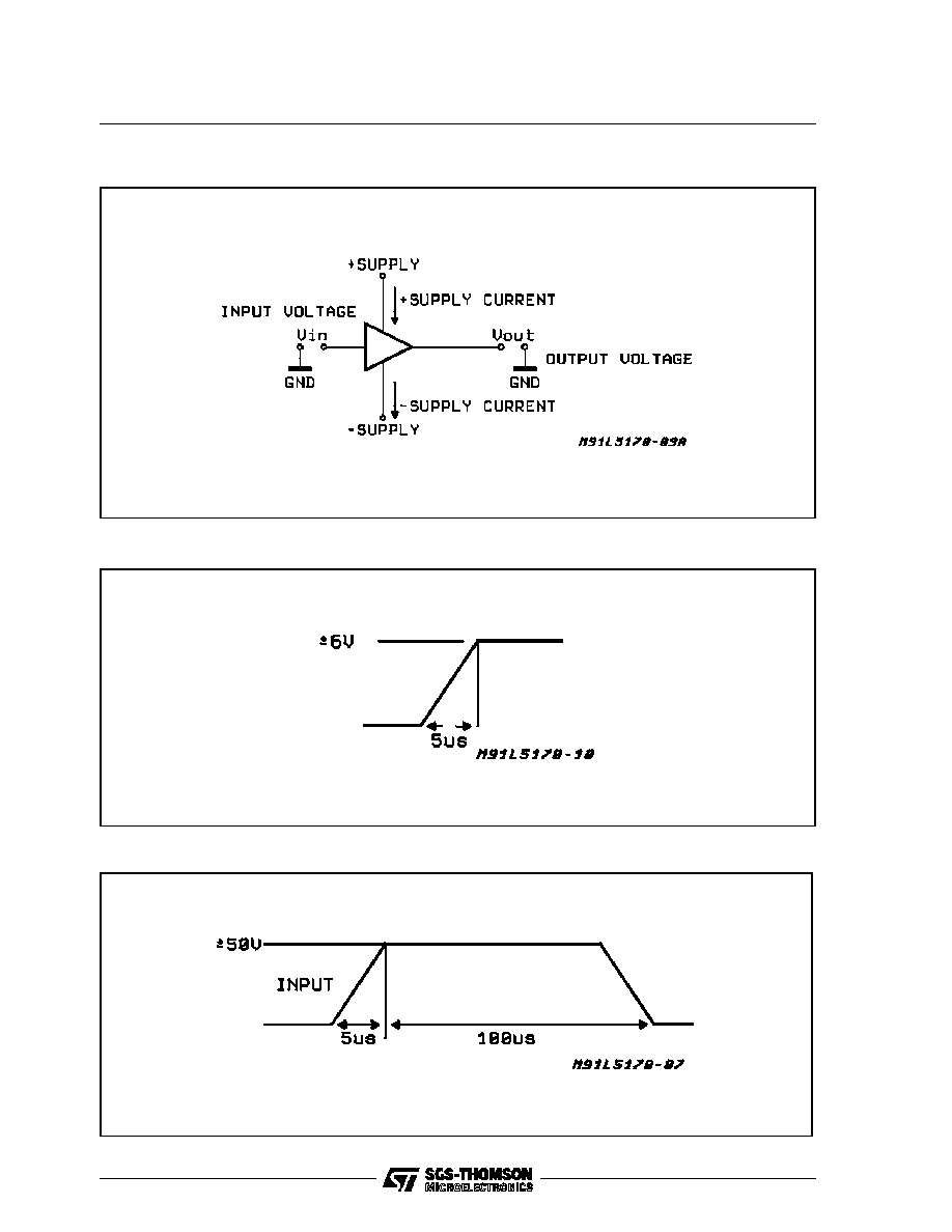
Figure 1: Output Leakage Test Circuit
Figure 2: Output Voltage Rise Time
Figure 3: EOS Requirements
L5170
5/9
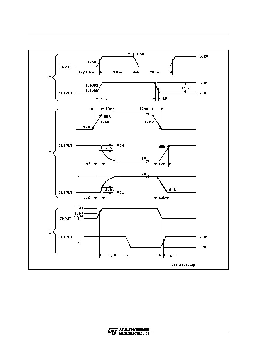
Figure 4: Waveforms
L5170
6/9
DIP28 PACKAGE MECHANICAL DATA
DIM.
mm
inch
MIN.
TYP.
MAX.
MIN.
TYP.
MAX.
a1
0.63
0.025
b
0.45
0.018
b1
0.23
0.31
0.009
0.012
b2
1.27
0.050
D
37.34
1.470
E
15.2
16.68
0.598
0.657
e
2.54
0.100
e3
33.02
1.300
F
14.1
0.555
I
4.445
0.175
L
3.3
0.130
L5170
7/9
PLCC28 PACKAGE MECHANICAL DATA
DIM.
mm
inch
MIN.
TYP.
MAX.
MIN.
TYP.
MAX.
A
12.32
12.57
0.485
0.495
B
11.43
11.58
0.450
0.456
D
4.2
4.57
0.165
0.180
D1
2.29
3.04
0.090
0.120
D2
0.51
0.020
E
9.91
10.92
0.390
0.430
e
1.27
0.050
e3
7.62
0.300
F
0.46
0.018
F1
0.71
0.028
G
0.101
0.004
M
1.24
0.049
M1
1.143
0.045
L5170
8/9

Information furnished is believed to be accurate and reliable. However, SGS-THOMSON Microelectronics assumes no responsibility for the
consequences of use of such information nor for any infringement of patents or other rights of third parties which may result from its use. No
license is granted by implication or otherwise under any patent or patent rights of SGS-THOMSON Microelectronics. Specifications men-
tioned in this publication are subject to change without notice. This publication supersedes and replaces all information previously supplied.
SGS-THOMSON Microelectronics products are not authorized for use as critical components in life support devices or systems without ex-
press written approval of SGS-THOMSON Microelectronics.
©
1995 SGS-THOMSON Microelectronics - All Rights Reserved
SGS-THOMSON Microelectronics GROUP OF COMPANIES
Australia - Brazil - France - Germany - Hong Kong - Italy - Japan - Korea - Malaysia - Malta - Morocco - The Netherlands - Singapore -
Spain - Sweden - Switzerland - Taiwan - Thaliand - United Kingdom - U.S.A.
L5170
9/9