 | –≠–ª–µ–∫—Ç—Ä–æ–Ω–Ω—ã–π –∫–æ–º–ø–æ–Ω–µ–Ω—Ç: L584 | –°–∫–∞—á–∞—Ç—å:  PDF PDF  ZIP ZIP |
L584
November 1988
MULTIFUNCTION INJECTION INTERFACE
PRELI MINARY DATA
.
DRIVES ONE OR TWO EXTERNAL DAR-
LINGTONS
.
DUAL AND SINGLE LEVEL CURRENT CON-
TROL
.
SWITCHMODE CURRENT REGULATION
.
ADJUSTABLE HIGH LEVEL CURRENT DURA-
TION
.
WIDE SUPPLY RANGE (4.75 - 46V)
.
TTL-COMPATIBLE LOGIC INPUTS
.
THERMAL PROTECTION
.
DUMP PROTECTION
DESCRIPTION
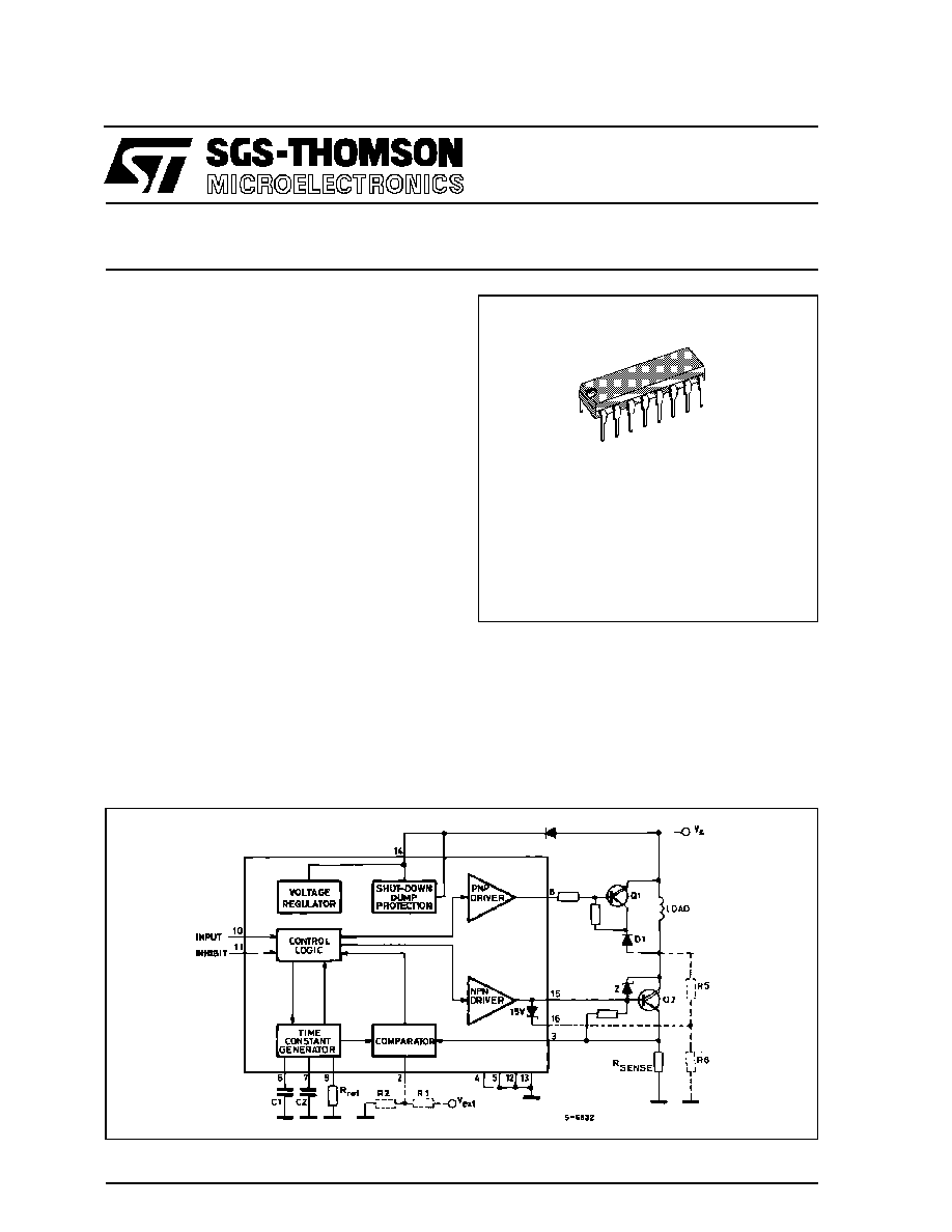
The L584 is designed to drive injector solenoids in
electronic fuel injection systems and generally in-
ductive loads for automotive applications. The de-
vice is controlled by two logic inputs and features
switchmode regulation of the load current driving an
external darlington and an auxiliary one for the cur-
rent recirculation. A key feature of the L584 is flexi-
bility. It can be used with a variety of darlingtons to
match the requirements of the load and it allows
both simple and two level current control. Moreover,
DIP1 6 (12 + 2 + 2)
ORDERING NUMBER : L584
the drive waveshape can be adjusted by external
components. Other features of the device include
dump protection, thermal shutdown, a supply vol-
tage range of 4.75 - 46V and TTL-compatible inputs.
The L584 is suppliedin a 16 lead Powerdip package
which uses the four center pins to conduct heat to
the PC board copper.
BLOCK DIAGRAM
1/13
THERMAL DATA
Symbol
Parameter
Value
Unit
R
th j-pins
Thermal Resistance Junction-pins
Max.
15
∞
C/W
R
th j-amb
Thermal Resistance Junction-ambient
Max.
80
∞
C/W
ABSOLUTE MAXIMUM RATINGS
Symbol
Parameter
Value
V
S
DC Supply Voltage (pin 1 open)
Positive Transient Voltage
(pin 1 connected to V
S
,
f
fall time constant = 100ms)
(5ms
t
rise
10ms, R
source
0.5
)
≠ 0.2V min; +50V Max
+60V Max
V
1
Input Voltage (pins 10, 11)
≠ 0.2V min; +7V Max
V
r
External Reference Voltage (pin 2)
≠ 0.2V min; +7V Max
V
sens
Sense Voltage (pin 3)
≠ 0.2V min; +7V Max
V
8
Max D.C. and Transient Voltage
50V
I
r
Reference Current (pin 9)
5mA Max
Tstg, Tj
Storage and Junction Temperature Range
≠55 to 150
∞
C
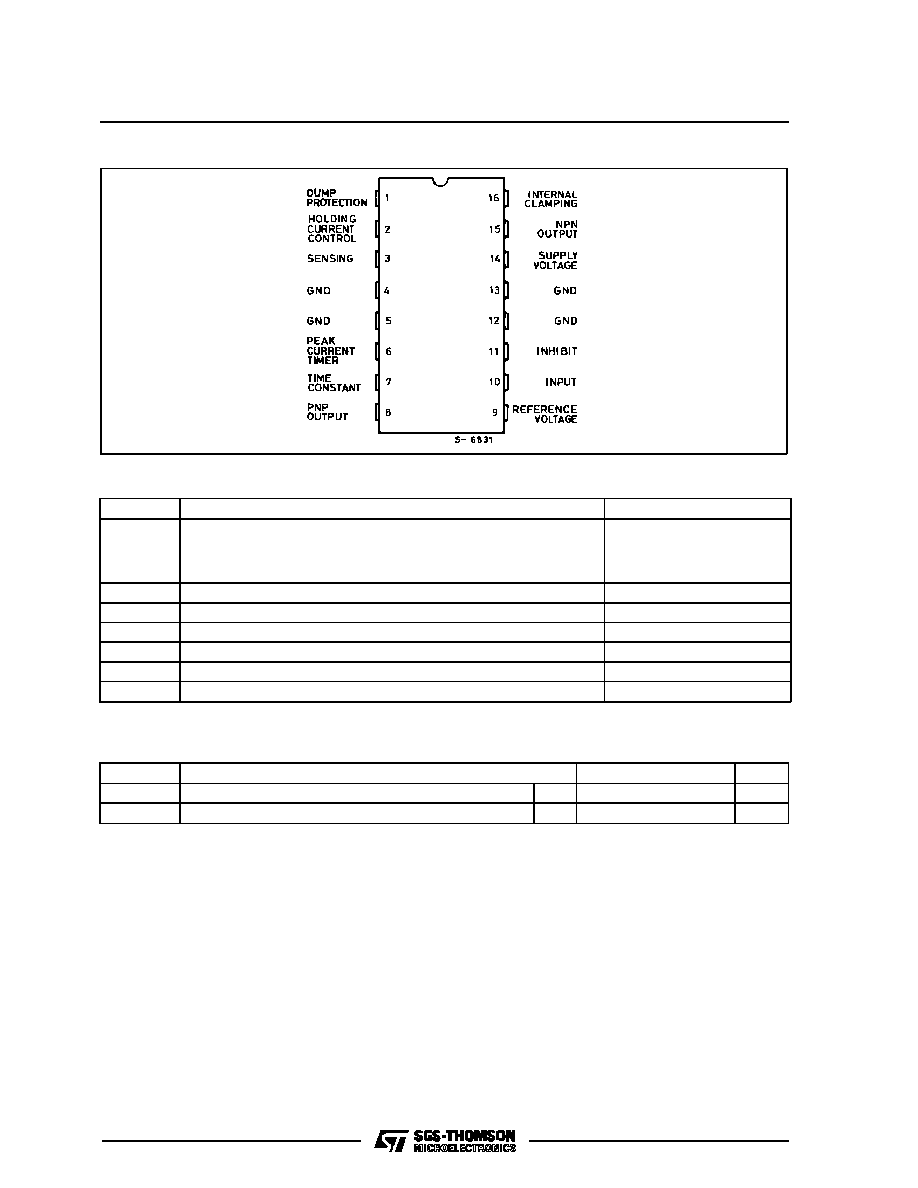
PIN CONNECTION
* Obtained with the GND pins soldered to printed circuit with minimized copper area.
L584
2/13

PIN FUNCTIONS
N
o
Name
Functions
1
Dump Protection
With pin 1 connected to pin 14 the device is protected against dump voltage
60V.
The protectio.n operates at V
S
32V (typ.). If this protection is not used the pin must
be left open
2
Holding Current Control
The voltage V
set
applied to this pin sets the holding current level.
3
Sensing
Connection for load current sense resistor. Vazlue sets the peak and holding current
levels. I
P
= 0.45/R
S
(typ.); I
h
= V
set
/R
s
. (see block diagram and fig. 4).
4
Ground
Ground Connection. With pins 5, 12 and 13 conducts heat to pc board copper.
5
Ground
See pin 4.
6
Peak Current Timer
A capacitor connected between this pin and ground sets the duration of the high level
current (t
2
in fig. 4)
7
Discharge Time Constant A capacitor connected between this pin and ground sets the duration of t
off
(fig. 4). If
grounded, the current switchmode control is suppressed.
8
PNP Driving Output
Current sink for external PNP darlington (for recirculation). I
dp
= 35 Ir (typ).
9
Reference Voltage
A resistor connected between this pin and ground sets the internal current reference,
I
r
. The recommended value is 1.2k
giving Ir = 1mA (typ.).
10
Input
TTL-compatible Input. A high level on this pin activates the output, driving the load.
11
Inhibit
TTL-compatible Inhibit Input. A high level on this input disables the output stages and
logic circutry, irrespective of the state of pin 10.
12, 13
Ground
See Pin 4.
14
Supply Voltage
Supply Voltage Input.
15
NPN Driving Output
Current Source for External NPN Darlington (load driver).I
dn
= 100 I
r
(typ.)
16
Internal Clamping
Internal Clamp Zener for Fast Turn-off.
000
L584
3/13

ELECTRICAL CHARACTERISTICS (V
s
(Pin 14) = 14.4V; ≠40
Tj
105
∞
C; R
ref
= 1.20K
unless
otherwise specified; refer to fig. 1)
Symbol
Parameter
Test Condiction
Min.
Typ.
Max.
Unit
V
S
Operating Supply Voltage
Pin 1 Open
4.75
44
V
V
d
Dump Protection Threshold
Pin 1 = V
S
28
36
V
R
d
Dump Protection Input Resistance
Pin 1 to GND
18
50
k
I
q
Quiescent Current
Pin 14
45
mA
V
i
Input Threshold Voltages
Pin 10, 11
Low
High
2.0
0.8
V
V
I
i
Input Current
Pin 10, 11
Low
High
≠100
≠250
µ
A
µ
A
V
r
Reference Voltage
Pin 9
1.15
1.35
V
R
r
Reference Resistor Range
Pin 9 to GND
I
r
= V
r
/R
r
1
3.3
k
I
6
Peak Duration Control Current
Pin 6
V
pin 6
1.8V
I
r
/9.50
|
I
r
/6.00
|
A
V
6th
Peak Duration Control
Comparator Threshold
Pin 6
1.20
1.6
V
V
6SAT
Pin 6 Saturation Voltage
Pin 6
(discharge state)
200
mV
I
7
Off Duration Control Current
Pin 7
V
pin 7
1.8V
(I
r min
)/9.50 | (I
r max
)/6.00
|
A
V
7th
Off Duration Control
Comparator Threshold
Pin 7
1.20
1.6
V
V
7SAT
Pin 7 Saturation Voltage
Pin 7
(discharge state)
200
mV
V
spt
Peak Current Threshold Voltage
Pin 3
400
500
mV
V
set
Holding Current Set Voltage Range Pin 2
0
2
V
V
set
Holding Current Set Voltage Range Pin 3, Peak Value, dV/dt
1V/
s
V
set
≠
0.01
V
set
+
0.01
V
I
3
Pin 3 Bias Current
V
pin 3
= 600mV
≠200
µ
A
V
cl
Recirculation
Zener
Clamping
Voltage
Pin 16 to Pin 15 @ 200mA into Pin16
13.5
18.5
V
I
dn
NPN Driver Source Current
V
pin 15
= 0V
70 x I
r
|
140 x I
r
A
I
dp
PNP Driver Sink Current
Vpin 8
4.75V
25 x I
r
|
60 x I
r
A
L584
4/13

Figure 1 : Components Connected to Pins 6 and 7 Determine the Load Current Waveshape.
COMPONENTS ON PINS 6 AND 7
LOAD CURRENT WAVEFORM
APPLICATION INFORMATION
Controlled by a logic input and an inhibit input (both
TTL compatible), the device drives the external dar-
lington(s) to produce a load current waveform as
shown in figure 4. This basic waveform shows that
the device produces an initial high level current in or-
der to ensure a fast opening, followed by a holding
level current as long as the input is active. Both
the peak and holding current are regulated by the
L584's switchmode circuitry.
The duration of the high level current and the values
of the peak and the holding currents can be adjusted
by external components.
Moreover, by omitting C1, C2 or both it is possible
to realize single-level current control, a transitory
peak followed by a regulated holding current or a
simple peak (figure 1).
The peak and holding current values are always re-
L584
5/13
ferred, in the following formula, to I
E
, emitter current
of the external darlington Q2,
I
E
= I
LOAD
+ I
dn
because the sensing detection is on the darlington
emitter (not directly on the load).
The peak current level I
p
, is set by the sensing re-
sistor, R
s
, and is found from :
I
p
= 0.45 / R
s
(typ)
The peak value of holding current level, I
h
, is set by
a voltage (V
set
) applied to pin 2, giving :
I
hp
= V
setth
/ R
s
= (V
set
±
10mV)/R
s
The peak to hold current ratio is fixed by V
set
:
I
p
/ I
hp
= 0.45 / V
setth
V
set
is fixed by an external reference and a voltage
divider (V
ext
, R1, R2 in fig 2) :
V
set
= V
ext
* R2 / (R1 + R2)
Due to the particular darlington storage time and the
device reaction time not very significant differences
can be found between I
p
and I
h
values based on the
previous formula and the real values seen in the ap-
plications.
If the holding current function is not used, pin 2 can-
not be left floatingand it must be connectedto GND.
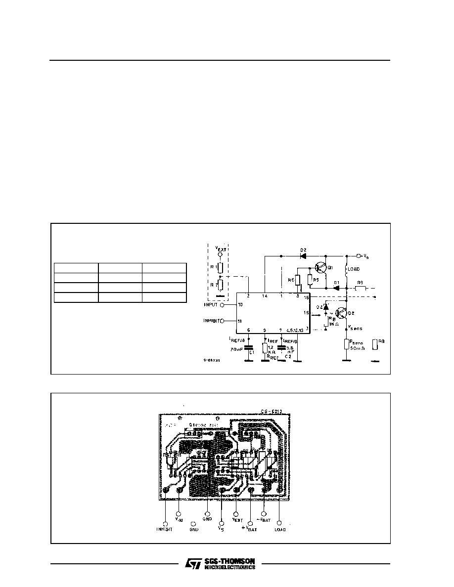
Figure 2 : Application Circuit Showing the Optional Components. In particular it illustrates how the holding
current level is adjusted independentlyof the peak current (with R1, R2, V
ext
) and how the internal
zener clamp is connected. This circuit produces the waveforms shown in Fig. 4.
I
o
(A)
Q1
Q2
4
BDX54
BDX53
8
BDW94
BDW93
12
BDV64
BDV65
Figure 3 : P.C. Board and Components Layout of the Circuit of Fig. 2 (1 : 1 scale).
L584
6/13

The drive current for the two darlingtons and the
waveform time constants are all defined in turn by a
resistor between pin 9 and ground.
The recommended value for I
r
is 1mA which is ob-
tained with a 1.2K
resistor. The darlington drive
currents are given by :
PNP : I
dp
= 35 I
r
typ.
NPN : I
dn
= 100 I
r
typ.
The duration of the high current level (t
2
in fig 4) is
set by a capacitor connected between pin 6 and
ground. This capacitor, C1 is related to the duration,
t
2
, by :
V
6th
≠ V
6sat
C
1
t
2
= C
1
= 12
(typ.)
I
6
I
ref
The discharge time constant (t
off
in fig 4) is set by a
capacitor C
2
between pin 7 and ground and is found
from :
V
7th
≠ V
7sat
C
r
t
off
= C2
= 12
(typ)
I
7
I
ref
Figure 4 : Waveforms of the Typical Application Circuit of Fig. 2.
L584
7/13

Figure 6 : In this application circuit, pin 6 is left open to give a single peak followed by a regulated holding
current.
Figure 5 : When pin 6 is grounded, as shown here, the injector current is regulated at a single level.
I
o
(A)
Q1
Q2
4
BDX54
BDX53
8
BDW94
BDW93
10
BDV64
BDV65
I
o
(A)
Q1
Q2
4
BDX54
BDX53
8
BDW94
BDW93
10
BDV64
BDV65
L584
8/13

Figure 7 : Switchmode control of the current can be suppressed entirely by leaving pin 6 open and
grounding pin 7. the peak current is still controlled.
Figure 8 : Applications circuit using only one darlington with a single level of the injector current.
I
o
(A)
Q1
Q2
4
BDX54
BDX53
8
BDW94
BDW93
10
BDV64
BDV65
L584
9/13

To have a very short off time when the L584 input
goes LOW, an internal zener is available on pin 16.
This zener is used with an external divider, R8, R9,
as shown in figure 2. Suitable values can be found
from :
V
pin 16
15V + V
BEQ2
+ VRsense
R9 + R8
V
CQ2
V
pin 16
.
R8
(V
CQ2
is the voltage at the collector of Q2. V
CQ2
max
is 47V if the pin 8 is used for slow recirculation as in
fig. 2).
To ensure stability, a small capacitor (about 200pF)
must be connected between the base and collector
of Q2 when pin 16 is used.
A different opportunityfor a fast off time is based on
the use of the external zener diode Dz. In this case
also the maximum Dz voltage value is 47V.
LOAD DUMP PROTECTION
To protect the device against the positive load dump
it is necessary to connect pin 1 to V
S
. In this case,
if V
S
is higher than 32V, the device turns off Q
2
and
turns on Q
1
. The external resistor R
6
must be used
(see application circuit) to avoid that pin 8 voltage
exceeds 50V during load dump. R
6
must be :
V
DUMP
≠ V
8
R
6
>
I
dp
where V
DUMP
is the dump voltage value and V
8
:
4.75V < V
8
< 47V.
For this R
6
value, the minimum supply voltage V
Smin
guaranteeing Q1 operation is given by :
V
Smin
=
R6
Ip
B
Q1
(+
2
)
V
BEQ1
R
5
+
V
8sat
In relation to V
Smin
it is no more verified I
dp
= 35 I
ref
(typ) even if the system correct operation is com-
pletely guaranteed.
The L584 application circuit suggested in these
notes allows the use of inductive loads with the low-
est possible series resistance (compatible with con-
structional requirements) and therefore reduces no-
tably the power dissipation.
For example, an electronic injector driven from
14.4V which draws 2.4A has a series resistance of
6
and dissipates 34.56W. Using this circuit a injec-
tor with a 1
series resistance can be used and the
power dissipation is :
P
d
= R
L
I
L
2
+ V
D
I
L
(1 ≠
) + V
sat
IL
+ R
S
I
L
2
where R
L
= resistance of injector = 1
V
D
= drop across diode, V
D
1V
V
sat
= saturation voltage of Q2,
1V
R
S
= R11 = 185m
= duty cycle = 20%
therefore :
Pd
5.76 + 1.92 + 0.48 + 0.21 = 8.37W
This given two advantages : the size (and cost) of
the injector is reduced and the drive current is re-
duced from 2.4A to about 0.4A.
The applicationcircuit of figure 9 is very similar to fig-
ure 2 except that it shows the use of two supplies :
one for the control circuit, one for the power stage.
L584
10/13

Figure 9 : Application circuit showing how two separate supplies can be used.
In this application it is assumed that the 5V supply
for L584 is taken from a logic supply, which is al-
ready protected, against load dump transients and
vol-tage reversal.
Pin 1 must be left open, as shown in fig. 9, if V
S
is
always lower than 46V even during the voltage tran-
sients.
Note that t
off
is also related to the required current
ripple
I on the peak or on the holding current level
by :
(I
o
≠
I) R
L
+ V
off
t
off
= ≠
ln
I
o
R
L
+ V
off
Where : Io is the initial current valuein OFF condition
(equal to Ip or IH in accordance to the current level
considered),
V
OFF
= V
DIODE
+ V
CEQ1
R
L
is the series resistance value of the induc-
tance L :
Therefore C
2
can be dimensioned directly by :
I
REF
L
ln
(I
o
≠
I) R
L
+ V
OFF
C
2
=
12
R
L
I
o
R
L
+ V
OFF
Note that t
off
is the same for both the peak and hold-
ing current.
t
on
time is given by :
L
V
on
≠ R(I1 ≠
I)
t
on
=
ln
R
V
on
≠ RI1
where : I1 is the final current value in ON condition
(equal to I
p
or I
H
in accordance to the current level
considered),
R = R
L
+ R
SENSE
V
on
= V
S
≠ V
CE
satQ2
If the constant times are respectively
L
L
> 20 t
off
and
> 20 t
on
R
R
it is possible to consider a purely inductive load and
therefore :
I
I
t
off
= L
; t
on
= L
V
o
V
on
L
R
L584
11/13
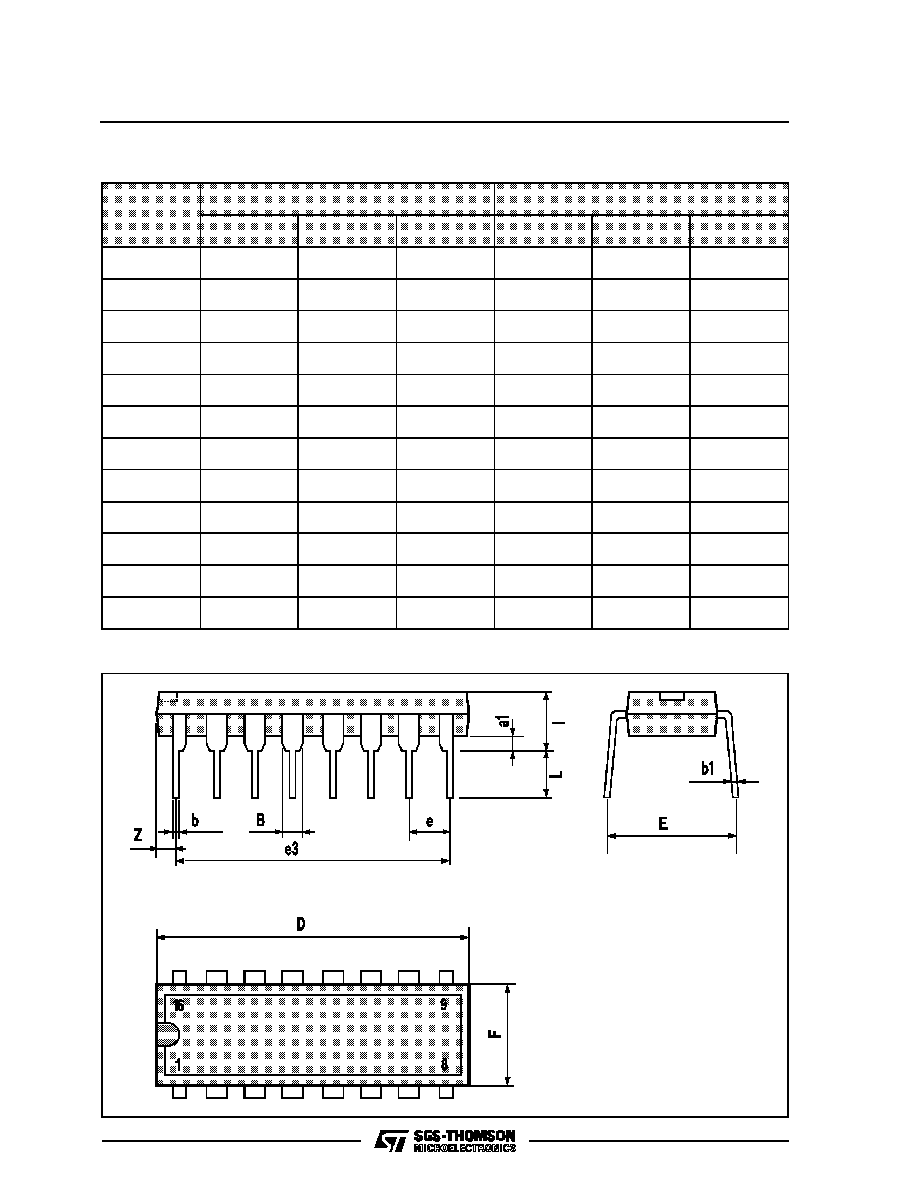
DIP16 PACKAGE MECHANICAL DATA
DIM.
mm
inch
MIN.
TYP.
MAX.
MIN.
TYP.
MAX.
a1
0.51
0.020
B
0.77
1.65
0.030
0.065
b
0.5
0.020
b1
0.25
0.010
D
20
0.787
E
8.5
0.335
e
2.54
0.100
e3
17.78
0.700
F
7.1
0.280
I
5.1
0.201
L
3.3
0.130
Z
1.27
0.050
L584
12/13

Information furnished is believed to be accurate and reliable. However, SGS-THOMSON Microelectronics assumes no responsibility for
the consequences of use of such information nor for any infringement of patents or other rights of third parties which may result from its
use. No license is granted by implication or otherwise under any patent or patent rights of SGS-THOMSON Microelectronics. Specifica-
tions mentioned in this publication are subject to change without notice. This publication supersedes and replaces all information pre-
viously supplied. SGS-THOMSON Microelectronics products are not authorized for use as critical components in life support devices or
systems without express written approval of SGS-THOMSON Microelectronics.
©
1994 SGS-THOMSON Microelectronics - All Rights Reserved
SGS-THOMSON Microelectronics GROUP OF COMPANIES
Australia - Brazil - France - Germany - Hong Kong - Italy - Japan - Korea - Malaysia - Malta - Morocco - The Netherlands - Singapore -
Spain - Sweden - Switzerland - Taiwan - Thaliand - United Kingdom - U.S.A.
L584
13/13