 | –≠–ª–µ–∫—Ç—Ä–æ–Ω–Ω—ã–π –∫–æ–º–ø–æ–Ω–µ–Ω—Ç: L585 | –°–∫–∞—á–∞—Ç—å:  PDF PDF  ZIP ZIP |
L585
November 1991
CAR ALTERNATOR REGULATOR
.
ALTERNATOR VOLTAGE CONTROL
.
COMPLETE FAULT DIAGNOSTICS
.
DRIVES 3 W LAMP DIRECTLY
.
LAMP SHORT CIRCUIT PROTECTION
.
SENSING INTERRUPT PROTECTION
.
100 V DUMP PROTECTION
.
300 V LOW ENERGY SPIKE PROTECTION
.
THERMAL PROTECTION
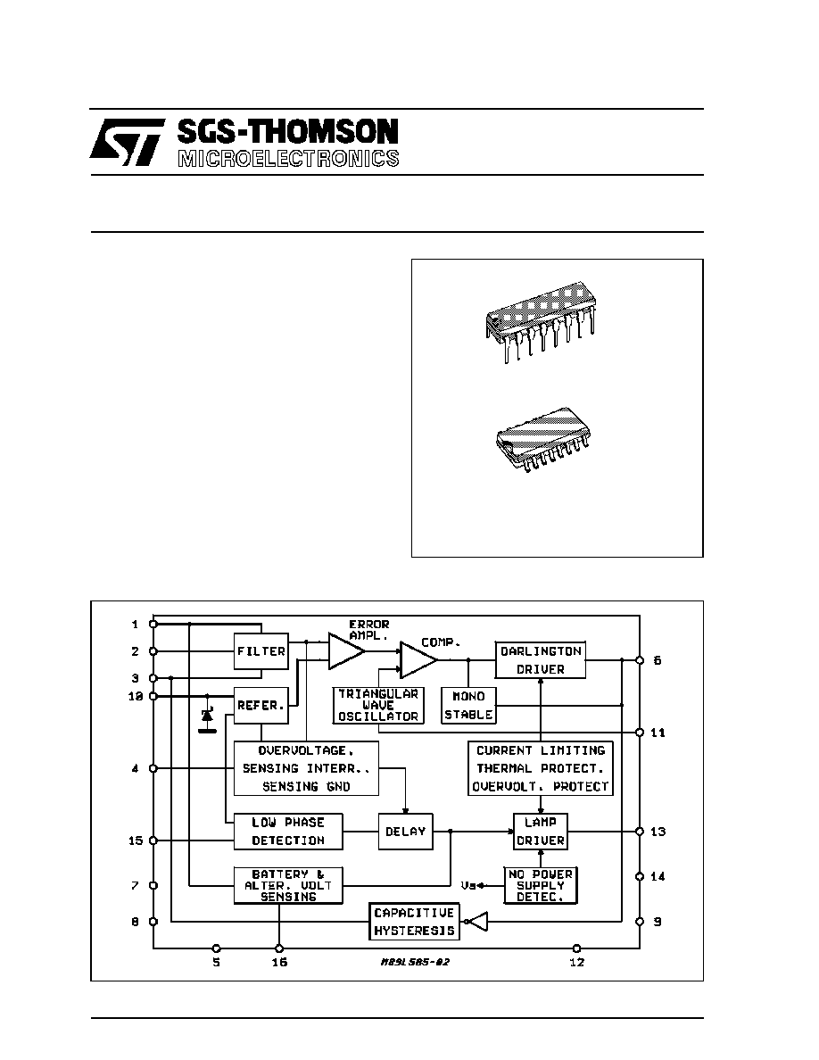
DESCRIPTION
The L585 is an integrated circuit designed for use
with an NPN darlington as a voltage regulator in a
threephase alternator charging system. It includes
fault diagnostic circuitry which drives a 3 W warning
lamp in fault conditions such as open or short circuit
connections. Protection against load dump tran-
sients, short circuits and low energy spikes is incor-
porated.
BLOCK DIAGRAM
DIP16
ORDERING NUMBERS : L585 (DIP16)
L585D1 (SO16)
SO16
1/9
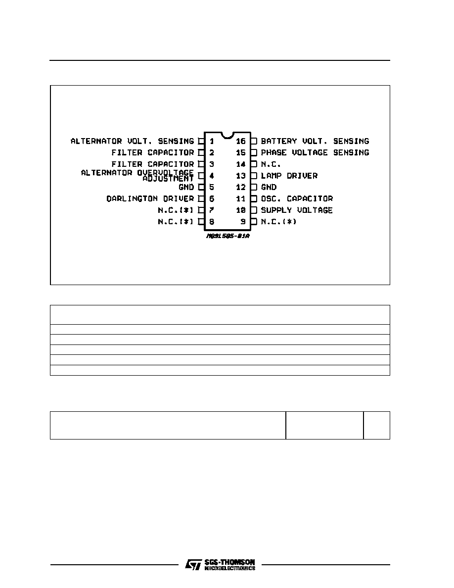
PIN CONNECTION
THERMAL DATA
Symbol
Parameter
Value
Unit
R
th j-amb
R
th j-alumina
(*)
Thermal Resistance Junction-ambient (*) for DIP 16
Thermal Resistance Junction-alumina for SO-16
Max
Max
80
50
∞
C/W
∞
C/W
ABSOLUTE MAXIMUM RATINGS
Symbol
Parameter
Value
Unit
V
S
Operating supply Voltage (through R
S
)
28
V
V
D
Dump Voltage
100
V
T
j
Junction Temperature Range
≠ 40 to 150
∞
C
P
tot
Power Dissipation at T
amb
= 80
∞
C
1
W
T
stg
Junction and Storage Temperature Range
≠ 55 to 150
∞
C
T
op
Operating Temperature Range
≠ 40 to 125
∞
C
No te : Soldered on PC board that simulates an application with medium device density on board.
(*) Thermal resistance junction-pins with the chip soldered on the middle of an alumina supporting substrate measuring 15 ˆ 20 mm ; 0.65 mm
thickness and infinite heathsink.
(*) MUST BE LEFT FLOATING
L585
2/9

PIN FUNCTIONS
N
∞
Name
Functions
1
Alternator Voltage
Sensing
Connection for voltage regulation sensing. The regulation sensitivity is a
function of R1 and is given by :
S =
VA
R1
=
0.5mV
/
2-3
Filter Capacitor
A capacitor connected between these two pins filters the feedback signal from
the regulated output. Typically the input impedance is 15K
.
4
Alternator Overvoltage
Adjustment
When this pin is left open circuit the overvoltage threshold is a described in the
specification. Typically the warning lamp is switched on when the voltage at
this pin is greater than 3.5V. This threshold can be modified with a resistor
between either the ground or pin 2.
5
GND
This pin must be connected to ground.
6
Darlington Driver
This pin drives the external darlington disabling it by shorting the current in R
B
to ground.
7-8-9
N.C.
These pins must be left floating.
10
IC Supply Voltage
Supply Voltage Input
A 7.5V (typical) Zener is present at the input.
11
Oscillator Capacitor
A capacitor connected to ground sets the frequency of the internal oscillator.
The frequency is given by :
fosc =
20 x 10
-
6
8.4
x
C
osc
12
GND
This pin must be connected to ground.
13
Lamp Driver
Current Driver for External Lamp for Diagnostics.
Internally protected agains short circuits (current limiting), load dump transients
and, by means of a zener, against low energy spikes.
14
NC
Not connected.
15
Phase Voltage Sensing.
Connection for no charge sensing from the alternator .
The internal low threshold is typically 2.4V. By means of the external divider
R3/R4 the threshold can be adjusted to give the required sensitivity.
16
Battery Voltage Sensing
Connection for Voltage Battery Sensing
This pin senses a failure of the alternator-battery lead as the voltage difference
V
A
-V
S
. The external resistor R2 limits the current in overvoltage protection.
L585
3/9

ELECTRICAL CHARACTERISTICS (V
s
= 14.4V ; ≠ 30
∞
C
T
j
100
∞
C unless otherwise specified ; refer to
application circuit)
Symbol
Parameter
Test Conditions
Min.
Typ.
Max.
Unit
REGULATION
V
S
Operating Supply Voltage
6
25
V
I
d
Quiescent Drain Current (pin 10)
V
10
= 5.5V
24
mA
V
A
Alternator Reg. Voltage
T
j
= 20
∞
C, t = 100ms
R
1
= 1.3K
(1)
T
j
= ≠ 30
∞
C
T
j
= + 100
∞
C
14.26
14.60
13.32
14.55
14.84
15.50
14.17
V
V
V
V
A
Voltage Reg. Range
10% < d < 90%
±
60
mV
S
Sensitivity to R
1
Variation
S = dV
A
/dR
1
0.35
0.65
mV/
TC
nS
Normalized S
Temperature Coeff.
1/S* dS/dT
≠ 2000
ppm/
∞
C
V
6 sat
Darlington Driver Satur. Voltage
I
6
= 20mA
200
mV
f
s
Oscillation Frequency
C
osc
= 20nF
80
170
Hz
I
1
Standby Current (pin 1)
V
batt
= 12V
2
mA
DIAGNOSTIC
V
AH
Overcharging Voltage
Threshold (2)
T
j
= 25
∞
C
R
1
= 1.3K
V
S
= V
AH
(3)
≠ 30
∞
C < T
j
< + 100
∞
C
1.054V
A
1.049V
A
1.086V
A
1.091V
A
V
V
V
PL
Low Level Phase Voltage
Threshold (no load) (4)
f = 600Hz, T
j
= 25
∞
C
≠ 30
∞
C < T
j
< + 100
∞
C
5
4.5
6
6
7
7.5
V
V
V
AS
Difference
Between
Altern.
and
Supply Voltage (5)
T
j
= 25
∞
C
≠ 30
∞
C < T
j
< + 100
∞
C
2.33
2.00
3.10
3.31
3.88
4.18
V
V
V
1 3 sat
Lamp Driver Saturation Voltage
I
1 3
= 250mA
1.5
V
V
1 3 off
Lamp
Driver
Voltage
without
Power Supply (6)
R
S
> 48
4.5
V
t
d
Alarm Delay
C
osc
= 20nF
70
1.50
s
No tes : 1. d = 50 % the duty cycle of the output signal at pin 6.
2. The lamp is switched on with a fixed delay when the alternator voltage becomes higher than V
AH
. (overcharge indication).
3. Measured 100 ms after turn-on.
4. The lamp is switched on with a fixed delay when the voltage V
p
becomes lower than V
PL
(the alternator is not charging the battery).
5. The lamp is switched on when the cable B is broken (V
A
- V
S
becomes higher than V
AS
).
6. The lamp is switched on when the cable A is broken (IC without power voltage supply).
7. When the voltage at pin 1 is greater than V
1 dp
the internal darlington of the lamp is switched off.
L585
4/9

PROTECTION
T
sh
Darlingtyon
Thermal
Shutdown
Threshold
150
∞
C
V
Zen
(pin 10) Zener Voltage
I
O
= 60mA
I
O
= 130mA
6
6.2
8
8.2
V
V
V
1dp
Overvoltage Protection
Threshold (7)
T
j
= 25
∞
C
≠ 30
∞
C < T
j
< + 100
∞
C
25
23
32
38
40
V
V
I
1 3 sc
Lamp Driver Circuit Current
300
1500
mA
I
dump
Pin 13 Dump Sustaining Capapility
Current
V1 3 = 110V@ T
j
= 25
∞
C
V
1
= 50V@ t = 100ms
200
mA
V
Z13
Zener Clamping Voltage
I
1 3
= 100mA@
t = < 3ms
110
V
I
1 3
= 40mA@
t = < 6ms, full T
T
J
= -30
∞
C
100
90
V
V
Notes : 1. d = 50 % the duty cycle of the output signal at pin 6.
2. The lamp is switched on with a fixed delay when the alternator voltage becomes higher than V
AH
. (overcharge indication).
3. Measured 100 ms after turn-on.
4. The lamp is switched on with a fixed delay when the voltage V
p
becomes lower than V
PL
(the alternator is not charging the battery).
5. The lamp is switched on when the cable B is broken (V
A
- V
S
becomes higher than V
AS
).
6. The lamp is switched on when the cable A is broken (IC without power voltage supply).
7. When the voltage at pin 1 is greater than V
1 dp
the internal darlington of the lamp is switched off.
CIRCUIT OPERATION
The L585 alternator regulator performs two main functions : regulation control and fault diagnostics.
REGULATION
The alternator voltage is compared with a reference
voltagein an error amplifier (see block diagram), the
output of which determines the duty cycle of the ex-
ternal darlington. This darlington switches the cur-
rent in the excitation coil of the alternator.
The switching frequencyis fixed and is set by the ex-
ternal capacitor C
OSC
(see application circuit). Ca-
pacitive positive feedback and a monostable elimi-
natesspurious switching caused by contact bounce.
The basecurrent deliveredto the external darlington
it set by the resistor R
B
(see application circuit) and
must be dimensioned according to the charac-
teristics of this darlington and the maximum coil cur-
rent.
DIAGNOSTIC
This circuit receives informationfrom the battery,the
alternator and one alternator phase. It indicates
anomolousconditions by driving a 3 W lamp. To pre-
vent spurious fault warnings some indications are
not displayed immediately but are delayed by a fixed
time. No external components are needed to imple-
ment this delay since it is produced internally by di-
viding the internal oscillator with an eight-stage di-
vider to give a delay of 128 periods. For a one sec-
ond delay the oscillator frequency must be 128 Hz.
The lamp is driven after a delay when the following
conditions occur : no charge, break or short circuit
in the alternator sense wire.
The diagnostic lamp is driven immediately when the
cable connecting the alternator to the battery is bro-
ken (Va-Vbatt above 2.6 typ.) or when the IC is with-
out power supply (V
CE sat
of the lamp driver is 2.4 V
typ. in this case).
ELECTRICAL CHARACTERISTICS (continued)
Symbol
Parameter
Test Conditions
Min.
Typ.
Max.
Unit
L585
5/9

Figure 1 : Application Circuit.
PROTECTION
SHORT CIRCUIT PROTECTION
The integrated darlington is protected against short
circuits of the lamp. The short circuit current is lim-
ited at 600 mA and if this condition persistes thermal
protection will intervene.
DUMP PROTECTION
The whole IC is protected against load dump tran-
sients (100 V, 300 ms with a rise time greater than
5 ms) in the typical application circuit. The only com-
ponent to which this transient is directly applied (no
series resistances) is the lamp driver darlington.
During transients the darlington is kept off and can
withstand peak voltages of 100 V. Additionally, the
IC can withstand low energy spikes up to 300 V.
These spikes are clamped by an internal 100 V
zener on the collector of the lamp driver darlington.
THERMAL PROTECTION
When the IC temperature reaches 170
∞
C the lamp
driver darlington is kept off.
The device is able to withstand all the voltage tran-
sients mentioned in ISO DP7637/1. If voltage tran-
sients more severe than the above ISO standard
have to be withstood, an external protection device
(transil) must be connected between pin 15 and
GND. For transients up to 250V, t
pulse
= 500
µ
s,
R
source
= 47
, the transil P6KE100P is recom-
mended.
L585
6/9
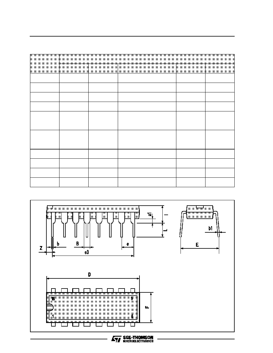
DIP16 PACKAGE MECHANICAL DATA
DIM.
mm
inch
MIN.
TYP.
MAX.
MIN.
TYP.
MAX.
a1
0.51
0.020
B
0.77
1.65
0.030
0.065
b
0.5
0.020
b1
0.25
0.010
D
20
0.787
E
8.5
0.335
e
2.54
0.100
e3
17.78
0.700
F
7.1
0.280
I
5.1
0.201
L
3.3
0.130
Z
1.27
0.050
L585
7/9

SO16 PACKAGE MECHANICAL DATA
DIM.
mm
inch
MIN.
TYP.
MAX.
MIN.
TYP.
MAX.
A
1.75
0.069
a1
0.1
0.2
0.004
0.008
a2
1.6
0.063
b
0.35
0.46
0.014
0.018
b1
0.19
0.25
0.007
0.010
C
0.5
0.020
c1
45
∞
(typ.)
D
9.8
10
0.386
0.394
E
5.8
6.2
0.228
0.244
e
1.27
0.050
e3
8.89
0.350
F
3.8
4.0
0.150
0.157
L
0.5
1.27
0.020
0.050
M
0.62
0.024
S
8
∞
(max.)
L585
8/9

Information furnished is believed to be accurate and reliable. However, SGS-THOMSON Microelectronics assumes no responsibility for
the consequences of use of such information nor for any infringement of patents or other rights of third parties which may result from its
use. No license is granted by implication or otherwise under any patent or patent rights of SGS-THOMSON Microelectronics. Specifica-
tions mentioned in this publication are subject to change without notice. This publication supersedes and replaces all information pre-
viously supplied. SGS-THOMSON Microelectronics products are not authorized for use as critical components in life support devices or
systems without express written approval of SGS-THOMSON Microelectronics.
©
1994 SGS-THOMSON Microelectronics - All Rights Reserved
SGS-THOMSON Microelectronics GROUP OF COMPANIES
Australia - Brazil - France - Germany - Hong Kong - Italy - Japan - Korea - Malaysia - Malta - Morocco - The Netherlands - Singapore -
Spain - Sweden - Switzerland - Taiwan - Thaliand - United Kingdom - U.S.A.
L585
9/9