 | –≠–ª–µ–∫—Ç—Ä–æ–Ω–Ω—ã–π –∫–æ–º–ø–æ–Ω–µ–Ω—Ç: L5951 | –°–∫–∞—á–∞—Ç—å:  PDF PDF  ZIP ZIP |

1/13
L5951
January 2001
s
3 VOLTAGE REGULATORS:
3.3V (100mA) STANDBY REGULATOR
5V (100mA) STANDBY REGULATOR
7.8V (100mA)
s
OUT OF REGULATION DETECTION FOR 5V-
STANDBY REGULATOR
s
WIDE OPERATING SUPPLY VOLTAGE
RANGE FROM 4.5V UP TO 26.5V FOR
TRANSIENT 34V
s
VERY LOW STANDBY QUIESCENT
CURRENT (<150
µ
A)
s
INPUT TO OUTPUT SIGNAL TRANSFER
FUNCTION PROGRAMMABLE
s
LVS FUNCTION
s
TTL AND CMOS COMPATIBLE INPUTS
s
OUTPUT CURRENT LIMITATION
s
CONTROLLED OUTPUT SLOPE FOR LOW
EMI
s
OVERTEMPERATURE SHUT-DOWN
s
ABLE TO SURVIVE UNDER LOSS OF
GROUND OR BATTERY
s
ESD PROTECTED
DESCRIPTION
The L5951 is a monolithic triple regulator integrated
with a SAE J1850 Integrated Driver / Receiver real-
ized in advanced Multipower-BCD technology. It is
intended to drive single wire J1850 communications,
and offer microcontroller power and power manage-
ment for automotive or industrial applications.
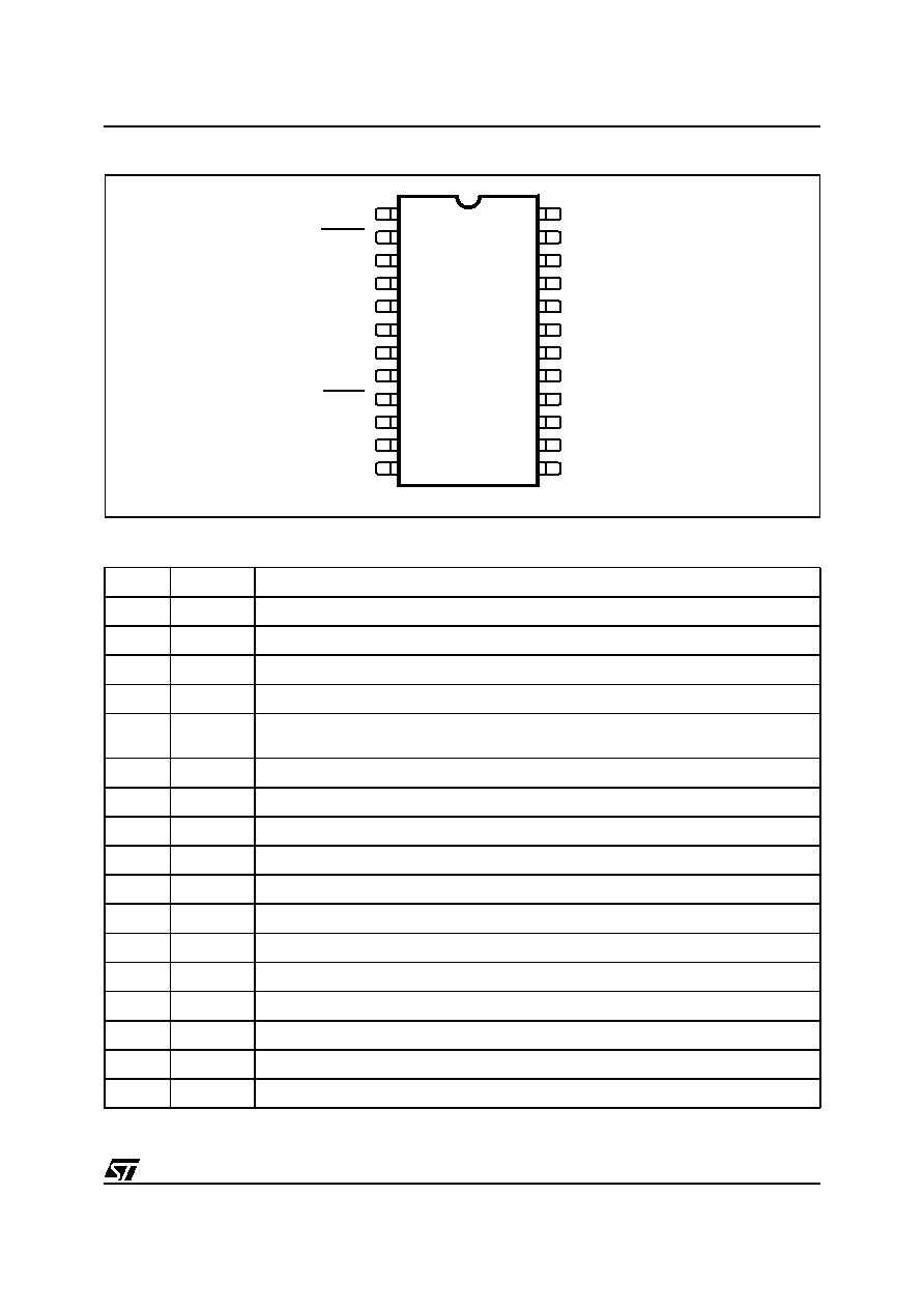
SO24
ORDERING NUMBER: L5951
TRIPLE OUTPUT MULTIFUNCTION VOLTAGE REGULATOR
FOR CAR RADIO WITH IDR/CLASS 2 INTERFACE
BLOCK DIAGRAM
SUPPLY
SELECTOR
BANDGAP
REFERENCE
3V
STANDBY
5V
STANDBY
RESET
ENABLE/
PROTECTION
LOGIC
7.8V
BUS DRIVER
WAVESHAPING
FILTER
4XEN AND
LOOPBACK
DIGITAL OUTPUT
DRIVER
LOSS
OF GND
PROTECTION
LOAD
GND
BUS
REG3
RESET
REG2
REG1
VBAT
LVS
EN
SLEEP
TX
4X
LOOP
RX
D99AU991

L5951
2/13
1
FUNCTIONAL DESCRIPTION
1.1 General Features
The L5951 is an integrated circuit which provides a J1850 physical layer as well three voltage regulators. The
L5951 was developed to provide the power and Class 2/IDR interface for a microcontroller.
1.2 REG1 Output Voltage
The REG1 regulator output is equal to 3.3V. The 3.3V regulator is non low drop out and can handle currents up
to 100mA with short citcuit limit of 280mA.
1.3 REG2 Output Voltage
The REG2 regulator output is equal to 5V and can handle currents up to 100mA with short citcuit limit of 280mA.
The output stage of the 5V regulator is low dropout.
1.4 REG3 Output Voltage
The REG3 regulator output is equal to 7.8V and can handle currents up to 100mA with short citcuit limit of
280mA. The output stage of the 7.8V regulator is low dropout. REG3 regulator is controlled by the EN (enable)
pin of the IC. REG3 can be turned on and off by toggling the EN pin. A logic "1" on the EN pin enables REG3,
while a logic "0" on the EN pin disables REG3. The maximum voltage when REG3 is off must be less than 0.2V.
Sleep* Input - The Class 2 transmitter can be turned on and turned off by the Sleep* pin. Once the voltage level
is above 2VDC, the transmitter is enabled. If the Sleep* pin drops below 0.8VDC, and EN is "0" the transceiver
goes into a low power mode. In low power mode, REG3 and the transceiver are disabled. The L5951 will still
receive messages and send them to the microcontroller out of the RX pin.
* denotes active low
LVS input - Reg1 and Reg2 are supplied by Vbat pin. The device could then dissipate a lot of power, causing
thermal shutdown at high voltage. For this reason a secondary low voltage supply (LVS) can be used to reduce
power dissipation.
Reset* Output - The L5951 has low voltage or no voltage circuitry that is a warning to the microcontroller. If
REG2 drops 0.3VDC below its normal operating voltage, the Reset* pin will go to a logic "0". Between the volt-
age levels of 4.65VDC (min) and 5.10VDC (max) on REG2, a reset will occur. There is a hysterisis of 50mV on
the Reset* pin.
* denotes active low
Low Input Voltage Operation - If battery voltage level drops below 7.0V, the outputs are to remain alive and
ready for the return of normal voltage battery levels. The L5951 will be able to retrieve data off the BUS and
send it to the micrprocessor when the supply voltage is as low as 4.9V. The regulators should stay the same
voltage as the battery voltage down to 7.0V minus operating headroom for the 7.8V regulator. BUS V
OH,min
are
not guaranteed over all conditions below VBAT = 9.0V.
Waveshaping - Messages sent by the microcontroller to the transceiver are routed to a waveshaping circuit.
The digital signal is rounded at the switching points in order to reduce EMI emissions. A second order function,
I = C*dV/dt, is used to control the rise and fall times of the transmission. The rise and fall times are controlled
by an external resistor Rext . The waveshaping circuit can be enabled and disabled by the 4X pin. A logic "1"
will disable the waveshape circuit and a logic "0" will enable the waveshape circuit. In 4X mode, the speed of
the BUS is increased by a factor of four. Any signal coming from the microcontroller and going to the BUS must
be waveshaped. If loopback(LOOP) is enabled, the signal coming from the micro through the TX pin is routed
to the RX pin back to the micro with or without it being waveshaped. A logic "1" enables loopback and a logic"0"
disables loopback.
Nodes - The transmitter provides a wave-shaped 0 to 7.7 VDC waveform on the BUS output. It also receives
waveforms and transmits a digital level signal back to a logic IC. The transmitter can drive up to 32 remote trans-
ceivers. These remote nodes may be at ground potentials that are ±2 VDC, with respect to the assembly. Under
this condition, waveshaping will only be maintained during 3 of the 4 corners. The L5951 is a remote node on
the Class 2/IDR Bus. Each remote transceiver has a 470 + 10% pF capacitor on its output for EMI suppression,

3/13
L5951
as well as a 10.6 kW + 5% pull down resistor to ground. The main node has a 3,300 + 10% pF capacitor on its
output for EMI suppression, as well as a 1.5 k
+ 5% pull down resistor to ground. With more than 26 nodes
there is no primary node , all nodes will have the 470 ±10% pF capacitor and the 10.6k
±
5% pull down resistor.
No matter how many remote nodes are on the Class 2/IDR Bus, the RC of the Class 2/IDR Bus is maintained
at approximately 5ms. The minimum and maximum load on the Class 2/IDR Bus is given below :
1.5 Protection
The L5951 can survive under the following conditions: shorting the outputs to BAT and GND, loss of BAT, loss
of IC GND, double battery(+26.5V), 4000V ESD, 34V load dump. L5951 will not handle a reverse battery con-
dition. External components must be implemented for reverse battery protection.
Thermal Shutdown: thermal shutdown is broken down into two areas; V1 and V2 ouputs, and the other is V3
output and the Class 2 Bus Driver. V1 and V2 outputs shutdown at 160∞C and returns to normal operation at
130∞C. The V3 output and Class 2 Bus Driver shutdown at 150∞C and return to normal operation at 120∞C.
Current Limiting: each voltage regulator will contain its own current protection, and the maximum allowable cur-
rent for all three regulators is 280mA.
Short Circuit: If the outputs are short circuited, the IC will begin current limiting and eventually the thermal shut-
down will kick in. Current limiting will not disable the outputs.
Overvoltage: The IC will not operate if the BAT voltage reaches 30V or above. V1 and V2 will not be shutdown,
but all other outputs will not operate.
Loss of Ground & Loss of Battery Connection: in this conditions a very small leakage on BUS is generated.
1.6 Protocol Description
The L5951 uses a Variable Pulse Width (VPW) modulated protocol. One frame consists of an entire message
not containing more than 12 bytes. The first bit of each byte will be the most significant bit (MSB). A transmitted
message begins with a SOF signal and ends with the EOF signal.
The data to be transmitted has to be in a specific format as follows:
idle,SOF,DATA, CRC, EOD, NB, IFR, EOF, IFS, idle
Definitions below:
idle:
Logic level low on communication bus
SOF:
Start of Frame
DATA: Data Bytes
CRC:
Cyclic Redundancy Check Error Detection Byte
EOD:
End of DATA(only when IFR is used)
NB: Normalization
Bit
IFR:
In-Frame Response Byte(s)
EOF:
End of Frame
IFS: Inter-Frame
Separation
BRK:
Break(can occur on network at any time)
Idle - Logic level low on bus any time after IFS.
Start of Frame (SOF) - The SOF signals the receiver that a new frame is beginning. SOF signal is a logic level
Capacitance
Resistance to Ground
Minimum Nodes
(3.33 ∑ .9) + (.47 ∑ .9) = 3.39 nF
(1.5 ∑ 1.05) || (10.6 ∑ 1.05) = 1.38 k
Maximum Nodes
(3.3 ∑ 1.1) + 25∑(0.47 ∑ 1.1) = 16.55 nF (1.5 ∑ 0.95) || (10.6 ∑ 0.95) / 25 = 314

L5951
4/13
high pulse identified by a pulse width of about t = 200
µ
s.
DATA - Total number of bytes that can be transmitted (from SOF to EOF) is 12 bytes.
Cyclic Redundancy Check (CRC) - A method for determining if the message received is the same as the mes-
sage transmitted. If an invalid CRC number is detected, then an error will be detected. The SOF signal is not
used to determine the CRC. All bits in the CRC are initially "ones" to avoid confusion with a data stream that are
all "zeros".
End of Data (EOD) - Used to signal the receiver about the end of data transmission. If there is a IRF signal, the
sender of the frame will expect one or more bytes in the IFR following the EOD. If there is no IFR used, then the
bus would stay in a logic level low state resulting in a EOF. EOD signal is recognized by a logic level low pulse
for a duration of about 200
µ
s.
Normalization Bit (NB) - The sole reason for the NB is to define the start of the in-frame response. The first bit
the the IFR is passive, therefore it is necessary to have a signal that follows EOD. There are two forms to the
NB. First of all, the NB is a logic level high pulse. The two forms are distinguished by thier pulse widths. The first
form has a pulse width of about 64
µ
s and indicates if the IFR contains a CRC or not. The second form has a
longer pulse width of about 128
µ
s and also indicates if there is a CRC in the IFR or not. The manufacturer can
manipulate the NB to any of the two methods.
In-Frame Response (IFR) - Response bytes are sent by the receiver of the transmission and start after the
EOD. If the IFR stays at a logic level low for a period of time then the frame must be considered to be complete.
IFR bytes can be used to send a signal back to the originator indicating the correct CRC number to confirm the
correct message was sent.
End of Frame (EOF) - Indicates the end of a frame. Once the last byte is transmitted, the bus will be in a logic
level low state for a period of time indicating the end of the frame. EOF signal is recognized by a low pulse for
a width of about 280
µ
s.
Inter-Frame Separation (IFS) - IFS is used to synchronize the receivers at various nodes.
ABSOLUTE MAXIMUM RATINGS
* denotes active low
THERMAL DATA
(*) With 6cm2 on board heat sink area.
Symbol
Parameter
Value
Unit
V
S
DC Operating Supply Voltage
-0.6 to 26.5
V
V
DIAG
Diagnostic output voltage
-0.6 to 5.5
V
V
IN
Input Control Voltage (EN, Sleep, 4X, Loop, TX)
-0.6 to 5.5
V
V
OUT
Output Control Voltage (Reset *)
-0.3 to 5.5
V
V
S
Peak Supply Voltage t = 50ms
34
V
T
op
Operating Temperature Range
-40 to 85
∞C
T
stg
Storage Temperature Range
-40 to 150
∞C
Symbol
Parameter
Value
Unit
R
th j-amb
Thermal resistance junction to ambient (*)
50
∞C/W
5/13
L5951
PIN CONNECTION
PIN FUNCTIONS
*denotes active low for Sleep and Reset.
N.
Name
Function
1
REG1
Regulator #1
2
Reset *
Reset Output to
µ
C
3
Rext
Waveshaping Resistor
4
GND_REG
Regulator Ground
,6,7,8,17,
18,19,20
GND_TX
Transceiver Ground
9
Sleep *
Transceiver Enable Input
0
EN
Enable for Regulator #3
11
4X
4XBus mode (41.6K Baud)
12
LOOP
Loopback Enable
13
RX
Serial Data Output to mC
14
TX
Serial Data Input from mC
15
Load
External Pull Down to Gnd
16
Bus
Bus Output to Vehicle
21
Bat
Battery Supply
22
REG3
Regulator #3
23
REG2
Regulator #2
24
LVS
Low Voltage Supply
REG1
RESET
REXT
GND_REG
GND_TX
GND_TX
GND_TX
GND_TX
SLEEP
BUS
GND_TX
GND_TX
GND_TX
GND_TX
BAT
REG3
REG2
LVS
1
3
2
4
5
6
7
8
9
22
21
20
19
18
16
17
15
23
10
24
EN
LOAD
D99AU992
4X
TX
11
14
13
12
LOOP
RX

L5951
6/13
ELECTRICAL CHARACTERISTICS
(T
amb
= 25∞C, V
BAT
= 14.4V unless otherwise specified. Standard Loads: I
REG1
= 0.5mA, I
REG2
= 0.5mA, I
REG3
= 5mA)
Symbol
Parameter
Test Condition
Min.
Typ.
Max.
Unit
I
q,ST-BY
Standby Quiescent Current
EN, Sleep* = 0V, V
BAT
= 14V,
I
REG2
= 50mA, I
REG1
= 50mA
EN, Sleep* = 0V, V
BAT
= 14V,
I
REG2
= 500
µ
A, I
REG1
= 250mA
350
110
µ
A
µ
A
Maximum QuiescentCurrent -
V
BAT
V
BAT
= 14V, I
REG1
= 100mA,
I
REG2
= 100mA, I
REG3
= 100mA,
I
BUS
= 30mA
LVS = 0V
LVS = 10V
10
10.5
mA
mA
Maximum QuiescentCurrent -
LVS
V
BAT
= 14V, I
REG1
= 100mA,
I
REG2
= 100mA, I
REG3
= 100mA,
I
BUS
= 30mA LVS = 10V
750
µ
A
EN Switch Input Current
V
BAT
= 14V, EN
2V
V
BAT
= 14V, EN
0.8V
0
0
µ
A
µ
A
V
ENL, ENH
EN Input Threshold Voltage
V
BAT
= 14V, VIL
V
BAT
= 14V, VIH
2
0.8
V
V
RES, L
Reset* Output Low Voltage
Set V
BAT
so V
REG2
drops 0.30V
0
0.02
0.4
V
V
RES
Reset* Output Voltage Threshold
Decrease V
BAT
so V
REG2
drops
until Reset* drops
V
REG2
- 0.20
V
V
RES, HYS
Reset Threshold Hysteresis
50
mV
(*) Denotes active low.
3.3V/100mA DC Characteristics for Regulator Output 1
V
REG1
Output Voltage
I
REG1
=100mA
3.14
3.3
3.46
V
V
line
Line Regulation
7V
V
BAT
26V
(Measure
V
REG1
Across V
BAT
Range)
7
15
mV
V
load
Load Regulation
0.5mA
I
REG1
100mA
(Measure
V
REG1
Across V
LOAD
Range)
8
50
mV
V
DROPOUT
Dropout Voltage (Measure V
BAT
-
V
REG1
when V
REG1
drops 0.1V)
I
REG1
= 100mA
I
REG1
= 5mA
1
0.12
2.2
1.5
V
V
I
lim1
Current Limit
200
mA
SVR1
Reg1 Supply Voltage Rejection
I
REG1
= I
REG2
= I
REG3
= 50mA
f = 20 to 20kHz
VBAT = 14Vdc, 1Vac,pp
45
dB
5V/100mA Regulator Output 2
V
REG2
Output Voltage
I
REG2
=100mA
4.75
5
5.25
V
V
line
Line Regulation
7V
V
BAT
26V
(Measure
V
REG2
Across V
BAT
Range)
6
40
mV
7/13
L5951
V
load
Load Regulation
0.5mA
I
REG2
100mA
(Measure
V
REG2
Across V
LOAD
Range)
14
100
mV
V
DROPOUT
Dropout Voltage (Measure V
BAT
-
V
REG2
when V
REG2
drops 0.1V)
I
REG2
=100mA
I
REG2
=5mA
450
22
mV
mV
I
lim2
Current Limit
200
mA
SVR2
Reg2 Supply Voltage Rejection
I
REG1
= I
REG2
= I
REG3
= 50mA
f = 20 to 20kHz
VBAT = 14Vdc, 1Vac,pp
45
dB
7.8V/100mA Regulator Output 3
V
REG3
Output Voltage
I
REG3
=100mA - 8.8V
V
BAT
Range
7.60
7.8
8
V
DV
line
Line Regulation
8.8V
V
BAT
26V
(Measure
V
REG3
Across V
BAT
Range)
50
mV
DV
load
Load Regulation
5mA
I
REG3
100mA
(Measure
V
REG3
Across V
LOAD
Range)
50
mV
V
DROPOUT
Dropout Voltage
(Measure V
BAT
- V
REG3
when
V
REG3
drops 0.1V)
I
REG3
= 100mA
I
REG3
= 5mA
0.5
0.04
V
V
I
lim3
Current Limit
200
mA
SVR3
Reg3 Supply Voltage Rejection
I
REG1
= I
REG2
= I
REG3
= 50mA
f = 20 to 20kHz
VBAT = 14Vdc, 1Vac,pp
45
dB
DC Characteristics for Class 2 Transceiver
Standard Loads: I
REG1
= 0.5mA, I
REG2
= 0.5mA, I
REG3
= 5mA
BUS
ih
BUS
il
BUS Guaranteed
Input Voltages
Verify RX > 3 VDC
Verify RX < 3 VDC
4.25
3.7
3.50
V
V
BUS
Hyst
BUS Hysteresis
BUS
Itoh
- BUS
hhtol
0.15
V
BUSov
BUS Output Voltage
TX = 5 VDC,
BUS = 257 to 1380
to gnd
V
BAT
- 8.2 to 16 VDC
V
BAT
- 6.0 to 8.2 VDC
TX = 0V
7.2
5
V
V
I
BUSshort
BUS Short Circuit Current
TX = 5VDC
BUS = -2 to 4.8VDC
170
mA
I
BUSleak
BUS Leakage Current
BUS = -2 to 0 VDC
BUS = 0 to V
BAT
0
0
mA
mA
LOAD
ON
Load Output
I
LOAD
= 6mA
0.045
V
ELECTRICAL CHARACTERISTICS (continued)
(T
amb
= 25∞C, V
BAT
= 14.4V unless otherwise specified. Standard Loads: I
REG1
= 0.5mA, I
REG2
= 0.5mA, I
REG3
= 5mA)
Symbol
Parameter
Test Condition
Min.
Typ.
Max.
Unit
L5951
8/13
LOAD
Dio
Load Output (Unpowered)
V
BAT
= 0V, I
LOAD
= 6mA
0.7
V
I
BUSloss
I
LOADloss
BUS & LOADCurrent during loss
of assembly V
BAT
or GND
I
VBAT
= 0mA,
BUS = -18 to 9VDC
LOAD = -18 to 0 VDC
11
39
µ
A
µ
A
TX
VIL
TX
VIH
TX Input Voltage
Verify BUS < 3.875VDC
Verify BUS > 3.875VDC
2
0.8
V
V
I
TXVIL
I
TXVIH
TX Input Current
TX = 5VDC
TX = 0VDC
110
0
µ
A
µ
A
4
Trip1
4
Trip2
4X Input Trip Point Voltages
Normal Mode
4X Mode
1.4
V
I
4Xvih
I
4Xvil
4X Input Current
4X = 5 VDC
4X = 0 VDC
0
0
µ
A
µ
A
L
Trip1
L
Trip2
LOOP Input Trip Point Voltages
Normal Mode
Loopback Mode
2
0.8
V
V
I
Lvih
I
Lvil
LOOP Input Current
LOOP = 5VDC
LOOP = 0VDC
0
µ
A
V
RXhigh
RX Output Voltage, High
BUS = 7V, I
RX
= -200
µ
A
4.85
V
V
RXlow
RX Output Voltage, Low
BUS = 0V, I
RX
= 1.6mA
0.2
V
I
RX
RX Output Current
RX = high (Short circuit protection
limits)
5
mA
Sleep* V
IH
Sleep*V
IL
Sleep* Input Voltage
TX = 5VDC
Verify BUS > 3.725
Verify BUS < 4.025
2
0.8
V
V
I
Sleepvih
I
Sleepvil
Sleep* Input Current
Sleep* = 5VDC
Sleep* = 0VDC
0.2
0
µ
A
µ
A
* Denotes active low for Sleep and Reset.
AC Characteristics for Class 2 Transceiver
Standard Loads: IREG1 = 0.5mA, IREG2 = 0.5mA, IREG3 = 5mA
BUS
LTOH
BUS Voltage Rise Times
TX = 7.812Hz square wave
See Figure 1
Min and Max Loaded BUS
15
µ
s
BUS
HTOL
BUS Voltage Fall Times
TX = 7.812Hz square wave
See Figure 1
Min and Max Loaded BUS
14
µ
s
t
Wbus
BUS Pulse Width Distortion
TX = 7.812Hz square wave
See Figure 2
Load BUS with 3.300pF and
1.38k
Meas. @ 1.5V levels
Meas. @ 6.25V levels
77
48
µ
s
µ
s
ELECTRICAL CHARACTERISTICS (continued)
(T
amb
= 25∞C, V
BAT
= 14.4V unless otherwise specified. Standard Loads: I
REG1
= 0.5mA, I
REG2
= 0.5mA, I
REG3
= 5mA)
Symbol
Parameter
Test Condition
Min.
Typ.
Max.
Unit

9/13
L5951
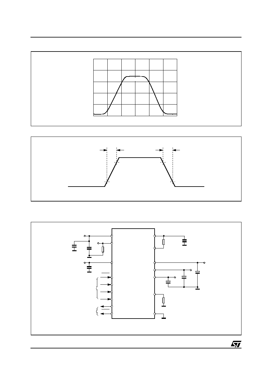
2
BUS TIMING DIAGRAM
Figure 1. BUS Rise and Fall Times
Figure 2. BUS Pulse Width Distortion
V1
V2
Spectral Content Limit
(Measure spectral peak from
0.53MHz to 1.6MHz)
V
BAT
= 9V to 16V, no ground
offset, 0.53
f
1MHz.
V
BAT
= 9V to 16V, no ground
offset, 1
f
1.67MHz.
100
80
µ
V
µ
V
BUS
DLY
Propagation Delay
Measure Delay Between TX Trip
Point and RX Trip Point
16
µ
s
TX
4XDLY
TX
NormDLY
TX to BUS Delay
Measure from 2.5V on TX to
3.875V on BUS
4X Mode
Normal Mode
3.5
14.5
µ
s
µ
s
RX
LTOHdly
RX
HTOLdly
RX Output Delay Time
See Figure 4
Measured from BUS Threshold
Voltage
1.5
1.9
µ
s
µ
s
RX
LTOH
RX
HTOL
RX Output Transition Time
Load RX with 50pF to Ground
See Figure 5
170
70
ns
ns
RX
LTOH
RX
HTOL
RX Output Transition Time During
Sleep State
Load RX with 50pF to Ground
See Figure 5, Sleep* = 0VDC
170
70
ns
ns
ELECTRICAL CHARACTERISTICS (continued)
(T
amb
= 25∞C, V
BAT
= 14.4V unless otherwise specified. Standard Loads: I
REG1
= 0.5mA, I
REG2
= 0.5mA, I
REG3
= 5mA)
Symbol
Parameter
Test Condition
Min.
Typ.
Max.
Unit
64
µ
sec
TX
5V
0V
6.25V
BUS
1.5V
trise
tfall
6.25V
1.5V
D99AU993
64
µ
sec
TX
5V
0V
6.25V
BUS
1.5V
D99AU994
3.875V
>35
µ
sec
64
µ
sec
<93
µ
sec
L5951
10/13
Figure 3. BUS Output Voltage
Figure 4. BUS to RX Delay Times
3
TYPICAL APPLICATION CURCUIT
Figure 5. Application Circui
D99AU995
20
40
60
80
100
0
4
5
6
7
8
V
time(
µ
s)
BUS
10%
RX
t
ltoh
t
htol
D99AU997
90%
90%
10%
VBATT
EN
10V
C1
0.1
µ
F
R1
47K
C8
0.1
µ
F
BAT
EN
LVS
SLEEP
4X
LOOP
TX
RX
RESET
FROM
LOGIC
TO
LOGIC
BUS/BUS OUT
LOAD/BUS IN
R2
10.7K
C7
10
µ
F
C5
10
µ
F
C3
10
µ
F
7.8VSW
5VSB
3.3VSB
REG1
REG2
REG3
REXT
R3
68K
GND
D99AU998mod
C9
470pF
C10
470
µ
F
Note: ESR of output capacitors should be between 0.2
and 5.0
.
11/13
L5951
4
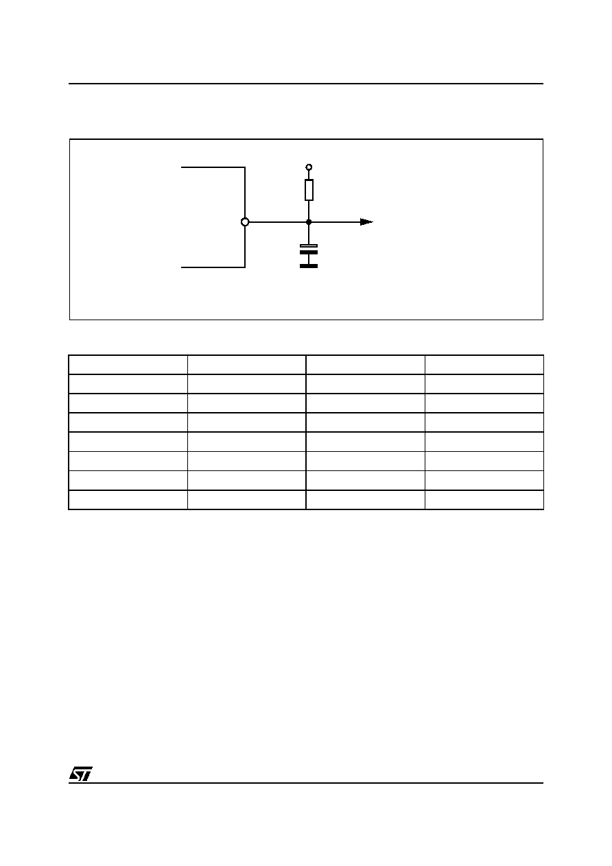
TYPICAL RESET CIRCUIT
Figure 6. Reset Circuit
External Components Parts List for Standard Application
Notes: (Reasons for This Component Choice)
1. Noise Suppression
2. Output Compensation
3. Pull Down Resistor
4. Bus Resistor
5. Bus Slew Rate Control
6. Proper Bus Capacitance
Quantity
Application Description
Part Description
Note Number
5
C1, C8
CAP - 0.1
µ
F, 25V
1
3
C3, C5, C7
CAP - Tant 10
µ
F, 10V
2
1
R1
RES-47k, 1/16W 5%
3
1
R2
RES - 10.7k, 1/16W, 1%
4
1
R3
RES - 68k, 1/16W, 1%
5
1
C9
CAP - 25V, 470pF
6
1
C10
CAP - 50V, 470pF
1
RESET
R
C
5VSB
to micro
D99AU999
1) 10k
is the minimum resistance for R.
2) The value of C depends on timing needed

L5951
12/13
SO24
DIM.
mm
inch
MIN.
TYP.
MAX.
MIN.
TYP.
MAX.
A
2.35
2.65
0.093
0.104
A1
0.10
0.30
0.004
0.012
A2
2.55
0.100
B
0.33
0.51
0.013
0.0200
C
0.23
0.32
0.009
0.013
D
15.20
15.60
0.598
0.614
E
7.40
7.60
0.291
0.299
e
1.27
0,050
H
10.0
10.65
0.394
0.419
h
0.25
0.75
0.010
0.030
k
0
∞
(min.), 8
∞
(max.)
L
0.40
1.27
0.016
0.050
B
e
A2
A
1
13
24
D
L
H
A1
C
E
K
h x 45∞
SO24
Seating Plane
0.10mm
.004
A1
OUTLINE AND
MECHANICAL DATA
12

Information furnished is believed to be accurate and reliable. However, STMicroelectronics assumes no responsibility for the consequences
of use of such information nor for any infringement of patents or other rights of third parties which may result from its use. No license is granted
by implication or otherwise under any patent or patent rights of STMicroelectronics. Specifications mentioned in this publication are subject
to change without notice. This publication supersedes and replaces all information previously supplied. STMicroelectronics products are not
authorized for use as critical components in life support devices or systems without express written approval of STMicroelectronics.
The ST logo is a registered trademark of STMicroelectronics
Æ
2001 STMicroelectronics - All Rights Reserved
STMicroelectronics GROUP OF COMPANIES
Australia - Brazil - China - Finland - France - Germany - Hong Kong - India - Italy - Japan - Malaysia - Malta - Morocco - Singapore - Spain
- Sweden - Switzerland - United Kingdom - U.S.A.
http://www.st.com
13/13
L5951