 | –≠–ª–µ–∫—Ç—Ä–æ–Ω–Ω—ã–π –∫–æ–º–ø–æ–Ω–µ–Ω—Ç: L5953 | –°–∫–∞—á–∞—Ç—å:  PDF PDF  ZIP ZIP |

1/24
L5953
September 2003
This is preliminary information on a new product now in development. Details are subject to change without notice.
s
PWM: ADJUSTABLE 2.5/10V - 1A
SWITCHING VOLTAGE REGULATOR
s
EXTERNAL POWER MOS ABILITY FOR
OUTPUT CURRENT ENHANCEMENT
s
SYNCHRONIZATION FUNCTION
s
REG1- LINEAR LOW DROP 3.3/5V - 250mA
STBY VOLTAGE REGULATOR (LOW
CURRENT CONSUMPTION) with RESET
s
REG2- LINEAR VOLTAGE REGULATOR 1.5V
to 3.3V EXTERNALLY ADJUSTABLE - 300mA
MAXIMUM CURRENT
s
HSD1 : 500mA HIGH SIDE DRIVER
s
HSD2 : 200mA HIGH SIDE DRIVER
s
SPI INTERFACE
s
SPI DIAGNOSTICS HSD1, HSD2
s
DOUBLE SWITCHING FREQUENCY SPI
SELECTABLE
s
DOUBLE INPUT LVW
SPI FUNCTIONS
s
INPUT CONTROLS
≠ Turn-on/off PWM
≠ Turn-on/off REG2
≠ Turn-on/off HSD1
≠ Turn-on/off HSD2
≠ Switching frequency selection f1- f2
s
OUTPUT FUNCTIONS:
≠ HSD1 & HSD2 short to gnd, open load and
short to battery (Test mode)
≠ Thermal warning
PROTECTIONS
s
OVERVOLTAGE PROTECTION
s
INTERNAL CURRENT LIMITING
s
THERMAL SHUTDOWN
s
ESD
DESCRIPTION
The L5953 is the integration of one switching regula-
tor, two linear voltage regulators, two low voltage
warnings and two high side drivers. It has a stand-by
operation mode (low current consumption) where
only the stand-by voltage regulator plus the low volt-
age warnings are active. The other regulators and
high side drivers are controlled by the SPI interface.
PowerSO36
ORDERING NUMBER: L5953
PRODUCT PREVIEW
MULTIPLE SWITCHING VOLTAGE REGULATOR
BLOCK DIAGRAM
VOLTAGE WARNING
SPI INTERFACE
REC2
LINEAR VOLTAGE
REGULATOR
1.5-3.3V/300mA
HSD1
HSD1
HSD2
HSD2
COMP
FB
GATEOUT
GATEIN
VSW
DRAINOUT
STRAP
ADJ
VSTBY
GND
SWGND
S1
W1
S2
W2
VDD-LIN
REC1
ST-BY LINEAR VOLTAGE
REGULATOR
3.3-5V/250mA
PWM
STEP DOWN
REGULATOR
2.5-10V/1A
OSCILLATOR &
SYNC
STCAP
CT
RES
VDD-SW
IRQ
Q
D
S
C
VLR
FBLR
VIN
SYNC
VSPI
DGND
FGND
D01AU1330A

L5953
2/24
ABSOLUTE MAXIMUM RATINGS
THERMAL DATA
PIN CONNECTION
Symbol
Parameter
Value
Unit
V
DD
DC Operating Supply Voltage
-0.6 to 30
V
Transient Supply Overvoltage (250ms)
50
V
V
SPI
Supply Voltage for SPI I/O
-0.6 to 6
V
I
O
Voltage Regulator Output Current
Internally limited
V
inlog
Input Voltage (C,D,Q,
S
,SYNC)
0 to 6
V
RESR
Output Capacitor Series Eq. Resistance (Linear reg.)(Allowed
range)
From 0.2 to 10
T
op
Operating Temperature Range
-40 to 85
∞C
T
stg
Storage Temperature Ranges
-55 to 150
∞C
T
j
Operative Junction Temperature
-40 to 150
∞C
Symbol
Parameter
Value
Unit
R
thj-case
Thermal Resistance Junction to Case
1.7
∞C/W
FGND
S2
S1
W2
IRQ
VDD-LIN
HSD2
N.C.
HSD1
DRAINOUT
N.C.
GND
GATEIN
VSW
STCAP
VSPI
VSTBY
ADJ
18
16
17
15
6
5
4
3
2
21
22
31
32
33
35
34
36
20
1
19
SWGND
VDD-SW
D02AU1345A
Q
DGND
S
GATEOUT
SYNC
STRAP
9
8
7
28
29
30
C
VLR
10
27
W1
D
CT
VIN
FB
FBLR
14
12
11
23
25
26
RES
COMP
13
24

3/24
L5953
PIN FUNCTION
Pin Number
Pin Name
Function
1
FGND
Analog Ground
2
S2
Input Voltage for LVW2
3
S1
Input Voltage for LVW1
4
W2
LVW2 Output
5
W1
LVW1 Output
6
RES
Reset
7
CT
Timing capacitor
8
D
SPI Serial Input
9
C
SPI Clock
10
Q
SPI Serial Output
11
S
SPI Chip Select
12
DGND
SPI Ground
13
IRQ
Interrupt
14
HSD2
HSD2 Output
15
VDD-LIN
Battery
16
N.C.
Not Connected
17
HSD1
HSD1 Output
18
SWGND
Switching Ground
19
VDD-SW
PWM Battery
20
DRAINOUT
Drain of the exrternal MOS
21
N.C.
Not Connected
22
GND
Ground
23
VSW
Source of the external MOS
24
GATEIN
Gate of the internal MOS
25
GATEOUT
Switching Output for power mos gate
26
STRAP
Bootstrap
27
SYNC
Synchronization
28
VLR
REG2 Linear Voltage Regulator Output
29
VIN
REG2 Linear Voltage Regulator Input
30
FBLR
REG2 Linear Voltage Regulator Feedback
31
COMP
PWM Compensation
32
FB
PWM Feedback
33
STCAP
ST-CAP
34
VSPI
Supply Voltage for SPI I/O
35
VSTBY
REG1 Stand-by Linear Voltage Regulator Output
36
ADJ
3.3V/5V REG1 Voltage Select

L5953
4/24
ELECTRICAL CHARACTERISTCS
( T
amb
= 25∞C, V
DD
= 14.4V)
Symbol
Parameter
Test Condition
Min.
Typ.
Max.
Unit
I
Q,STBY
Quiescent current with regulators
and High-side drivers off
W1, W2, RES, IRQ, not active;
REG2, HSD1, HSD2, PWM off;
S, C, D fixed at high/low logic
level
100
µ
A
T
sd
Thermal Shutdown Junction
Temperature
150
∞C
SMPS.PWM
T
amb
= 25∞C, V
DD
= 14.4V, V
o
= 5V; unless otherwise specified.)
V
o,min
Minimum Output Voltage
I
o
= 200mA
2.4
2.5
2.6
V
V
o,max
Maximum Output Voltage
I
o
= 200mA
9.6
10
10.4
V
Vref,PWM
Voltage Reference
1.275
V
V
i
Input Voltage Range
V
o
= 5V; I
o
= 0.5A
6
18
V
V
o
Line Regulation
I
o
= 0.5A
100
mV
V
o
Load Regulation
V
o
= 5V; I
o
= 0.2A to 0.5A
50
mV
V
d
Dropout Voltage between Pin 19
and Pin 23
I
o
= 0.5A, V
o
= 5V
0.5
V
I
o
= 1A, V
o
= 5V
1
V
I
Lim
Current Limit
1.5
A
Efficiency
f = 260kHz; I
o
= 0.5A
f = 400kHz; I
o
= 0.5A
90
86
%
%
SVR
Supply Voltage Ripple Rejection
V
i
= 1Vrms;
f
ripple
= 300Hz; I
o
= 0.4A
50
dB
OSCILLATOR
f
1
Swiching frequency
249
260
271
kHz
f
2
Swiching frequency
384
400
416
kHz
Voltage Stability of Switching
Frequency
V
DD
= 8 to 18V
Tbd
%
Temperature Stability of Switching
Frequency
T
j
= -40∞C to 85∞C
Tbd
%
SYNC
V
IL
Low Input Voltage
0.8
V
V
IH
High Input Voltage
2
V
V
OL
Low Output Voltage
0.4
V
V
OH
High Output Voltage
I
SOURCE
=1.5mA
4
V
f
V
i
---------
f
T
j
---------

5/24
L5953
I
SLAVE
Slave Sink Current
100
µ
A
T
W
Output Pulse Width
300
ns
REG1 - 3.3V/5V STBY LINEAR VOLTAGE REGULATOR
V
STBY
Output Voltage
no load; ADJ pin = open
no load; ADJ pin = VSTBY pin
4.9
3.20
5
3.3
5.1
3.4
V
V
V
line
Line Regulation
no load; 7 < Vdd < 26V
5
50
mV
V
load
Load Regulation
5mA < I
o
< 250mA
12
80
mV
V
dropout
V
STCAP
- V
STBY
I
o
= 100mA, V
o
= 5V
I
o
= 100mA, V
o
= 3.3V
0.36
0.47
0.5
0.65
V
I
lim
Current Limit
Out short to GND
300
mA
SVR
Supply Voltage Rejection
V
DD
= 1Vrms: f = 300Hz
I
o
= 250mA
55
dB
REG2 - LINEAR VOLTAGE REGULATOR 1.5V to 3.3V
V
LR
Linear Regulator Output Voltage
no load; 4.75
V
IN
16V;
1+ (R5/R6) = 2.588
3.2
3.3
3.4
V
no load; 3.135
V
IN
16V;
1+ (R5/R6) = 1.176
1.45
1.5
1.55
V
IN
Input Voltage
I
O
= 150mA
1.5V
V
LR
2V
3.135
16
V
I
O
= 300mA
1.5V
V
LR
3.3V
4.75
16
V
V
load
Load Regulation
5mA
I
O
300mA
4.75V
V
IN
16V; 1.5V
V
LR
3.3V
12
mV
V
line
Line Regulation
no load;
4.75V
V
IN
16V; 1.5V
V
LR
3.3V
1
mV
V
ref,REG2
Voltage Reference
1.275
V
I
Lim
Current Limit
Out Short to ground
400
mA
SVR
Supply Voltage Rejection
V
IN
= 5Vdc, 0.5Vacpp, 300Hz
I
O
= 300mA; 1.5V
V
LR
3.3V
55
dB
V
IN
= 3.3Vdc, 0.5Vacpp, 300Hz
I
O
= 150mA; 1.5V
V
LR
2V
55
dB
HSD1
V
sat, peak
Saturation Voltage
I
O
= 0.5A
250
mV
I
lim
Current Limit
600
mA
L
load
Load Inductance
100
mH
ELECTRICAL CHARACTERISTCS (continued)
( T
amb
= 25∞C, V
DD
= 14.4V)
Symbol
Parameter
Test Condition
Min.
Typ.
Max.
Unit

L5953
6/24
DIAGNOSTIC PARAMETERS
HSD2
V
sat, peak
Saturation Voltage
I
O
= 0.2A
250
mV
I
lim
Current Limit
300
mA
L
load
Load Inductance
100
mH
VOLTAGE WARNING
V
st
Sense Low Threshold
1.245
1.275
1.305
V
V
sth
Sense Threshold Hysteresis
35
45
60
mV
V
SL
Sense Output Low Voltage
I
o
= 1mA
0.4
V
I
SH
Sense Output Leakage
V
W
= 5V; V
SI
1.5V
10
µ
A
I
SI
Sense Input Current
V
SI
=5V
1
µ
A
RESET
V
RT
Reset Threshold Voltage
0.95 x
V
STBY
V
V
RTH
Reset Threhold Hysteresis
0.02 x
V
STBY
V
V
RL
Reset Output Voltage
I
o
= 1mA
0.4
V
I
RH
Reset Output Leakage
V
RT
= V
STBY
10
µ
A
V
CTth
Delay Comparator Threshold
0.5 x
V
STBY
V
CThy
Delay Comparator Threshold
Hysteresys
180
mV
I
CT1
Timing Capacitor Output Source
Current
7.5
µ
A
R
CT2
Timing Capacitor Output Pull-
Down equivalent Resistor
150
Symbol
Parameter
Test Condition
Min.
Typ.
Max.
Unit
HSD1W1 High Side Driver 1 Overcurrent
Warning activation
0.95
A
HSD1W2 High Side Driver 1 Open Load
Warning activation
HSD1 output voltage in test mode
3
V
HSD1W2
TEST
High Side Driver 1 V
DD
Short
Warning activation in test mode
HSD1 in test mode
Measure V
VDD-LIN
-V
HSD1
1.5
V
HSD2W1 High Side Driver 2 Overcurrent
Warning activation
0.7
A
ELECTRICAL CHARACTERISTCS (continued)
( T
amb
= 25∞C, V
DD
= 14.4V)
Symbol
Parameter
Test Condition
Min.
Typ.
Max.
Unit

7/24
L5953
SPI INTERFACE
HSD2W2 High Side Driver 2 Open Load
Warning activation
HSD2 output voltage in test mode
3
V
HSD2W3 High Side Driver 2 V
DD
Short
Warning activation in test mode
HSD2 in test mode
Measure V
VDD-LIN
-V
HSD1
1.5
V
THW
Thermal warning activation
145
∞C
IRQ - Interrupt Request Pin
IRQ-L
IRQ Low voltage
I
o
= 1mA
0.4
V
IRQ-H
IRQ Leakage
V
irq
= 5V
1
µ
A
Symbol
Alt
Parameter
Test Conditions
Min.
Max.
Unit
Recommended DC Operating Voltage
V
SPI
Supply Voltage for SPI I/O
3
5.5
V
Input Parameters (Tamb = 25∞C, f = 1MHz)
C
IN
Input Capacitance (D)
8
pF
C
IN
Input Capacitance (others pins)
6
pF
t
LPF
Input Signal Pulse Width
10
ns
DC Characteristics (T
amb
= -40 to 85∞C, V
SPI
= 3V to 5.5V)
I
LI
Input Leakage Current
2
µ
A
I
LO
Output Leakage Current
±2
µ
A
V
IL
Input Low Voltage
-0.3
0.3V
SPI
V
V
IH
Input High Voltage
0.7V
SPI
V
SPI
+1
V
V
OL
Output Low Voltage
I
OL
= 2mA
0.2V
SPI
V
V
OH
Output High Voltage
I
OH
= -2mA
0.8V
SPI
V
AC Characteristics (Tamb = -40 to 85∞C, V
SPI
= 3V to 5.5V
t
SCLH
t
SU
S Setup Time
50
ns
t
CLSH
t
SH
S Hold Time
50
ns
t
CH
t
WH
Clock High Time
200
ns
t
CL
t
WL
Clock Low Time
300
ns
t
CLCH
t
RC
Clock Rise Time
1
µ
s
t
CHCL
t
FC
Clock Fall Time
1
µ
s
t
DVCH
t
DSU
Data In Setup Time
50
ns
t
CHDX
t
DH
Data In Hold Time
50
ns
t
DLDH
t
RI
Data In Rise Time
1
µ
s
Symbol
Parameter
Test Condition
Min.
Typ.
Max.
Unit
L5953
8/24
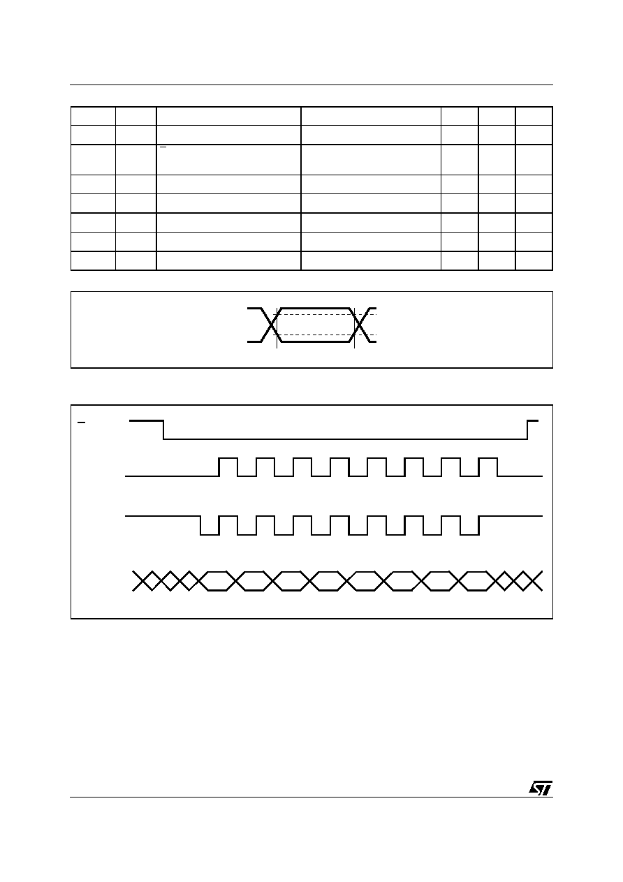
Figure 1. AC Testing Input Output WaveformsI
Figure 2. SPI Clocking Scheme
t
DHDL
t
FI
Data in Fall Time
1
µ
s
t
SHSL
t
CS
S Deselect Time
4.5V < V
SPI
< 5.5V
3V < V
SPI
< 4.5V
200
250
ns
ns
t
SHQZ
t
DIS
Output Disable Time
150
ns
t
QVCL
t
V
Clock Low to Output Valid
250
ns
t
CLQX
t
HO
Output Hold Time
0
ns
t
QLQH
t
RO
Output Rise Time
100
ns
t
QHQL
t
FO
Output Fall Time
100
ns
Symbol
Alt
Parameter
Test Conditions
Min.
Max.
Unit
0.8V
SPY
0.2V
SPY
0.7V
SPY
0.3V
SPY
D03AU1479
C
S
(MODE 0: CPOL=0,CPHA=0)
(MODE 3: CPOL=1,CPHA=1)
C
MSB
6
5
4
3
2
1
0
D
Q

9/24
L5953
Figure 3. Output Timing
Figure 4. Serial Input Timing
FUNCTIONAL DESCRIPTION
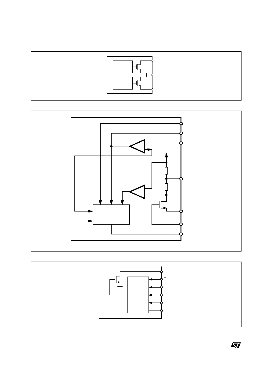
REG1 Stand-by Regulator (Figure 5)
The stand-by regulator output voltage can be 5V or 3.3V. It is externally selectable by means of the ADJ pin:
- leaving the ADJ pin open, the output voltage is 5V;
- connecting the ADJ pin to the Vstby pin the output voltage becomes 3.3V.
This regulator is supplied by STCAP pin and provide the reset information.
It has a current protection which limits the maximum allowable output current.
Reset (Figure 6)
The RES pin is an open collector that is activated (that is forced to zero) when the stand-by regulator is not in
regulation (including thermal shutdown and faults). The indication that REG1 is in regulation is delayed by a time
C
Q
AI01070B
S
MSB OUT
MSB-1 OUT
LSB OUT
D
ADDR.LSB IN
tSHQZ
tCH
tCL
tQLQH
(CPOL=0, CPHA=0)
tQHQL
tCLQX
tQVCL
C
D
AI01071
S
MSB IN
Q
tDVCH
HIGH IMPEDANCE
LSB IN
tSLCH
tCHDX
tDLDH
tDHDL
tCHCL
tCLCH
tCLSH
tSHSL
(CPOL=0, CPHA=0)

L5953
10/24
set up by the external capacitor CT.
When the RES is switched on, HSD1, HSD2, REG2, PWM are turned off and until the RES is forced to zero
only the REG1 and low Voltage Warnings are active.
Low Voltage Warning(Figure 7)
This circuit is able to sense two different voltages through external resistors to increase the overall flexibility.
If S1 pin voltage is higher than Vst, the output mos M1 is off: W1 is floating and can be pulled up by an external
resistor. If S1 pin voltage goes down and becomes lower than Vst, the mos M1 is turned on and forces W1 to
zero. The same thing happens for S2 - W2.
The outputs W1 and W2 can be connected together to get a single output.
REG2 Linear Voltage Regulator (Figure 5)
REG2 is a linear voltage regulator with a dedicated supply pin VIN. The output voltage (between 1.5V and 3.3V)
is fixed by an external divider. It can be turned on/off by SPI. It has a current protection which limits the maximum
allowable output current.
High Side Drivers (Figure 8)
Two high-side driver with charge pump controlled by SPI are available inside L5953. They are protected against
short to ground: the short circuit potection limits the maximum output current.
A diagnostic procedure is available to detect open load, short to battery and overcurrent.
Open load and short to battery can be reveal only in test mode while overcurrent is active only during normal
operationof the device. (see OPERATION -page 13
PWM Step Down Voltage Regulator (Figure 9)
The switching regulator inside the L5953 is a voltage control mode (also known as "direct duty cycle") Buck reg-
ulator: the error signal coming from the error amplifier is compared with a sawtooth to set on and off times of the
power switch.
The feedforward control is introduced to get a quickly response to input voltage changes: the sawtooh has a
fixed frequency and an amplitude variable with the battery voltage.
Continuous mode operation is recommended in order to reduce the stress of the output capacitor and of the
free-wheeling diode.
Error amplifier and compensation network
The error amplifier (EA) is a voltage amplifier whose non-inverting input is fixed to the reference voltage (1.275V
bandgap voltage) and whose inverting input and output are externally available for feedback and frequency
compensation.

11/24
L5953
Figure 5. Linear regulators - Internal pin connections
Figure 6. Reset Internal pin Connection
Figure 7. Low Voltage Warning Block Diagram.
POWER MOS
V
STBY
V
STBY
CONTROLLER
LINEAR REGULATOR
CONTROLLER
V
REF
1.275V
V
REF
1.275V
STCAP
VSTBY
ADJ
FGND
FBLR
VLR
VIN
POWER MOS
D03AU1493
Vref
2.5V/1.65V
FROM VST-BY
RES
CT
Vref 1.275V
7.5
µ
A
D03AU1480
S2
S1
V1
V2
W2
W1
M2
Vref =1.275V
+
-
M1
D03AU1478
Vref =1.275V
+
-
L5953
12/24
Figure 8. HSD - Internal pin connections
Figure 9. PWM - Internal pin connections
Figure 10. SPI & IRQ Internal pin connections
HSD2
VDD-LIN
HSD1
HSD2
CONTROLLER
HSD1
CONTROLLER
POWER
MOS
HSD1
POWER
MOS
HSD2
D01AU1333
PWM
CONTROLLER
VREF
1.275V
FROM THE
OSCILLATOR
ERROR AMPLIFIER
CURRENT
SENSING
DRAINOUT
R
S2
R
S1
POWER
MOS
VDD-SW
FB
COMP
STRAP
VSW
GATEOUT
GATEIN
D03AU1482
SPI
INTERFACE
IRQ
Q
S
D
DGND
C
D03AU1481

13/24
L5953
SPI INTERFACE
Signals Description (Figure 10)
The SPI interface available inside L5953 is able to work both in Mode 0 and Mode 3.
Serial Output (Q). The output pin is used to transfer data serially out of the L5953. Data is shifted out on the
falling edge of the serial clock.
Serial Input (D). The input pin is used to transfer data serially into the device. It receives instructions, address-
es, and data to be written. Input is latched on the rising edge of the serial clock.
Serial Clock (C). The serial clock provides the timing of the serial interface. Instructions, addresses, or data
present at the input pin are latched on the rising edge of the clock input, while data on the Q pin changes after
the falling edge of the clock input.
Chip Select (S). This input is used to select the L5953. The chip is selected by a high to low transition on the
S pin. At any time, the chip is deselected by a low to high transition on the S pin. As soon as the chip is dese-
lected, the Q pin is at high impedance state. The pin allows multiple L5953 to share the same SPI bus. After
power up, the chip is at the deselect state.
SPI Input/Output are supplied by an external supply voltage VSPI while the core is supplied by the stand-by
regulator VSTBY. The SPI is resetted by an internal signal whose buffered version is RES .
OPERATIONS
All instructions, addresses and data are shifted in and out of the chip MSB first. Data input (D) is sampled on
the first rising edge of clock (C) after the chip select (S) goes low. Prior to any operation, a one-byte instruction
code must be entered in the chip. This code is entered in the chip. This code is entered via the data input (D),
and latched on the rising edge of the clock input (C). To enter an instruction code, the product must have been
previously selected (S = low). Table 1 shows the instruction set and format for device operation. An invalid in-
struction (one not contained in table 1) leaves the chip as previously selected.
Write Enable (WREN and Write Disable (WRDI)
The L5953 contains a write enable latch. This latch must be set prior to every WRITE operation. The WREN
instruction will set the latch and the WRDI istruction will reset the latch. The latch is reset under all the following
conditions:
≠ Power on
≠ WRDI instruction executed
As soon as the WREN or WRDI instruction is received by the L5953, the circuit executes the instruction and
enters a wait mode until it is deselected.
Table 1. Instruction Set.
Instruction
Description
Instruction Format
WREN
Set Write Enable Latch
00000110
WRDI
Reset Write Enable Latch
00000100
WSTA
Write Status Register
00000010
RDIA
Read Diagnostic Register
00000101
RSTA
Read Status Register
00000011
L5953
14/24
Table 2. Status Register.
Table 3. Status Register Description
Table 4. Diagnostic Register.
s15
s14
s13
s12
s11
s10
s9
s8
s7
s6
s5
s4
s3
s2
s1
s0
REG2 HSD1
HSD2
TBD
TBD
PWM
Freq.
PWM
TBD
TBD
TBD
TBD
TBD
TBD
TBD
Test
Mode
START
DIAG
0
1
s15
REG2 Linear Voltage
Regulator 1.5 to 3.3V
Regulator off
Regulator on
s14
High Side Driver 1
HSD1 off
HSD1 on
s13
High Side Driver 2
HSD2 off
HSD2 on
s12
TBD
s11
TBD
s10
PWM switching frequency
260kHz
400kHz
s9
PWM Voltage Regulator
PWM1 off
PWM1 on
s8
TBD
s7
TBD
s6
TBD
s5
TBD
s4
TBD
s3
TBD
s2
TBD
s1
Test Mode
Test Mode off
Test Mode on
NOTE: in this case the bits s15 - s2 are internally
set to 0 (regulators and high side drivers are in off
condition)
s0
Diagnostic
Diagnostic off
Starts the diagnostic procedure:
- in Test Mode if s1=1;
- during normal operation if s1=0
If s1=0 and s0=1, must be s14 = 1 (HSD1 ON)
and s13=1 (HSD2 ON)
d7
d6
d5
d4
d3
d2
d1
d0
Test mode
HSD1W1
HSD1W2
HSD1W3
HSD2W1
HSD2W2
HSD2W3
THW

15/24
L5953
Table 5. Diagnostic Register Description.
SUMMARY OF THE MAIN OPERATIONS
Operation A
s
Test Mode Diagnostic Procedure Start
s
1) WREN instruction (Fig.11)
s
2) WSTA instruction (Fig.12)
Operation B
s
Read the Diagnostic Register
Case1: after a Test Mode Diagnostic Procedure Start
1) RDIA instruction (Fig.13)
2) Diagnostic Register output (Fig.13)
s
NOTE: an operation B must follow an operation A. The delay between the end of the operations A to
the start of the operations B must be longer than 100
µ
S
Operation C
s
Write the Status Register
0
1
d7
Test mode
The Diagnostic Register is
referred to a test performed
during the normal working
of the L5953
The Diagnostic Register is
referred to a test performed
in Test mode
d6
HSD1W1
If d7=0: HSD1 in normal
condition;
If d7=1: bit value
meaningless
If d7=0: HSD1 is in
overcurrent
If d7=1: bit value
meaningless
d5
HSD1W2
If d7=0: bit value
meaningless;
If d7=1: HSD1 in normal
condition
If d7=0: bit value
meaningless
If d7=1: an open load is
present on HSD1
d4
HSD1W3
If d7=0: bit value
meaningless;
If d7=1: HSD1 in normal
condition
If d7=0: bit value
meaningless
If d7=1: HSD1 is shorted to
the supply voltage VDD
d3
HSD2W1
If d7=0: HSD1 in normal
condition;
If d7=1: bit value
meaningless
If d7=0: HSD2 is in
overcurrent;
If d7=1: bit value
meaningless
d2
HSD2W2
If d7=0: bit value
meaningless
If d7=1: HSD2 in normal
condition
If d7=0: bit value
meaningless
If d7=1: an open load is
present on HSD2
d1
HSD1W3
If d7=0: bit value
meaningless
If d7=1: HSD2 in normal
condition;
If d7=0: bit value
meaningless
If d7=1: HSD1 is shorted to
the supply voltage VDD
d0
Thermal Warning
Normal condition
Overtemperature protection
activated(Tj>150∞C)
L5953
16/24
1) WREN instruction (Fig.11)
2) WSTA instruction (Fig.16)
Operation D
s
Read the Status Register
1) RSTA instruction (Fig.17)
2) Status Register output (Fig.17)
Operation E
s
Diagnostic Procedure Start
1) WREN instruction (Fig.11)
2) WSTA instruction (Fig.14)
Operation F
s
Read the Diagnostic Register
Case 2: after a Diagnostic Procedure Start
1) RDIA instruction (Fig.15)
2) Diagnostic Register output (Fig.15)
An operation F must follow an operation E if the pin IRQ is not activated.
The delay between the Operation E and an Operation F must be longer than 100
µ
s.
To be recognized, the fault must be present without interruptions during all the delay above mentionned .
After an Operation F, the bit s0 of the Status Register is resettled (0)
Operation G
s
Write operation disabled
1) WRDI instruction (Table 1)
Operation H
s
Read the Diagnostic Register case 3: after an IRQ pin activation
1) RDIA instruction (Fig. 15)
2) Diagnostic Register Output (Fig. 15)
The delay between the IRQ activation and an Operation F must be longer than 100
µ
s
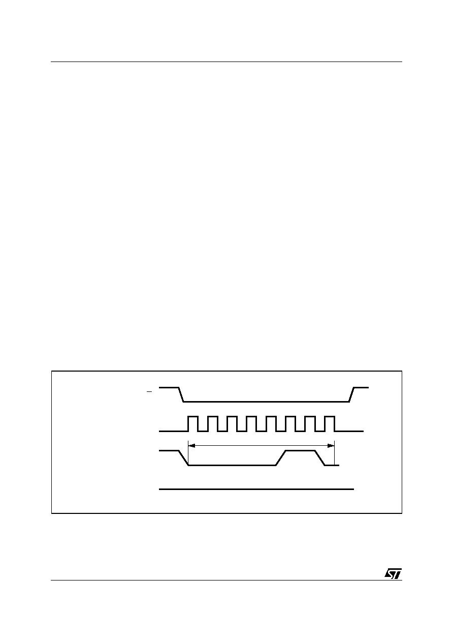
Figure 11. Write Enable Latch Sequence
00
01
02
03
04
HIGH IMPEDANCE
05
06
07
S
C
CPOL=0
CPHA=0
D
Q
D03AU1483

17/24
L5953
Figure 12. Test Mode Diagnostic Procedure Start (after a Write Enable Latch Sequence, Fig.11)
Figure 13. Read the Diagnostic registerCase1: after a Test Mode diagnostic procedure start (Fig.
12)
Figure 14. Diagnostic Procedure Start (after a Write Enable Latch Sequence, operation A)
Figure 15. Read the Diagnostic RegisterCase2: during the normal working of the L5953 (after a
Diagnostic Procedure Start, Fig.14)
00
01
02
03
04
HIGH IMPEDANCE
INSTRUCTION
STATUS REGISTER
05
06
07
08
09
10
11
12
13
14
15
16
17
18
19
20
21
22
23
s15
s14
s13
s12
s11
s10
s9
s8
s7
s6
s5
s4
s3
s2
s1
s0
S
C
D
Q
D03AU1484
CPOL=0, CPHA=0
00
01
02
03
04
HIGH IMPEDANCE
INSTRUCTION
DIAGNOSTIC REGISTER OUT
05
06
07
08
09
10
11
12
13
14
15
d7
d6
d5
d4
d3
d2
d1
d0
S
C
D
Q
D03AU1485
CPOL=0, CPHA=0
00
01
02
03
04
HIGH IMPEDANCE
INSTRUCTION
STATUS REGISTER
05
06
07
08
09
10
11
12
13
14
15
16
17
18
19
20
21
22
23
s15
s14
s13
s12
s11
s10
s9
s8
s7
s6
s5
s4
s3
s2
s1
s0
S
C
D
Q
D03AU1486
CPOL=0, CPHA=0
00
01
02
03
04
HIGH IMPEDANCE
INSTRUCTION
DIAGNOSTIC REGISTER OUT
05
06
07
08
09
10
11
12
13
14
15
d7
d6
d5
d4
d3
d2
d1
d0
S
C
D
Q
D03AU1487
CPOL=0, CPHA=0

L5953
18/24
Figure 16. Write the Status Register (after a Write Enable Latch Sequence, operation A)
Figure 17. Read the Status Register
IRQ - Interrupt Request Pin
s
It is an open drain pin activated (low) every time a variation occurs in the Diagnostic Register.
s
Purpose: to alert the
µ
P that one or more warning bit of the Diagnostic Register has changed from 0 to
1 or from 1 to 0.
s
An activation of this pin puts the bit s0 of the Status Register to 1 (START DIAGNOSTIC) like an
Operation E (Diagnostic Procedure Start). Then an Operation F has to be executed without an
Operation E before.
s
After an Operation F, the IRQ pin is disactivated, and goes to 1 if connected to a pull-up resistor.
L5953 - Application Note
00
01
02
03
04
HIGH IMPEDANCE
INSTRUCTION
STATUS REGISTER
05
06
07
08
09
10
11
12
13
14
15
16
17
18
19
20
21
22
23
s15
s14
s13
s12
s11
s10
s9
s8
s7
s6
s5
s4
s3
s2
s1
s0
S
C
D
Q
D03AU1488
CPOL=0, CPHA=0
00
01
02
03
04
HIGH IMPEDANCE
INSTRUCTION
STATUS REGISTER OUT
05
06
07
08
09
10
11
12
13
14
15
S
C
D
Q
D03AU1489
16
17
18
19
20
21
22
23
s15
s14
s13
s12
s11
s10
s9
s8
s7
s6
s5
s4
s3
s2
s1
s0
CPOL=0, CPHA=0

19/24
L5953
Figure 18. Block and Application Diagram
Figure 19. Block Diagram And Application With External Power MOS
VOLTAGE WARNING
SPI INTERFACE
REG2
LINEAR VOLTAGE
REGULATOR
1.5-3.3V/300mA
HSD1
HSD1
HSD2
C4
C3
D1
C6
HSD2
COMP
FB
GATEOUT
GATEIN
D2
R4
R5
R6
R3
C9
R2
R1
C8
VSW
DRAINOUT
STRAP
ADJ
VSTBY
GND
SWGND
S1
W1
S2
W2
VDD
Vo
VDD-LIN
REG1
ST-BY LINEAR VOLTAGE
REGULATOR
3.3-5V/250mA
PWM
STEP DOWN
REGULATOR
2.5-10V/1A
OSCILLATOR &
SYNC
STCAP
CT
RES
VDD-SW
IRQ
Q
D
S
C
VLR
FBLR
VIN
SYNC
DGND
FGND
D01AU1331B
L1
C1
C2
C5
C11
C10
C7
VSPI
VOLTAGE WARNING
SPI INTERFACE
REG2
LINEAR VOLTAGE
REGULATOR
1.5-3.3V/300mA
HSD1
HSD1
HSD2
C4
C3
D1
C6
HSD2
COMP
FB
GATEOUT
GATEIN
D2
M1
R4
R5
R6
R3
C9
R2
R1
C8
VSW
DRAINOUT
STRAP
ADJ
VSTBY
GND
SWGND
S1
W1
S2
W2
VDD
Vo
VDD-LIN
REG1
ST-BY LINEAR VOLTAGE
REGULATOR
3.3-5V/250mA
PWM
STEP DOWN
REGULATOR
2.5-10V/1A
OSCILLATOR &
SYNC
STCAP
CT
RES
VDD-SW
IRQ
Q
D
S
C
VLR
FBLR
VIN
SYNC
DGND
FGND
D01AU1332B
L1
C10
C7
VSPI
C2
C1
C5

L5953
20/24
PART LIST on Evaluation Board
REG1 OUTPUT VOLTAGE
V
STBY
= 5V if pin ADJ left floating
V
STBY
= 3.3V if pin ADJ is conneted to the pin V
STBY
Timing Capacitor
The value for this capacitor has to be chosen according the wanted power-on delay T
d
:
where I
CT1
is the source current used to charge the timing capacitor and V
STBY
is the REG1 output voltage.
Feedback resistors for REG2
where VLR is the required output voltage for REG2.
External components for PWM regulator
Bootstrap capacitor
The suggested value for the bootstrap capacitor is C6 = 100nF
Here following you find the criteria for the selection of the inductor L1, the free-wheeling diode D2, the output
filter capacitor C7, the feedback resistor R1, R2 and the compensation network R3, C8, R4, C9 to have a Buck
regulator working in Continuos mode. Continuous mode operation is recommended in order to reduce the stress
of the output capacitor and of the free-wheeling diode.
Inductor Selection
The minimum value of the inductor L7 has to be so that the maximum inductor current ripple
I
L,max
is 20% to
30% of the maximum load current load I
o,max
.The maximum ripple is present when the switching frequency is
minimum ( f
sw,min
) and the input voltage is maximum ( V
in,max
) so the minimum value for the inductor L
min
is :
Output Capacitor Selection
The criteria for the selection of the capacitor C7 is based on the output voltage ripple requirements. The ripple
on the output voltage is due to a capacitive contribute, often negligible, equal to
C1 = 470
µ
F
C2 = 220 nF
C3 = 470
µ
F
C4 = 10
µ
F
C5 = 1
µ
F
C6 = 100 nF
C7 = 470
µ
F
ESR=65 m
C8 = 56nF
C9 = 2.7 nF
C10 = 10
µ
F
C11 = 4.7 nF
R1 = 2.2 k
R2 = 2 x 1.5 k
in parallel
R3 = 10 k
R4 = 220 k
R5 = 3.3 k
R6 = 1 k
L1 = 180
µ
H
D1 = 1N4007 or
MBR160
D2 = MBR360
C11
I
CT 1
T
d
0.5 V
S TB Y
(
)
V
C TL Ry
+
--------------------------------------------------------------
=
R5
R6
V
LR
V
r ef R EG 2
,
--------------------------
1
≠
=
L
m in
V
O
I
L m ax
,
--------------------
1
V
O
V
i m ax
,
-----------------
1
f
s w m in
,
------------------
≠
=

21/24
L5953
and a resistive contribute given by the ESR of the capacitor and which is equal to
VC fixes the value for C7 while
VESR limits the ESR of the capacitor.Usually the capacitor is chosen so that
the total ripple on the output regulated voltage Vo is equal to 1% of the value of Vo. If V
ripple
is the maximum
allowed voltage ripple on Vo then it should result:
More often the minimum value of C7 is imposed by other considerations such as to get a good dynamic behav-
iour of the output voltage in case of large load variations.
Free-wheeling diode
The diode must withstand an average current Id equal to Id = I
lim
( 1- D
min
)
where I
lim
is the current of intervention of the short circuit protection and D
min
is the minimum duty cycle. As D
min
is vey low, the current Id can be assumed equal to I
lim
.
Compensation Network
In continuous mode, the voltage controlled buck converter showes two poles due to the output LC filter and one
zero due to the ESR of the output capacitor. The suggested compensation network introduces two zeros and
two poles:
≠ the zeros compensate the double poles of the LC filter
≠ one pole compensates the zero due to ESR of the output capacitor
≠ the second pole is nominally located in the origin which means an infinite gain at frequency null. In
the reality the DC value of the closed loop gain can not be greater than the DC value of the EA open
loop gain and the pole is located at very low frequency.
The values for the components of the compensation network can be fixed when the inductor L1 and the output
capacitor C7 are chosen.
The necessary steps are following:
1.fix the cross-over frequency f
C
of the overall loop gain.
Usually
where f
sw,min
is the minimum switching frequency
2.Calculate the high frequency error amplifier gain
3.Chose R3 and calculate
The value for R3 has not to be very high (for example 10K
) so to limit the error due to an error amplifier input
offset current.
V
c
I
L m ax
,
8 C7 f
s w m in
,
---------------------------------------
=
V
ESR
ESR
I
L m a x
,
=
V
ri ppl e
V
c
2
V
ES R
2
+
f
c
0.1 f
s w,min
=
G
c
0.25 f
c
2
L1
ESR
-------------
=
C8
2
L1 C7
R3
-----------------------
=

L5953
22/24
4.Calculate
5.Finally calculate
and
R
p
R3
2
E SR
-------------
L1
C7
--------
1
≠
---------------------------------------------
=
RA
R
p
V
O
V
ref PWM
,
-------------------------
=
R2
R
p
1
V
r ef,PWM
V
O
-----------------------
≠
---------------------------------
=
R4
G
C
R1
=
C9
2
L1 C7
R4
-----------------------
=
23/24
L5953
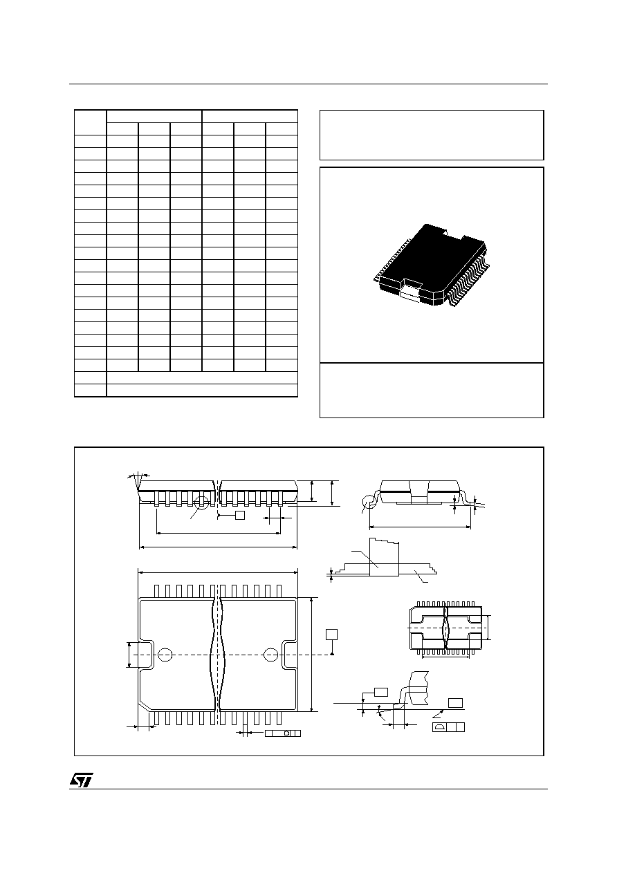
DIM.
mm
inch
MIN.
TYP.
MAX.
MIN.
TYP.
MAX.
A
3.60
0.141
a1
0.10
0.30
0.004
0.012
a2
3.30
0.130
a3
0
0.10
0
0.004
b
0.22
0.38
0.008
0.015
c
0.23
0.32
0.009
0.012
D (1)
15.80
16.00
0.622
0.630
D1
9.40
9.80
0.370
0.385
E
13.90
14.50
0.547
0.570
e
0.65
0.0256
e3
11.05
0.435
E1 (1)
10.90
11.10
0.429
0.437
E2
2.90
0.114
E3
5.80
6.20
0.228
0.244
E4
2.90
3.20
0.114
0.126
G
0
0.10
0
0.004
H
15.50
15.90
0.610
0.626
h
1.10
0.043
L
0.80
1.10
0.031
0.043
N
10
∞
(max.)
S
8
∞
(max.)
(1): "D" and "E1" do not include mold flash or protrusions
- Mold flash or protrusions shall not exceed 0.15mm (0.006 inch)
- Critical dimensions are "a3", "E" and "G".
PowerSO36
e
a2
A
E
a1
PSO36MEC
DETAIL A
D
1
1
8
19
36
E1
E2
h x 45∞
DETAIL A
lead
slug
a3
S
Gage Plane
0.35
L
DETAIL B
DETAIL B
(COPLANARITY)
G
C
- C -
SEATING PLANE
e3
c
N
N
M
0.12
A B
b
B
A
H
E3
D1
BOTTOM VIEW
OUTLINE AND
MECHANICAL DATA

Information furnished is believed to be accurate and reliable. However, STMicroelectronics assumes no responsibility for the consequences
of use of such information nor for any infringement of patents or other rights of third parties which may result from its use. No license is granted
by implication or otherwise under any patent or patent rights of STMicroelectronics. Specifications mentioned in this publication are subject
to change without notice. This publication supersedes and replaces all information previously supplied. STMicroelectronics products are not
authorized for use as critical components in life support devices or systems without express written approval of STMicroelectronics.
The ST logo is a registered trademark of STMicroelectronics.
All other names are the property of their respective owners
© 2003 STMicroelectronics - All rights reserved
STMicroelectronics GROUP OF COMPANIES
Australia - Belgium - Brazil - Canada - China - Czech Republic - Finland - France - Germany - Hong Kong - India - Israel - Italy - Japan -
Malaysia - Malta - Morocco - Singapore - Spain - Sweden - Switzerland - United Kingdom - United States
www.st.com
24/24
L5953