 | –≠–ª–µ–∫—Ç—Ä–æ–Ω–Ω—ã–π –∫–æ–º–ø–æ–Ω–µ–Ω—Ç: L5973A | –°–∫–∞—á–∞—Ç—å:  PDF PDF  ZIP ZIP |
1/13
L5973AD
September 2003
s
2A INTERNAL SWITCH
s
OPERATING INPUT VOLTAGE FROM 4.4V TO 36V
s
3.3V / (
±
2%) REFERENCE VOLTAGE
s
OUTPUT VOLTAGE ADJUSTABLE FROM
1.235V TO 35V
s
LOW DROPOUT OPERATION: 100% DUTY
CYCLE
s
500KHz INTERNALLY FIXED FREQUENCY
s
VOLTAGE FEEDFORWARD
s
ZERO LOAD CURRENT OPERATION
s
INTERNAL CURRENT LIMITING
s
INHIBIT FOR ZERO CURRENT
CONSUMPTION
s
SYNCHRONIZATION
s
PROTECTION AGAINST FEEDBACK
DISCONNECTION
s
THERMAL SHUTDOWN
APPLICATIONS:
s
CONSUMER: STB, DVD, TV, VCR,CAR
RADIO, LCD MONITORS
s
NETWORKING: XDSL, MODEMS,DC-DC
MODULES
s
COMPUTER: PRINTERS, AUDIO/GRAPHIC
CARDS, OPTICAL STORAGE, HARD DISK
DRIVE
s
INDUSTRIAL: CHARGERS, CAR BATTERY
DC-DC CONVERTERS
DESCRIPTION
The L5973AD is a step down monolithic power
switching regulator with a switch current limit of 2A so
it is able to deliver more than 1.5A DC current to the
load depending on the application conditions.
The output voltage can be set from 1.235V to 35V.
The high current level is also achieved thanks to an
SO8 package with exposed frame, that allows to re-
duce the R
th(j-amb)
down to approximately 40∞C/W
The device uses an internal P-Channel D-MOS tran-
sistor (with a typical of 200m
) as switching element
to avoid the use of bootstrap capacitor and guarantee
high efficiency.
An internal oscillator fixes the switching frequency at
500KHz to minimize the size of external components.
Having a minimum input voltage of 4.4V only, it is
particularly suitable for 5V bus, available in all com-
puter related applications.
Pulse by pulse current limit with the internal frequen-
cy modulation offers an effective constant current
short circuit protection.
HSOP8 - EXPOSED PAD
ORDERING NUMBERS: L5973AD (Tube)
L5973ADTR (Tape & Reel)
2A SWITCH STEP DOWN SWITCHING REGULATOR
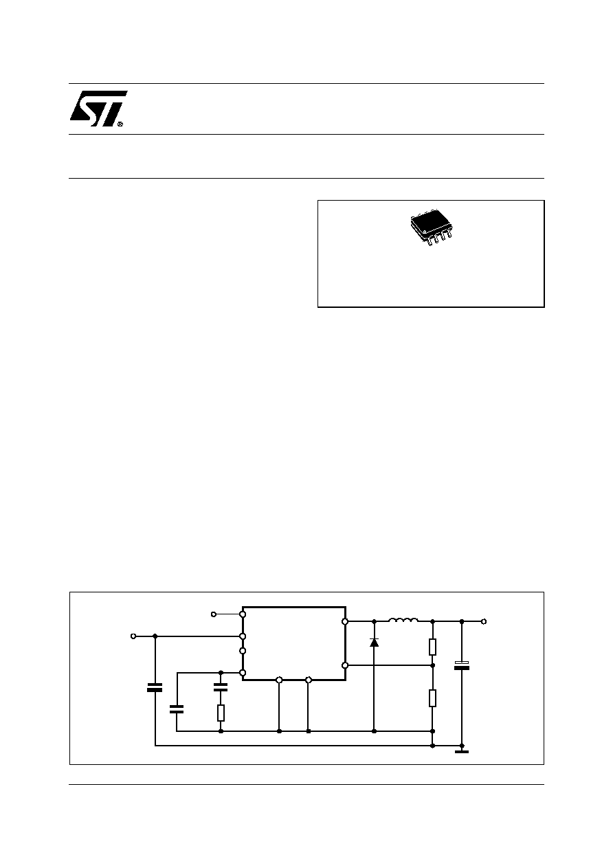
TEST APPLICATION CIRCUIT
D03IN1453
8
4
5
1
7
L5973AD
C1
10
µ
F
35V
CERAMIC
C2
330
µ
F
10V
VOUT=3.3V
VIN = 4.4V to 35V
R1
5.6K
R2
3.3K
R3
4.7K
C4
22nF
C3
220pF
3
L1 15
µ
H
D1
STPS340U
COMP
VCC
OUT
FB
GND
INH
2
6
3.3V
SYNC.
VREF

L5973AD
2/13
THERMAL DATA
(*) Package mounted on board
PIN CONNECTION
PIN DESCRIPTION
ABSOLUTE MAXIMUM RATINGS
Symbol
Parameter
Value
Unit
R
th (j-amb)
Thermal Resistance Junction to ambient
Max.
40 (*)
∞C/W
N.
Name
Description
1
OUT
Regulator Output.
2
SYNC
Master/Slave Synchronization. When it is open, a signal synchronous with the turn-off of the inter-
nal power is present at the pin. When connected to an external signal at a frequency higher than
the internal one, then the device is synchronized by the external signal.
Connecting together the SYNC pin of two devices, the one with the higher frequency works as
master and the other one, works as slave.
3
INH
A logical signal (active high) disables the device. With IHN higher than 2.2V the device is OFF and with
INH lower than 0.8V, the device is ON.
If INH is not used the pin must be grounded. When it is open, an internal pull-up disables the device.
4
COMP
E/A output to be used for frequency compensation.
5
FB
Stepdown feedback input. Connecting the output voltage directly to this pin results in an output
voltage of 1.235V. An external resistor divider is required for higher output voltages (the typical
value for the resistor connected between this pin and ground is 4.7K).
6
V
REF
Reference voltage of 3.3V. No filter capacitor is needed to stability.
7
GND
Ground.
8
V
CC
Unregulated DC input voltage.
Symbol
Parameter
Value
Unit
V
8
Input Voltage
40
V
V
1
Output DC voltage
Output peak voltage at t = 0.1
µ
s
-1 to 40
-5 to 40
V
V
I
1
Maximum output current
int. limit.
V
4
, V
5
Analog pins
4
V
V
3
INH
-0.3V to V
CC
V
2
SYNC
-0.3 to 4
V
P
tot
Power dissipation at T
amb
60∞C
2.25
W
T
j
Operating junction temperature range
-40 to 150
∞C
T
stg
Storage temperature range
-55 to 150
∞C
OUT
SYNC
INH
COMP
1
3
2
4
VCC
VREF
GND
FB
8
7
6
5
D98IN955

3/13
L5973AD
ELECTRICAL CHARACTERISTICS (T
j
= 25∞C, V
CC
= 12V, unless otherwise specified.)
Note: 1. Guaranteed by design
Symbol
Parameter
Test Condition
Min.
Typ.
Max.
Unit
V
CC
Operating input voltage range
V
o
= 1.235V; I
o
= 2A
4.4
36
V
R
DSON
Mosfet on Resistance
0.250
0.5
I
l
Maximum limiting current
V
CC
= 4.4V to 36V
2.3
A
f
s
Switching frequency
500
KHz
Duty cycle
0
100
%
DYNAMIC CHARACTERISTICS (see test circuit ).
V
5
Voltage feedback
4.4V < V
CC
< 36V
1.220
1.235
1.25
V
Efficiency
V
O
= 5V, V
CC
= 12V
90
%
DC CHARACTERISTICS
I
qop
Total Operating Quiescent Current
5
7
mA
I
q
Quiescent current
Duty Cycle = 0; V
FB
= 1.5V
2.7
mA
I
qst-by
Total stand-by quiescent current
V
inh
> 2.2V
50
100
µ
A
INHIBIT
INH Threshold Voltage
Device ON
0.8
V
Device OFF
2.2
V
ERROR AMPLIFIER
V
OH
High level output voltage
VFB = 1V
3.5
V
V
OL
Low level output voltage
VFB = 1.5V
0.4
V
I
o source
Source output current
V
COMP
= 1.9V; V
FB
= 1V
200
300
µ
A
I
o sink
Sink output current
V
COMP
= 1.9V; V
FB
= 1.5V
1
1.5
mA
I
b
Source bias current
2.5
4
µ
A
DC open loop gain
R
L
=
50
57
dB
gm
Transconductance
I
comp
= -0.1mA to 0.1mA
V
COMP
= 1.9V
2.3
mS
SYNC FUNCTION
High Input Voltage
V
CC
= 4.4V to 36V
2.5
V
REF
V
Low Input Voltage
V
CC
= 4.4V to 36V
0.74
V
Slave Sink Current
V
sync
= 0.74V
(1)
V
sync
= 2.33V
0.11
0.21
0.25
0.45
mA
mA
Master Output Amplitude
I
source
= 3mA
2.75
3
V
Output Pulse Width
no load, V
sync
= 1.65V
0.20
0.35
µ
s
REFERENCE SECTION
Reference Voltage
3.234
3.3
3.366
V
I
REF
= 0 to 5mA
V
CC
= 4.4V to 36V
3.2
3.3
3.399
V
Line Regulation
I
REF
= 0mA
V
CC
= 4.4V to 36V
5
10
mV
Load Regulation
I
REF
= 0 to 5mA
8
15
mV
Short Circuit Current
10
18
30
mA
L5973AD
4/13
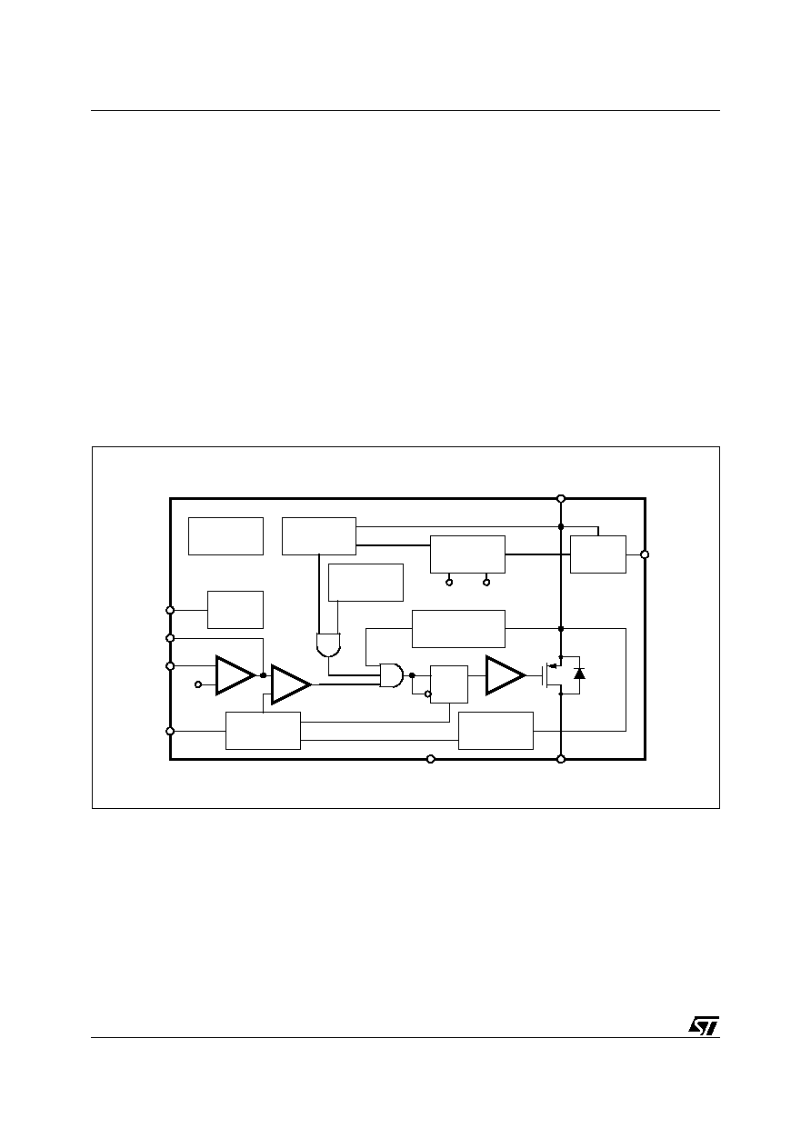
FUNCTIONAL DESCRIPTION
The main internal blocks are shown in Fig. 1, where is reported the device block diagram. They are:
s
A voltage regulator that supplies the internal circuitry. From this regulator, a 3.3V reference
voltage is externally available.
s
A voltage monitor circuit that checks the input and internal voltages.
s
A fully integrated sawtooth oscillator whose frequency is500KHz
s
Two embedded current limitations circuitries which control the current that flows through the
power switch. The Pulse by Pulse Current Limit forces the power switch OFF cycle by cycle
if the current reaches an internal threshold, while the Frequency Shifter reduces the switch-
ing frequency in order to strongly reduce the duty cycle.
s
A transconductance error amplifier.
s
A pulse width modulator (PWM) comparator and the relative logic circuitry necessary to drive
the internal power.
s
An high side driver for the internal P-MOS switch.
s
An inhibit block for stand-by operation.
s
A circuit to realize the thermal protection function.
Figure 1. Block Diagram
POWER SUPPLY & VOLTAGE REFERENCE
The internal regulator circuit (shown in Figure 2) consists of a start-up circuit, an internal voltage Prereg-
ulator, the Bandgap voltage reference and the Bias block that provides current to all the blocks.
The Starter gives the start-up currents to the whole device when the input voltage goes high and the de-
vice is enabled (inhibit pin connected to ground).
The Preregulator block supplies the Bandgap cell with a preregulated voltage V
REG
that has a very low
supply voltage noise sensitivity.
INHIBIT
VOLTAGES
MONITOR
PEAK TO PEAK
CURRENT LIMIT
THERMAL
SHUTDOWN
E/A
PWM
1.235V
+
-
-
+
OSCILLATOR
D
Ck
Q
FREQUENCY
SHIFTER
TRIMMING
SUPPLY
1.235V
3.5V
DRIVER
V
REF
BUFFER
LPDMOS
POWER
FB
SYNC
COMP
INH
VREF
GND
OUT
VCC
D00IN1125

5/13
L5973AD
VOLTAGES MONITOR
An internal block senses continuously the V
cc
, V
ref
and V
bg
. If the voltages go higher than their thresholds, the
regulator starts to work. There is also an hysteresis on the V
CC
(UVLO).
Figure 2. Internal Regulator Circuit
OSCILLATOR & SYNCHRONIZATOR
Figure 3 shows the block diagram of the oscillator circuit.
The Clock Generator provides the switching frequency of the device that is internally fixed at 500KHz. The frequency
shifter block acts reducing the switching frequency in case of strong overcurrent or short circuit. The clock signal is
then used in the internal logic circuitry and is the input of the Ramp Generator and Synchronizator blocks.
The Ramp Generator circuit provides the sawtooth signal, used to realize the PWM control and the internal volt-
age feed forward, while the Synchronizator circuit generates the synchronization signal. Infact the device has a
synchronization pin that can works both as Master and Slave.
As Master to synchronize external devices to the internal switching frequency.
As Slave to synchronize itself by external signal.
In particular, connecting together two devices, the one with the lower switching frequency works as Slave and
the other one works as Master.
To synchronize the device, the SYNC pin has to pass from a low level to a level higher than the synchronization
threshold with a duty cycle that can vary approximately from 10% to 90%, depending also on the signal frequen-
cy and amplitude.
The frequency of the synchronization signal must be at least higher than the internal switching frequency of the
device (500KHz).
STARTER
IC BIAS
PREREGULATOR
BANDGAP
VREG
VREF
D00IN1126
V
CC