 | –≠–ª–µ–∫—Ç—Ä–æ–Ω–Ω—ã–π –∫–æ–º–ø–æ–Ω–µ–Ω—Ç: L5973ADTR | –°–∫–∞—á–∞—Ç—å:  PDF PDF  ZIP ZIP |
1/14
L5973AD
December 2004
1
GENERAL FEATURES
2A INTERNAL SWITCH
OPERATING INPUT VOLTAGE FROM 4.4V TO 36V
3.3V / (
±2%) REFERENCE VOLTAGE
OUTPUT VOLTAGE ADJUSTABLE FROM
1.235V TO 35V
LOW DROPOUT OPERATION: 100% DUTY
CYCLE
500KHz INTERNALLY FIXED FREQUENCY
VOLTAGE FEEDFORWARD
ZERO LOAD CURRENT OPERATION
INTERNAL CURRENT LIMITING
INHIBIT FOR ZERO CURRENT
CONSUMPTION
SYNCHRONIZATION
PROTECTION AGAINST FEEDBACK
DISCONNECTION
THERMAL SHUTDOWN
1.1 APPLICATIONS:
CONSUMER: STB, DVD, TV, VCR,CAR
RADIO, LCD MONITORS
NETWORKING: XDSL, MODEMS,DC-DC
MODULES
COMPUTER: PRINTERS, AUDIO/GRAPHIC
CARDS, OPTICAL STORAGE, HARD DISK
DRIVE
INDUSTRIAL: CHARGERS, CAR BATTERY
DC-DC CONVERTERS
2
DESCRIPTION
The L5973AD is a step down monolithic power
switching regulator with a switch current limit of 2A so
it is able to deliver more than 1.5A DC current to the
load depending on the application conditions.
The output voltage can be set from 1.235V to 35V.
The high current level is also achieved thanks to an
SO8 package with exposed frame, that allows to re-
duce the R
th(j-amb)
down to approximately 40∞C/W
The device uses an internal P-Channel D-MOS tran-
sistor (with a typical of 200m
) as switching element
to avoid the use of bootstrap capacitor and guarantee
high efficiency.
An internal oscillator fixes the switching frequency at
500KHz to minimize the size of external components.
Having a minimum input voltage of 4.4V only, it is
particularly suitable for 5V bus, available in all com-
puter related applications.
Pulse by pulse current limit with the internal frequen-
cy modulation offers an effective constant current
short circuit protection.
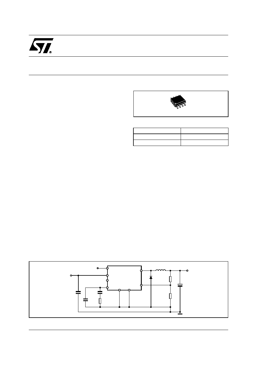
2A SWITCH STEP DOWN SWITCHING REGULATOR
Figure 2. Test and Application Circuit
D03IN1453
8
4
5
1
7
L5973AD
C1
10
µF
35V
CERAMIC
C2
330
µF
10V
VOUT=3.3V
VIN = 4.4V to 35V
R1
5.6K
R2
3.3K
R3
4.7K
C4
22nF
C3
220pF
3
L1 15
µH
D1
STPS340U
COMP
VCC
OUT
FB
GND
INH
2
6
3.3V
SYNC.
VREF
Figure 1. Package
Table 1. Order Codes
Part Number
Package
L5973AD
HSOP8
L5973ADTR
HSOP8 in Tape & Reel
HSOP8 (Exposed pad)
Rev. 3

L5973AD
2/14
Table 2. Thermal Data
(*) Package mounted on board
Figure 3. Pin Connection (top view)
Table 3. Pin Description
Table 4. Absolute Maximum Ratings
Symbol
Parameter
Value
Unit
R
th (j-amb)
Thermal Resistance Junction to ambient
Max.
40 (*)
∞C/W
N.
Name
Description
1
OUT
Regulator Output.
2
SYNC
Master/Slave Synchronization. When it is open, a signal synchronous with the turn-off of the inter-
nal power is present at the pin. When connected to an external signal at a frequency higher than
the internal one, then the device is synchronized by the external signal.
Connecting together the SYNC pin of two devices, the one with the higher frequency works as
master and the other one, works as slave.
3
INH
A logical signal (active high) disables the device. With IHN higher than 2.2V the device is OFF and with
INH lower than 0.8V, the device is ON.
If INH is not used the pin must be grounded. When it is open, an internal pull-up disables the device.
4
COMP
E/A output to be used for frequency compensation.
5
FB
Stepdown feedback input. Connecting the output voltage directly to this pin results in an output
voltage of 1.235V. An external resistor divider is required for higher output voltages (the typical
value for the resistor connected between this pin and ground is 4.7K).
6
V
REF
Reference voltage of 3.3V. No filter capacitor is needed to stability.
7
GND
Ground.
8
V
CC
Unregulated DC input voltage.
Symbol
Parameter
Value
Unit
V
8
Input Voltage
40
V
V
1
Output DC voltage
Output peak voltage at t = 0.1
µs
-1 to 40
-5 to 40
V
V
I
1
Maximum output current
int. limit.
V
4
, V
5
Analog pins
4
V
V
3
INH
-0.3V to V
CC
V
2
SYNC
-0.3 to 4
V
P
tot
Power dissipation at T
amb
60∞C
2.25
W
T
j
Operating junction temperature range
-40 to 150
∞C
T
stg
Storage temperature range
-55 to 150
∞C
OUT
SYNC
INH
COMP
1
3
2
4
VCC
VREF
GND
FB
8
7
6
5
D98IN955
3/14
L5973AD
Table 5. Electrical Characteristics (T
j
= 25∞C, V
CC
= 12V, unless otherwise specified.)
Note:
1. Guaranteed by design
Symbol
Parameter
Test Condition
Min.
Typ.
Max.
Unit
V
CC
Operating input voltage range
V
o
= 1.235V; I
o
= 2A
4.4
36
V
R
DSON
Mosfet on Resistance
0.250
0.5
I
l
Maximum limiting current
V
CC
= 4.4V to 36V
2
2.3
A
f
s
Switching frequency
500
KHz
Duty cycle
0
100
%
DYNAMIC CHARACTERISTICS (see test circuit ).
V
5
Voltage feedback
4.4V < V
CC
< 36V
1.220
1.235
1.25
V
Efficiency
V
O
= 5V, V
CC
= 12V
90
%
DC CHARACTERISTICS
I
qop
Total Operating Quiescent Current
5
7
mA
I
q
Quiescent current
Duty Cycle = 0; V
FB
= 1.5V
2.7
mA
I
qst-by
Total stand-by quiescent current
V
inh
> 2.2V
50
100
µA
INHIBIT
INH Threshold Voltage
Device ON
0.8
V
Device OFF
2.2
V
ERROR AMPLIFIER
V
OH
High level output voltage
VFB = 1V
3.5
V
V
OL
Low level output voltage
VFB = 1.5V
0.4
V
I
o source
Source output current
V
COMP
= 1.9V; V
FB
= 1V
200
300
µA
I
o sink
Sink output current
V
COMP
= 1.9V; V
FB
= 1.5V
1
1.5
mA
I
b
Source bias current
2.5
4
µA
DC open loop gain
R
L
=
50
57
dB
gm
Transconductance
I
comp
= -0.1mA to 0.1mA
V
COMP
= 1.9V
2.3
mS
SYNC FUNCTION
High Input Voltage
V
CC
= 4.4V to 36V
2.5
V
REF
V
Low Input Voltage
V
CC
= 4.4V to 36V
0.74
V
Slave Sink Current
V
sync
= 0.74V
(1)
V
sync
= 2.33V
0.11
0.21
0.25
0.45
mA
mA
Master Output Amplitude
I
source
= 3mA
2.75
3
V
Output Pulse Width
no load, V
sync
= 1.65V
0.20
0.35
µs
REFERENCE SECTION
Reference Voltage
3.234
3.3
3.366
V
I
REF
= 0 to 5mA
V
CC
= 4.4V to 36V
3.2
3.3
3.399
V
Line Regulation
I
REF
= 0mA
V
CC
= 4.4V to 36V
5
10
mV
Load Regulation
I
REF
= 0 to 5mA
8
15
mV
Short Circuit Current
10
18
30
mA
L5973AD
4/14
3
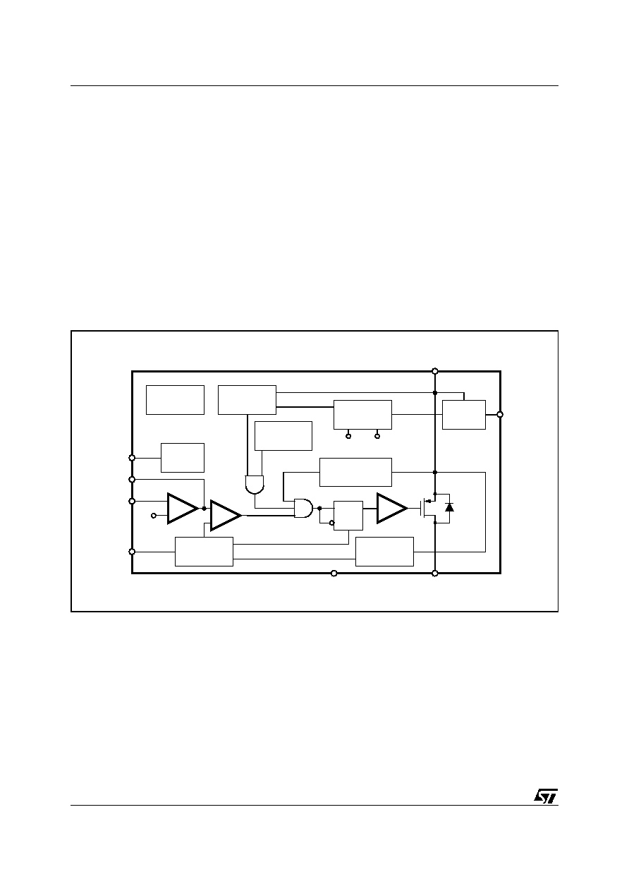
FUNCTIONAL DESCRIPTION
The main internal blocks are shown in Fig. 1, where is reported the device block diagram. They are:
A voltage regulator that supplies the internal circuitry. From this regulator, a 3.3V reference
voltage is externally available.
A voltage monitor circuit that checks the input and internal voltages.
A fully integrated sawtooth oscillator whose frequency is500KHz
Two embedded current limitations circuitries which control the current that flows through the
power switch. The Pulse by Pulse Current Limit forces the power switch OFF cycle by cycle
if the current reaches an internal threshold, while the Frequency Shifter reduces the switch-
ing frequency in order to strongly reduce the duty cycle.
A transconductance error amplifier.
A pulse width modulator (PWM) comparator and the relative logic circuitry necessary to drive
the internal power.
An high side driver for the internal P-MOS switch.
An inhibit block for stand-by operation.
A circuit to realize the thermal protection function.
Figure 4. Block Diagram
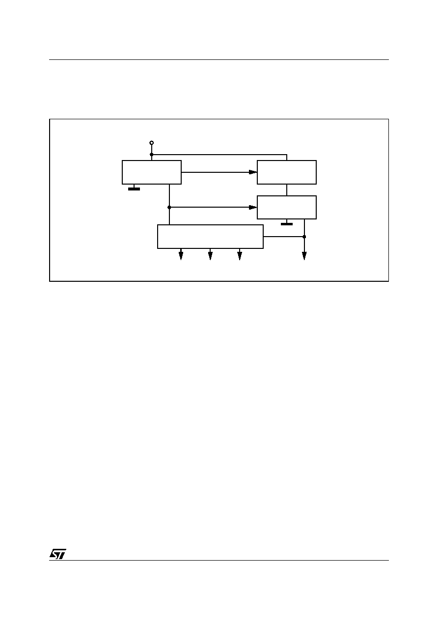
3.1 POWER SUPPLY & VOLTAGE REFERENCE
The internal regulator circuit (shown in Figure 2) consists of a start-up circuit, an internal voltage Prereg-
ulator, the Bandgap voltage reference and the Bias block that provides current to all the blocks.
The Starter gives the start-up currents to the whole device when the input voltage goes high and the de-
vice is enabled (inhibit pin connected to ground).
The Preregulator block supplies the Bandgap cell with a preregulated voltage V
REG
that has a very low
supply voltage noise sensitivity.
INHIBIT
VOLTAGES
MONITOR
PEAK TO PEAK
CURRENT LIMIT
THERMAL
SHUTDOWN
E/A
PWM
1.235V
+
-
-
+
OSCILLATOR
D
Ck
Q
FREQUENCY
SHIFTER
TRIMMING
SUPPLY
1.235V
3.5V
DRIVER
V
REF
BUFFER
LPDMOS
POWER
FB
SYNC
COMP
INH
VREF
GND
OUT
VCC
D00IN1125
5/14
L5973AD
3.2 VOLTAGES MONITOR
An internal block senses continuously the V
cc
, V
ref
and V
bg
. If the voltages go higher than their thresholds, the
regulator starts to work. There is also an hysteresis on the V
CC
(UVLO).
Figure 5. Internal Regulator Circuit
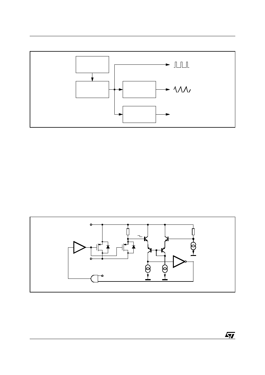
3.3 OSCILLATOR & SYNCHRONIZATOR
Figure 6 shows the block diagram of the oscillator circuit.
The Clock Generator provides the switching frequency of the device that is internally fixed at 500KHz. The frequency
shifter block acts reducing the switching frequency in case of strong overcurrent or short circuit. The clock signal is
then used in the internal logic circuitry and is the input of the Ramp Generator and Synchronizator blocks.
The Ramp Generator circuit provides the sawtooth signal, used to realize the PWM control and the internal volt-
age feed forward, while the Synchronizator circuit generates the synchronization signal. Infact the device has a
synchronization pin that can works both as Master and Slave.
As Master to synchronize external devices to the internal switching frequency.
As Slave to synchronize itself by external signal.
In particular, connecting together two devices, the one with the lower switching frequency works as Slave and
the other one works as Master.
To synchronize the device, the SYNC pin has to pass from a low level to a level higher than the synchronization
threshold with a duty cycle that can vary approximately from 10% to 90%, depending also on the signal frequen-
cy and amplitude.
The frequency of the synchronization signal must be at least higher than the internal switching frequency of the
device (500KHz).
STARTER
IC BIAS
PREREGULATOR
BANDGAP
VREG
VREF
D00IN1126
V
CC
L5973AD
6/14
Figure 6. Oscillator Circuit
3.4 CURRENT PROTECTION
The L5973AD has two current limit protections, pulse by pulse and frequency fold back.
The schematic of the current limitation circuitry for the pulse by pulse protection is shown in figure 7.
The output power PDMOS transistor is split in two parallel PDMOS. The smallest one has a resistor in series,
R
SENSE
. The current is sensed through Rsense and if reaches the threshold, the mirror is unbalanced and the
PDMOS is switched off until the next falling edge of the internal clock pulse.
Due to this reduction of the ON time, the output voltage decreases.
Since the minimum switch ON time (necessary to avoid false overcurrent signal) is not enough to obtain a suf-
ficiently low duty cycle at 500KHz, the output current, in strong overcurrent or short circuit conditions, could in-
crease again. For this reason the switching frequency is also reduced, so keeping the inductor current under its
maximum threshold. The Frequency Shifter (see fig. 6) depends on the feedback voltage. As the feedback volt-
age decreases (due to the reduced duty cycle), the switching frequency decreases too.
Figure 7. Current Limitation Circuitry
FREQUENCY
SHIFTER
CLOCK
GENERATOR
RAMP
GENERATOR
SYNCHRONIZATOR
CLOCK
RAMP
Ibias_osc
SYNC
t
D00IN1131
DRIVER
NOT
A1
PWM
VCC
OUT
A1/A2=95
I
L
RSENSE
D00IN1134
I
OFF
I
I
RTH
A2
7/14
L5973AD
3.5 ERROR AMPLIFIER
The voltage error amplifier is the core of the loop regulation. It is a transconductance operational amplifier whose
non inverting input is connected to the internal voltage reference (1.235V), while the inverting input (FB) is con-
nected to the external divider or directly to the output voltage. The output (COMP) is connected to the external
compensation network.
The uncompensated error amplifier has the following characteristics:
The error amplifier output is compared with the oscillator sawtooth to perform PWM control.
3.6 PWM COMPARATOR AND POWER STAGE
This block compares the oscillator sawtooth and the error amplifier output signals generating the PWM
signal for the driving stage.
The power stage is a very critical block cause it has to guarantee a correct turn on and turn off of the PD-
MOS.
The turn on of the power element, or better, the rise time of the current at turn on, is a very critical param-
eter to compromise.
At a first approach, it looks like the faster it is the rise time, the lower are the turn on losses.
But there is a limit introduced by the recovery time of the recirculation diode.
In fact when the current of the power element equals the inductor current, the diode turns off and the drain
of the power is free to go high. But during its recovery time, the diode can be considered as an high value
capacitor and this produces a very high peak current, responsible of many problems:
Spikes on the device supply voltage that cause oscillations (and thus noise) due to the board parasitics.
Turn on overcurrent causing a decrease of the efficiency and system reliability.
Big EMI problems.
Shorter freewheeling diode life.
The fall time of the current during the turn off is also critical. In fact it produces voltage spikes (due to the
parasitics elements of the board) that increase the voltage drop across the PDMOS.
In order to minimize all these problems, a new topology of driving circuit has been used and its block dia-
gram is shown in fig. 8.
The basic idea is to change the current levels used to turn on and off the power switch, according with the
PDMOS status and with the gate clamp status.
This circuitry allow to turn off and on quickly the power switch and to manage the above question related
to the freewheeling diode recovery time problem. The gate clamp is necessary to avoid that Vgs of the
internal switch goes higher than Vgsmax. The ON/OFF Control block avoids any cross conduction be-
tween the supply line and ground.
Transconductance
2300
µS
Low frequency gain
65dB
Minimum sink/source voltage
1500
µA/300µA
Output voltage swing
0.4V/3.65V
Input bias current
2.5
µA

L5973AD
8/14
Figure 8. Driving Circuitry
3.7 INHIBIT FUNCTION
The inhibit feature allows to put in stand-by mode the device. With INH pin higher than 2.2V the device is dis-
abled and the power consumption is reduced to less than 100
µA. With INH pin lower than 0.8V, the device is
enabled. If the INH pin is left floating, an internal pull up ensures that the voltage at the pin reaches the inhibit
threshold and the device is disabled. The pin is also Vcc compatible.
3.8 THERMAL SHUTDOWN
The shutdown block generates a signal that turns off the power stage if the temperature of the chip goes higher
than a fixed internal threshold (150∞C). The sensing element of the chip is very close to the PDMOS area, so
ensuring an accurate and fast temperature detection. An hysteresis of approximately 20∞C avoids that the de-
vices turns on and off continuously
4
ADDITIONAL FEATURES AND PROTECTIONS
4.1 FEEDBACK DISCONNECTION
In case of feedback disconnection, the duty cycle increases versus the maximum allowed value, bringing the
output voltage close to the input supply. This condition could destroy the load.
To avoid this dangerous condition, the device is turned off if the feedback pin remains floating.
4.2 OUTPUT OVERVOLTAGE PROTECTION
The overvoltage protection, OVP, is realized by using an internal comparator, which input is connected to the
feedback, that turns off the power stage when the OVP threshold is reached. This threshold is typically 30%
higher than the feedback voltage.
When a voltage divider is requested for adjusting the output voltage (see test application circuit), the OVP inter-
vention will be set at:
Where R
1
is the resistor connected between the output voltage and the feedback pin, while R
2
is between the
feedback pin and ground.
Vgsmax
GATE
STOP
DRIVE
DRAIN
OFF
ON
PDMOS
VOUT
DRAIN
VCC
I
LOAD
C
ESR
D00IN1133
I
OFF
I
ON
ON/OFF
CONTROL
CLAMP
L
V
OVP
1.3
R
1
R
2
+
R
2
-------------------- V
FB
=
9/14
L5973AD
4.3 ZERO LOAD
Due to the fact that the internal power is a PDMOS, no boostrap capacitor is required and so, the device works prop-
erly also with no load at the output. In this condition it works in burst mode, with random repetition rate of the burst.
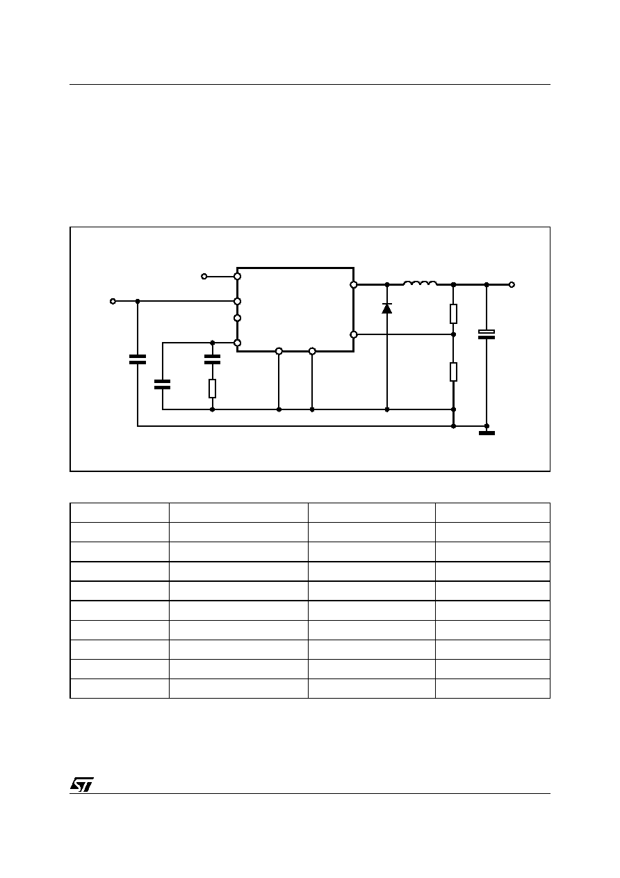
4.4 APPLICATION CIRCUIT
In figure 9 is shown the demo board application circuit, where the input supply voltage, V
cc
, can range from 4.4V
to 25V due to the rated voltage of the input capacitor and the output voltage is adjustable from 1.235V to V
cc
.
Figure 9. Demo board Application Circuit
Table 6. Component List
Reference
Part Number
Description
Manufacturer
C1
10
µF, 25V
TOKIN
C2
POSCAP 6TPB330M
330
µF, 6.3V
Sanyo
C3
C1206C221J5GAC
220pF, 5%, 50V
KEMET
C4
C1206C223K5RAC
22nF, 10%, 50V
KEMET
R1
5.6K, 1%, 0.1W 0603
Neohm
R2
3.3K, 1%, 0.1W 0603
Neohm
R3
4.7K, 1%, 0.1W 0603
Neohm
D1
STPS2L25U
2A, 25V
ST
L1
DO3316P-153
15
µH, 3A
COILCRAFT
D03IN1454
8
4
5
1
7
L5973AD
C1
10
µF
25V
CERAMIC
C2
330
µF
6.3V
VOUT=3.3V
VIN = 4.4V to 25V
R1
5.6K
R2
3.3K
R3
4.7K
C4
22nF
C3
220pF
3
L1 15
µH
D1
STPS2L25U
COMP
VCC
OUT
FB
GND
INH
2
6
3.3V
SYNC.
VREF
L5973AD
10/14
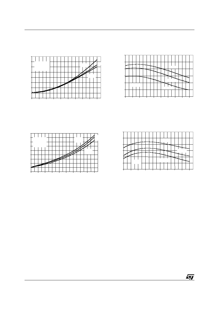
Figure 10. Junction Temperature vs. Output
Current
Figure 11. Junction Temperature vs Output
Current
Figure 12. Efficiency vs. Output Current
Figure 13. Efficiency vs. Output Current
20
30
40
50
60
70
80
90
100
0.2
0.4
0.6
0.8
1
1.2
1.4
1.6
1.8
2
Io(A)
Tj(∞C)
Vo=2.5V
Vo=3.3V
Vo=1.8V
Vin=5V
Tamb=25∞C
20
30
40
50
60
70
80
90
100
0.2
0.4
0.6
0.8
1
1.2
1.4
1.6
1.8
2
Io(A)
Tj(∞C)
Vo=2.5V
Vo=3.3V
Vo=1.8V
Vin=5V
Tamb=25∞C
20
30
40
50
60
70
80
90
100
110
0.2
0.4
0.6
0.8
1
1.2
1.4
1.6
1.8
2
Io(A)
Tj(C)
Vin=12V
Tamb=25∞C
Vo=3.3V
Vo=5V
Vo=2.5V
20
30
40
50
60
70
80
90
100
110
0.2
0.4
0.6
0.8
1
1.2
1.4
1.6
1.8
2
Io(A)
Tj(C)
Vin=12V
Tamb=25∞C
Vo=3.3V
Vo=5V
Vo=2.5V
65
70
75
80
85
90
95
0.2
0.4
0.6
0.8
1
1.2
1.4
1.6
1.8
2
Io(A)
E
ffi
c
i
e
n
c
y
(%
)
Vin=5V
Vout=2.5V
Vout=3.3V
Vout=1.8V
65
70
75
80
85
90
95
0.2
0.4
0.6
0.8
1
1.2
1.4
1.6
1.8
2
Io(A)
E
ffi
c
i
e
n
c
y
(%
)
Vin=5V
Vout=2.5V
Vout=3.3V
Vout=1.8V
65
70
75
80
85
90
95
0.2
0.4
0.6
0.8
1
1.2
1.4
1.6
1.8
2
Io(A)
E
ffi
ci
en
c
y
(%
)
Vin=12V
Vout=3.3V
Vout=2.5V
Vout=5V
65
70
75
80
85
90
95
0.2
0.4
0.6
0.8
1
1.2
1.4
1.6
1.8
2
Io(A)
E
ffi
ci
en
c
y
(%
)
Vin=12V
Vout=3.3V
Vout=2.5V
Vout=5V
11/14
L5973AD
5
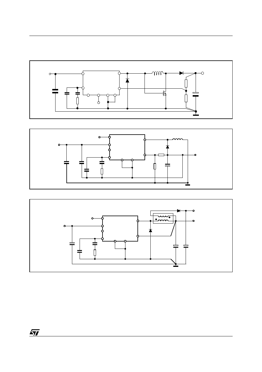
APPLICATION IDEAS
Figure 14. Positive Buck-Boost regulator
Figure 15. Buck-Boost regulator
Figure 16. Dual output voltage with auxiliary winding
Refer to L5973AD application note (AN1723) to have additional information, details, and more application
ideas.
L5973AD belongs to L597x family.
Related part numbers are:
L5970D: 1.5A (I
sw
), 250KHz Step Down DC-DC Converter in SO8
L5972D: 2A (I
sw
), 250KHz Step Down DC-DC Converter in SO8
L5973D: 2.5A (I
sw
), 250KHz Step Down DC-DC Converter in HSOP8
In case higher current is needed, the nearest DC-DC Converter family is L497x.
VIN=5V
C1
10uF
10V
Ceramic
D1
STPS2L25U
Vcc
COMP
GND
OUT
FB
INH
SYNC
VREF
L5973AD
1
3
7
5
6
4
8
2
R3
4.7k
L1
15uH
24k
2.7k
C3
22nF
3.3V
C4
100uF
16V
VOUT=12V/0.6A
C2
220pF
D2
STPS2L25U
M1
STN4NE03L
D03IN1455
8
4
5
1
7
L5973AD
C1
10
µF
10V
CERAMIC
C2
10
µF
25V
CERAMIC
C5
100
µF
16V
VOUT=-12V/
0.6A
VIN = 5V
2.7K
24K
R3
4.7K
C4
22nF
C3
220pF
3
L1 15
µH
D1
STPS2L25U
COMP
VCC
OUT
FB
GND
INH
2
6
3.3V
SYNC.
VREF
D03IN1456
8
4
5
1
7
L5973AD
C1
10
µF
25V
CERAMIC
C5
47
µF
10V
C4
100
µF
10V
VOUT=3.3V/
0.5A
VOUT1=5V/
50mA
VIN = 5V
R3
4.7K
C3
22nF
C2
220pF
3
Lp 22
µH
N1/N2=2
D1
STPS25L25U
D2
1N4148
COMP
VCC
OUT
FB
GND
INH
2
6
3.3V
SYNC.
VREF

L5973AD
12/14
6
PACKAGE INFORMATION
Figure 17. HSOP8 (Exposed Pad) Mechanical Data & Package Dimensions
OUTLINE AND
MECHANICAL DATA
DIM.
mm
inch
MIN.
TYP.
MAX.
MIN.
TYP.
MAX.
A
1.350
1.750
0.531
0.069
0.100
0.250
0.004
0.010
1.100
1.650
0.043
0.065
0.330
0.510
0.013
0.020
0.190
0.250
0.07
0.010
4.800
5.000
0.189
0.197
3.800
4.000
0.150
0.157
1.270
0.05
5.800
6.200
0.228
0.244
0.250
0.500
0.010
0.020
0.400
1.270
0.016
0.05
k
0∞ (min), 8∞ (max)
ddd
0.100
0.010
(1) Dimension D does not include mold flash, protusions
or gate burrs shall not exeed 0.15mm (both side).
HSOP8
7195016
(Exposed Pad)
A1
A2
B
C
D
E
e
H
h
L
Exposed Pad:
D1 = 3.1mm
E1 = 2.41mm

13/14
L5973AD
7
REVISION HISTORY
Table 7. Revision History
Date
Revision
Description of Changes
December 2003
1
First Issue
January 2004
2
Migration to EDOCS dms
December 2004
3
Added D1 & E1 dimensions in HSOP8 package information.

Information furnished is believed to be accurate and reliable. However, STMicroelectronics assumes no responsibility for the consequences
of use of such information nor for any infringement of patents or other rights of third parties which may result from its use. No license is granted
by implication or otherwise under any patent or patent rights of STMicroelectronics. Specifications mentioned in this publication are subject
to change without notice. This publication supersedes and replaces all information previously supplied. STMicroelectronics products are not
authorized for use as critical components in life support devices or systems without express written approval of STMicroelectronics.
The ST logo is a registered trademark of STMicroelectronics.
All other names are the property of their respective owners
© 2004 STMicroelectronics - All rights reserved
STMicroelectronics group of companies
Australia - Belgium - Brazil - Canada - China - Czech Republic - Finland - France - Germany - Hong Kong - India - Israel - Italy - Japan -
Malaysia - Malta - Morocco - Singapore - Spain - Sweden - Switzerland - United Kingdom - United States of America
www.st.com
14/14
L5973AD