1/10
L5973D
September 2003
s
2.5A INTERNAL SWITCH
s
OPERATING INPUT VOLTAGE FROM 4.4V TO 36V
s
3.3V / (
±
2%) REFERENCE VOLTAGE
s
OUTPUT VOLTAGE ADJUSTABLE FROM
1.235V TO 35V
s
LOW DROPOUT OPERATION: 100% DUTY
CYCLE
s
250KHz INTERNALLY FIXED FREQUENCY
s
VOLTAGE FEEDFORWARD
s
ZERO LOAD CURRENT OPERATION
s
INTERNAL CURRENT LIMITING
s
INHIBIT FOR ZERO CURRENT
CONSUMPTION
s
SYNCHRONIZATION
s
PROTECTION AGAINST FEEDBACK
DISCONNECTION
s
THERMAL SHUTDOWN
APPLICATIONS:
s
CONSUMER: STB, DVD, TV, VCR,CAR
RADIO, LCD MONITORS
s
NETWORKING: XDSL, MODEMS,DC-DC
MODULES
s
COMPUTER: PRINTERS, AUDIO/GRAPHIC
CARDS, OPTICAL STORAGE, HARD DISK
DRIVE
s
INDUSTRIAL: CHARGERS, CAR BATTERY
DC-DC CONVERTERS
DESCRIPTION
The L5973D is a step down monolithic power switch-
ing regulator with a minimum switch current limit of
2.5A so it is able to deliver more than 2A DC current
to the load depending on the application conditions.
The output voltage can be set from 1.235V to 35V.
The high current level is also achieved thanks to an
SO8 package with exposed frame, that allows to re-
duce the R
th(j-amb)
down to approximately 40∞C/W
The device uses an internal P-Channel D-MOS tran-
sistor (with a typical Rdson of 250m
) as switching
element to minimize the size of the external compo-
nents.
An internal oscillator fixes the switching frequency at
250KHz.
Having a minimum input voltage of 4.4V only, it is
particularly suitable for 5V bus, available in all com-
puter related applications.
Pulse by pulse current limit with the internal frequen-
cy modulation offers an effective constant current
short circuit protection.
HSOP8 - EXPOSED PAD
ORDERING NUMBERS: L5973D (Tube)
L5973D013TR (T & R)
2.5A SWITCH STEP DOWN SWITCHING REGULATOR
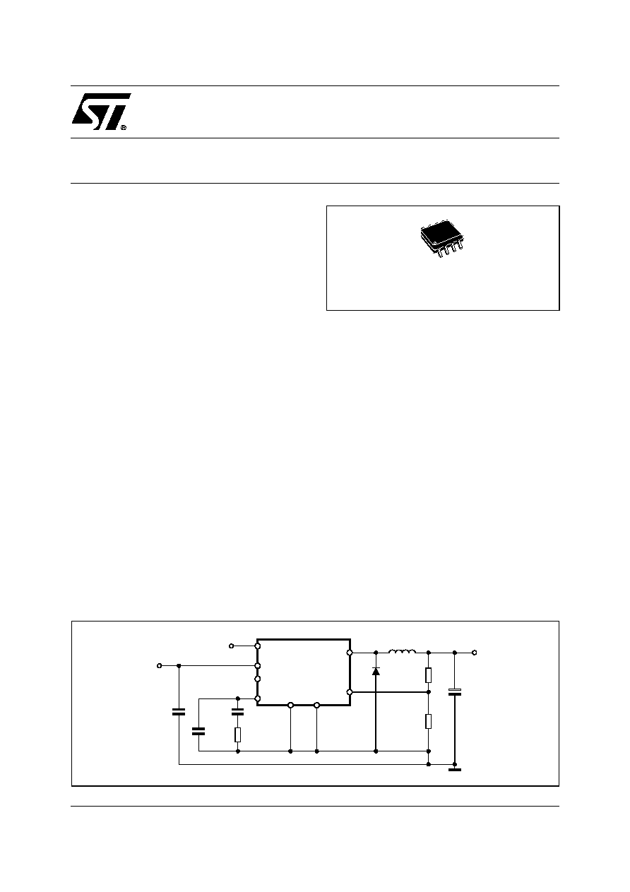
TEST APPLICATION CIRCUIT
D03IN1439
8
4
5
1
7
L5973D
C1
10
µ
F
35V
CERAMIC
C2
330
µ
F
10V
VOUT=3.3V
VIN = 4.4V to 35V
R1
5.6K
R2
3.3K
R3
4.7K
C4
22nF
C3
220pF
3
L1 15
µ
H
D1
STPS340U
COMP
VCC
OUT
FB
GND
INH
2
6
3.3V
SYNC.
VREF

L5973D
2/10
PIN CONNECTION
PIN DESCRIPTION
THERMAL DATA
(*) Package mounted on board
ABSOLUTE MAXIMUM RATINGS
N∞
Pin
Function
1
OUT
Regulator Output.
2
SYNC
Master/slave synchronization.
3
INH
A logical signal (active high) disables the device. If INH not used the pin must be grounded.
When it is open an internal pull-up disable the device.
4
COMP
E/A output for frequency compensation.
5
FB
Feedback input. Connecting directly to this pin results in an output voltage of 1.23V. An external
resistive divider is required for higher output voltages.
6
VREF
3.3V V
REF
. No cap is requested for stability.
7
GND
Ground.
8
VCC
Unregulated DC input voltage.
Symbol
Parameter
Value
Unit
R
th (j-amb)
Thermal Resistance Junction to ambient
Max.
40 (*)
∞C/W
Symbol
Parameter
Value
Unit
V
8
Input Voltage
40
V
V
1
Output DC voltage
Output peak voltage at t = 0.1
µ
s
-1 to 40
-5 to 40
V
V
I
1
Maximum output current
int. limit.
V
4
, V
5
Analog pins
4
V
V
3
INH
-0.3V to V
CC
V
2
SYNC
-0.3 to 4
V
P
tot
Power dissipation at T
amb
60∞C
2.25
W
T
j
Operating junction temperature range
-40 to 150
∞C
T
stg
Storage temperature range
-55 to 150
∞C
OUT
SYNC
INH
COMP
1
3
2
4
VCC
VREF
GND
FB
8
7
6
5
D98IN955

3/10
L5973D
ELECTRICAL CHARACTERISTICS (T
j
= 25∞C, V
CC
= 12V, unless otherwise specified.)
(*) Specification Referred to Tj from -40 to 125∞C
(1)
.
Notes: 1. Specification over the -40 to +125 Tj Temperature range are assured by design, characterization and statistical correlation.
2. Guaranteed by design.
Symbol
Parameter
Test Condition
Min.
Typ.
Max.
Unit
V
CC
Operating input voltage range
V
o
= 1.235V; I
o
= 2A
*
4.4
36
V
R
DSON
Mosfet on Resistance
*
0.250
0.5
I
l
Maximum limiting current
V
CC
= 4.4V to 36V
2.5
3
3.5
A
f
s
Switching frequency
*
212
250
280
KHz
225
250
275
KHz
Duty cycle
0
100
%
DYNAMIC CHARACTERISTICS (see test circuit ).
V
5
Voltage feedback
4.4V < V
CC
< 36V,
20mA < I
O
< 2A
1.220
1.235
1.25
V
*
1.198
1.235
1.272
V
Efficiency
V
O
= 5V, V
CC
= 12V
90
%
DC CHARACTERISTICS
I
qop
Total Operating Quiescent
Current
*
3
5
mA
I
q
Quiescent current
Duty Cycle = 0; V
FB
= 1.5V
2.5
mA
I
qst-by
Total stand-by quiescent current
V
inh
> 2.2V
*
50
100
µ
A
V
CC
= 36V; V
inh
> 2.2V
*
80
150
µ
A
INHIBIT
INH Threshold Voltage
Device ON
0.8
V
Device OFF
2.2
V
ERROR AMPLIFIER
V
OH
High level output voltage
VFB = 1V
3.5
V
V
OL
Low level output voltage
VFB = 1.5V
0.4
V
I
o source
Source output current
V
COMP
= 1.9V; V
FB
= 1V
200
300
µ
A
I
o sink
Sink output current
V
COMP
= 1.9V; V
FB
= 1.5V
1
1.5
mA
I
b
Source bias current
2.5
4
µ
A
DC open loop gain
R
L
=
50
57
dB
gm
Transconductance
I
comp
= -0.1mA to 0.1mA
V
COMP
= 1.9V
2.3
mS
SYNC FUNCTION
High Input Voltage
V
CC
= 4.4V to 36V
2.5
V
REF
V
Low Input Voltage
V
CC
= 4.4V to 36V
0.74
V
Slave Sink Current
V
sync
= 0.74V
(2)
V
sync
= 2.33V
0.11
0.21
0.25
0.45
mA
mA
Master Output Amplitude
I
source
= 3mA
2.75
3
V
Output Pulse Width
no load, V
sync
= 1.65V
0.20
0.35
µ
s
REFERENCE SECTION
Reference Voltage
3.234
3.3
3.366
V
I
REF
= 0 to 5mA
V
CC
= 4.4V to 36V
*
3.2
3.3
3.399
V
Line Regulation
I
REF
= 0mA
V
CC
= 4.4V to 36V
5
10
mV
Load Regulation
I
REF
= 0 to 5mA
8
15
mV
Short Circuit Current
10
18
30
mA
L5973D
4/10
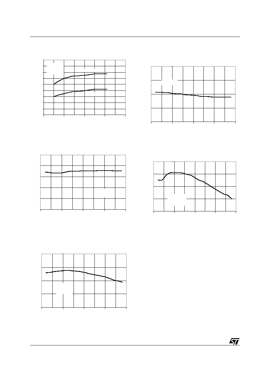
Figure 1. Line Regulation
Figure 2. Output Voltage vs. Junction
Temperature
Figure 3. Quiescent Current vs. Junction
Temperature
Figure 4. Shutdown Current vs.Junction
Temperature
Figure 5. Switching Frequency vs.Junction
Temperature
3.276
3.28
3.284
3.288
3.292
3.296
3.3
3.304
3.308
3.312
0
10
20
30
40
Vcc (V)
Tj = 125∞C
Tj = 25∞C
Vcc = 12V
Vo = 3.3V
Vo (V)
Tj (∞C)
Vcc=12V
1.2
1.21
1.22
1.23
1.24
1.25
-50
0
50
100
150
Vo (V)
Vcc = 12V
1.2
1.4
1.6
1.8
2
-50
0
50
100
150
Tj (∞C)
Iq (mA)
Vcc = 12V
DC = 0%
30
40
50
60
70
-50
0
50
100
150
Ishd (
µ
A)
Vcc = 12V
Tj (∞C)
220
230
240
250
260
-50
0
50
100
150
Tj (∞C)
Fsw (KHz)
Vcc = 12V
Vo = 3.3V

5/10
L5973D
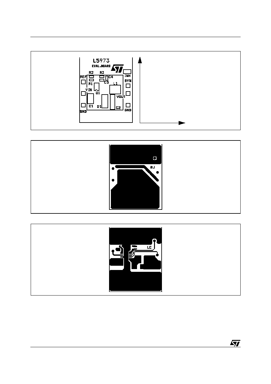
APPLICATION CIRCUIT
In figure 6 is shown the demo board application circuit, where the input supply voltage, V
cc
, can range from 4.4V
to 25V due to the rated voltage of the input capacitor and the output voltage is adjustable from 1.235V to V
cc
.
Figure 6. Demo board Application Circuit
Table 1. Component List
Reference
Part Number
Description
Manufacturer
C1
10
µ
F, 25V
TOKIN
C2
POSCAP 6TPB330M
330
µ
F, 6.3V
Sanyo
C3
C1206C221J5GAC
220pF, 5%, 50V
KEMET
C4
C1206C223K5RAC
22nF, 10%, 50V
KEMET
R1
5.6K, 1%, 0.1W 0603
Neohm
R2
3.3K, 1%, 0.1W 0603
Neohm
R3
4.7K, 1%, 0.1W 0603
Neohm
D1
STPS2L25U
2A, 25V
ST
L1
DO3316P-153
15
µ
H, 3A
COILCRAFT
D03IN1440
8
4
5
1
7
L5973D
C1
10
µ
F
25V
CERAMIC
C2
330
µ
F
6.3V
VOUT=3.3V
VIN = 4.4V to 25V
R1
5.6K
R2
3.3K
R3
4.7K
C4
22nF
C3
220pF
3
L1 15
µ
H
D1
STPS2L25U
COMP
VCC
OUT
FB
GND
INH
2
6
3.3V
SYNC.
VREF
L5973D
6/10
Figure 7. PCB layout (component side)
Figure 8. PCB layout (bottom side)
Figure 9. PCB layout (front side)
Below some graphs show the Tj versus output current in different conditions of the input and output voltage and
some efficiency measurements.
42mm
34mm

7/10
L5973D
Figure 10. Junction Temperature vs. Output
Current
Figure 11. Junction Temperature vs. Output
Current
Figure 12. Efficiency vs. Output Current
Figure 13. Efficiency vs. Output Current
20
30
40
50
60
70
80
90
100
110
120
0.2 0.4 0.6 0.8 1
1.2 1.4 1.6 1.8 2
2.2 2.4 2.6
Io(A)
Tj(∞C)
Vin=5V
Tamb=25∞C
Vo=2.5V
Vo=3.3V
Vo=1.8V
20
30
40
50
60
70
80
90
100
110
120
0.2 0.4 0.6 0.8
1
1.2 1.4 1.6 1.8
2
2.2 2.4 2.6
Io (A)
Tj (∞C)
Vin=12V
Tamb=25∞C
Vo=3.3V
Vo=2.5V
Vo=5V
67
69
71
73
75
77
79
81
83
85
87
89
91
93
95
0.1 0.3 0.5 0.7
0.9 1.1 1.3 1.5
1.7 1.9 2.1
2.3
Io (A)
E
ffi
c
i
e
n
c
y
(%
)
Vo=2.5V
Vo=3.3V
Vo=1.8V
Vin=5V
65
67
69
71
73
75
77
79
81
83
85
87
89
91
0.1 0.3 0.5 0.7 0.9 1.1 1.3 1.5 1.7
1.9 2.1 2.3
Io (A)
E
f
f
i
ci
en
cy (
%
)
Vo=2.5V
Vo=3.3V
Vo=5V
Vin=12V
L5973D
8/10
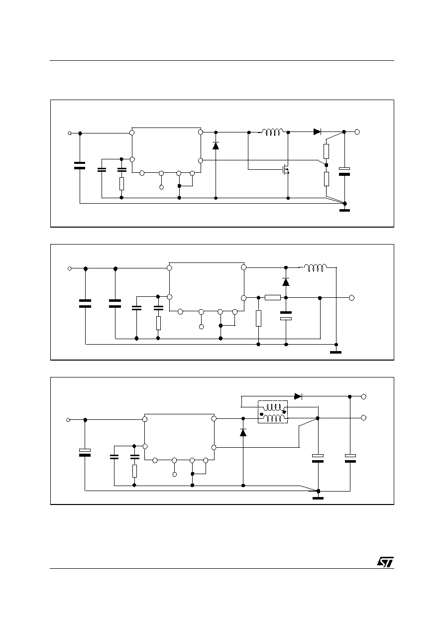
APPLICATION IDEAS
Figure 14. Positive Buck-Boost regulator
Figure 15. Buck-Boost regulator
Figure 16. Dual output voltage with auxiliary winding
VIN=5V
C1
10uF
10V
Ceramic
D1
STPS2L25U
Vcc
COMP
GND
OUT
FB
INH
SYNC
VREF
L5973D
1
3
7
5
6
4
8
2
R3
4.7k
L1
15uH
24k
2.7k
C3
22nF
3.3V
C4
100uF
16V
VOUT=12V/0.6A
C2
220pF
D2
STPS2L25U
M1
STN4NE03L
VIN=5V
C1
10uF
10V
Ceramic
D1
STPS2L25U
Vcc
COMP
GND
OUT
FB
INH
SYNC VREF
L5973D
1
3
7
5
6
4
8
2
R3
4.7k
L1
15uH
2.7k
24k
C4
22nF
3.3V
C5
100uF
16V
VOUT=-12V/0.6A
C3
220pF
C2
10uF
25V
Ceramic
VIN=12V
C1
10uF
25V
Ceramic
D1
STPS25L25U
VCC
COMP
GND
OUT
FB
INH
SYNC VREF
L5973D
1
3
7
5
6
4
8
2
R3
4.7k
C3
22nF
3.3V
VOUT=3.3V
0.5A
C2
220pF
VOUT1=5V
50mA
C5
47uF
10V
Lp=22uH
D2
1N4148
C4
100uF
10V
N1/N2=2
9/10
L5973D
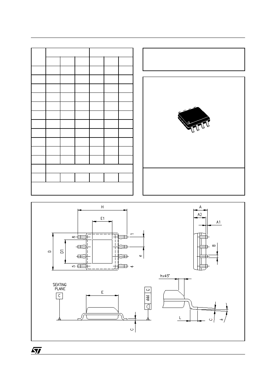
OUTLINE AND
MECHANICAL DATA
DIM.
mm
inch
MIN.
TYP.
MAX.
MIN.
TYP.
MAX.
A
1.350
1.750
0.531
0.069
0.100
0.250
0.004
0.010
1.100
1.650
0.043
0.065
0.330
0.510
0.013
0.020
0.190
0.250
0.07
0.010
4.800
5.000
0.189
0.197
3.800
4.000
0.150
0.157
1.270
0.05
5.800
6.200
0.228
0.244
0.250
0.500
0.010
0.020
0.400
1.270
0.016
0.05
k
0∞ (min), 8∞ (max)
ddd
0.100
0.010
(1) Dimension D does not include mold flash, protusions
or gate burrs shall not exeed 0.15mm (both side).
HSOP8
7195016
(Exposed Pad)
A1
A2
B
C
D
E
e
H
h
L
Exposed Pad:
D1 = 3.1mm
E1 = 2.41mm

Information furnished is believed to be accurate and reliable. However, STMicroelectronics assumes no responsibility for the consequences
of use of such information nor for any infringement of patents or other rights of third parties which may result from its use. No license is granted
by implication or otherwise under any patent or patent rights of STMicroelectronics. Specifications mentioned in this publication are subject
to change without notice. This publication supersedes and replaces all information previously supplied. STMicroelectronics products are not
authorized for use as critical components in life support devices or systems without express written approval of STMicroelectronics.
The ST logo is a registered trademark of STMicroelectronics.
All other names are the property of their respective owners
© 2003 STMicroelectronics - All rights reserved
STMicroelectronics GROUP OF COMPANIES
Australia - Belgium - Brazil - Canada - China - Czech Republic - Finland - France - Germany - Hong Kong - India - Israel - Italy - Japan -
Malaysia - Malta - Morocco - Singapore - Spain - Sweden - Switzerland - United Kingdom - United States
www.st.com
10/10
L5973D