 | –≠–ª–µ–∫—Ç—Ä–æ–Ω–Ω—ã–π –∫–æ–º–ø–æ–Ω–µ–Ω—Ç: L6000 | –°–∫–∞—á–∞—Ç—å:  PDF PDF  ZIP ZIP |

L6000
SINGLE CHIP READ & WRITE CHANNEL
ADVANCE DATA
SUPPORTS 9-32Mbit/s DATA RATE OPERA-
TION IN RLL [1,7] CONSTRAINT
- Data Rate is Programmable
SUPPORTS ZONED BIT RECORDING AP-
PLICATIONS
LOW POWER OPERATION (500mW TYPI-
CAL @ 5V @ 32Mbits/Sec
PROVIDES PROGRAMMABILITY THROUGH
SERIAL MICROPROCESSOR INTERFACE
AND INTERNAL REGISTERS
- Bi-directional access to internal registers of
pulse detector, filter, servo demodulator,
frequency synthesizer and data separator.
PROGRAMMABLE POWER DOWN MODES
Full power-down mode (5mW max.)
POWER SUPPLY RANGE 4.3 to 5.5V
DESCRIPTION
The L6000 is a 5V single chip read channel IC. It
contains all the functions needed to implement a
high performance read channel including the
pulse detector, programmable active filter, servo
demodulator, frequency sinthesizer, and data
separator, at data rates up to 32 Mbit/s. A single
external resistor sets the reference current for the
internal DAC which, in turn, fixes the data rate.
This device is programmed through a serial port
and banks of internal registers. It is fully compat-
ible with zoned bit recording applications. Exter-
nal components do not need to be changed when
switching between zones. The L6000 is manufac-
tured using an advanced BiCMOS technology.
This is advanced information on a new product now in development or undergoing evaluation. Details are subject to change without notice.
August 1993
43
42
41
40
39
23
24
25
26
27
DATA PATH
FI LT NORM OUT
FI LT NORM OUT
FI LT DIFF OUT
FI LT DIFF OUT
READ REF CLOC K
WRIT E CLOC K
MULT T P1
MULT T P2
GND I/O
DATA
TC
RES
SERVO
TC
RES
DAC
TP
OUT
GND
CORE
DIG
SERVO
GATE
PWRDN
MODE
VCC
CORE
DIG
SERIAL
DATA
I/O
SERIAL
CLOCK
+
SERIAL
ENABLE
M92L6000-01
54
55
56
57
58
18
19
20
21
22
VCC PULSE DET
FILT ER IN
FILT ER IN
PTAT R
AGC O UT
WRIT E DATA NR2 IN
READ NR2 O UTPUT
WRIT E DATA
VCC I/O
WRIT E GATE
38
37
36
35
34
11
12
13
14
15
HOLD
SRV
AGC
LATCH
CAP
A
LATCH
CAP
B
RESET
CAP
A/B
GND
DATA
SEP
REFERENCE
FIN
GND
FREO
SYN
FREQ
OUT
TP
VCC
FREQ
SYN
FREQ
SYN
FLT
33
16
DS
IREF
FREQ
SYN
FLT
59
17
AGC O UT
READ GATE
60
61
62
63
64
6
7
8
9
10
48
47
46
45
44
SERVO
BYP
SERVO
REF
V
POSITION
OUT
HOLD
CAP
A
HOLD
CAP
B
AGC
IN
AGC
IN
DATA
BYP
HOLD
DATA
AGC
GND
PULSE
DET
1
2
3
4
5
28
29
30
31
32
LEVEL
LEVEL REF V
CLOC K PATH
CLOC K PATH
DATA PATH
DATA SEP FLT
DATA SEP FLT
VCC DATA SEP
READ DATA I/O
ADDR MARK DET
49
50
51
52
53
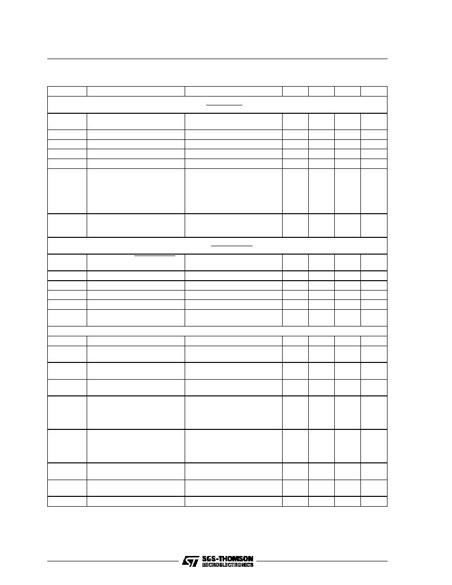
PIN CONNECTION (Top view)
ORDERING NUMBER: L6000
OPERATING TEMPERATURE: 0
∞
C to 70
∞
C
TQFP64
(10 x 10)
1/24

Figure 1a: Block Diagram (1 of 2)
L6000
2/24

Figure 1b: Block Diagram (2 of 2)
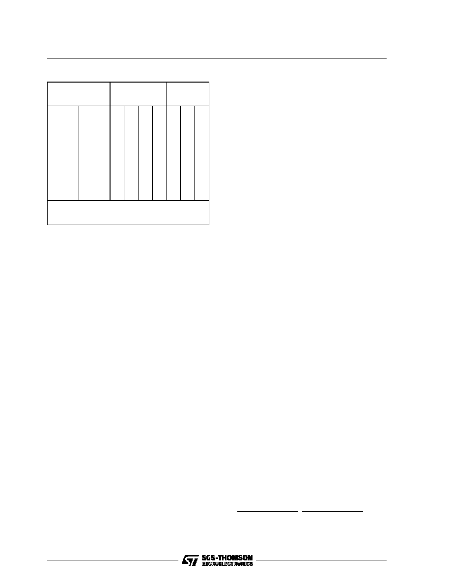
ABSOLUTE MAXIMUM RATINGS
Symbol
Parameter
Value
Unit
Vcc
Positive Supply Voltage
≠ 0.5 to 7
V
Voltage Applied to Logic Inputs
≠ 0.5 to Vccs + 0.5
V
Voltage Applied to All Other Pins
≠ 0.5 to Vccs +0.5
V
Tstg
Storage Temperature
≠ 65 to +150
o
C
Tj
Junction Temperature
130
o
C
L6000
3/24

PIN DESCRIPTION
Pin #
Symbol
Type
Description
POWER SUPPLY
30
Vcc DATA SEP
-
DATA SEPARATOR: PLL analog 5V supply.
14
Vcc FREQ. SYNTH
-
FREQUENCY SYNTHESIZER: PLL analog 5V supply.
7
Vcc CORE DIG
-
Internal ECL, CMOS logic digital supply.
19
Vcc I/O
TTL BUFFER I/O 5V SUPPLY.
59
Vcc PULSE DET
-
Pulse Detector/Servo Demodulator/Filter analog 5V supply.
34
GND DATA SEP
-
DATA SEPARATOR: PLL analog 5V ground.
12
GND FREQ SYN
-
FREQUENCY SYNTHESIZERl: PLL analog 5Vground.
40
GND CORE DIG
-
Internal ECL, CMOS logic digital ground.
23
GND I/O
-
TTL Buffer I/O digital ground.
5
GND PULSE DET
-
Pulse Detector/Servo Demodulator/Filter analog circuit ground.
INPUT
2, 1
AGC IN,
AGC IN
|
AGC AMPLIFIER INPUTS: Differential AGC amplifier input pins.
53, 54
DATA PATH,
DATA PATH
I
ANALOG INPUTS FOR DATA PATH: Differential analog inputs to data
comparators, full-wave rectifier, and servo demodulator.
51, 52
CLOCK PATH,
CLOCK PATH
I
ANALOG INPUTS FOR CLOCK PATH: Differential analog inputs to the clock
comparator.
6
PWRDN MODE
I
PWRDN MODE CONTROL: TTL compatible power control pin. Assertion shuts
down all circuitry, except the serial port. Deassertion and the appropriate bit set
in PD register shuts down the selected circuitry. Active low.
4
HOLD DATA AGC
I
HOLD DATA AGC CONTROL INPUT: TTL compatible power control pin.
Assertion disables the AGC charge pump and holds the input AGC amplifier
gain. Active low.
38
HOLD SRV AGC
I
HOLD DATA AGC CONTROL INPUT: TTL compatible control pin. Assertion
disables the SERVO charge pump. Active low.
47
SERVO REF V
I
SERVO REFERENCE .VOLTAGE INPUT: This voltage is set to half of the Vcc
PULSE DET voltage
37
LATCH CAP A
I
LATCH CONTROL INPUT: TTL compatible input. Switches channel A into
peak acquisition mode when low. Cap voltage doesn't change when high.
36
LATCH CAP B
I
LATCH CONTROL INPUT: TTL compatible input. Switches channel B into
peak acquisition mode when low. Cap voltage doesn't change when high.
35
RESET CAP A/B
I
RESET CONTROL INPUT: TTL compatible input. Enables the discharge of
channel A & B hold capacitors when asserted. Active low.
60, 61
FILTER IN,
FIL TER IN
I
FILTER SIGNAL INPUTS: Self biased differential input signals to active filter.
11
REFERENCE FIN
I
REFERENCE FREQUENCY INPUT: TTL input. Pin REFERENCE FIN has an
internal pull up resistor. In the test mode, when frequency synthesizer is
bypassed, the REFERENCE FIN frequency required is 3 times the data rate.
REFERENCE FIN may be driven by a direct coupled TTL signal.
22
WRT DATA NRZ
IN
I
WRITE DATA NRZ INPUT. TTL input. Connected to the READ NRZ OUTPUT
pin to form a bidirectional data port. Pin WRT DATA NRZ IN has an internal
pull up resistor.
17
READ GATE
I
READ GATE : See clocks and Modes.
26
WRITE CLOCK
I
WRITE CLOCK: TTL input Write mode clock. Must be synchronous with the
Write Data NRZ input. For short cable delays, WRITE CLOCK may be
connected directly to pin READ REF CLOCK. For long cable delays,WRITE
CLOCK should be connected to a READ REF CLOCK return line matched to
the NRZ data bus line delay.
18
WRITE GATE
I
WRITE GATE: TTL input. Enables the write mode. See Clocks and Modes.
39
SERVO GATE
I
SERVO GATE: TTL input. Enables the servo read mode. Active low.
L6000
4/24

PIN DESCRIPTION (continued)
Pin #
Symbol
Type
Description
OUTPUT
64, 63
AGC OUT,
AGC OUT
O
AGC AMPLIFIER OUTPUT: Differential AGC amplifier output pins.
29
READ DATA I/O
I/O
READ DATA I/O: Bi-directional TTL pin. Output is active in the servo mode or
when both READ GATE and WRITE GATE are deasserted. In test mode, this
is a TTL input used to drive the data separator. The TTL input is enabled by
setting RDI in the control register CB.
46
POSITION OUT
O
POSITION ERROR SIGNAL: A Position error signal of A minus B output which
is referenced to SERVO REF V.
56, 55
FILT NORM OUT,
FILT NORM OUT
O
FILTER DIFFERENTIAL NORMAL OUTPUTS: Low pass & boosted filter
output signals. Must be AC coupled to the next stage nominally DATA PATH.
58, 57
FILT DIFF OUT,
FILT DIFF OUT
O
FILTER DIFFERENTIAL DIFFERENTIADED OUTPUTS: Differentiated filter
outputs should be AC coupled to the next stage nominally CLOCK PATH.
28
ADDR MARK DET
O
ADDRESS MARK DETECT: Tristate output pin with TTL output levels. It is in
its high impedance state when WRITE GATE is asserted. When READ GATE
is asserted and the register bit is set for soft sector, an address mark search is
initiated in the soft sector operation. This output is latched low (true) when an
address mark has been detected. Deasserting pin READ GATE deasserts pin
ADDR MARK DET.
25
MULT TP1
O
MULTIPLEXED TEST POINT OUTPUT: An open emitter ECL output test point.
The test point output is enabled by Setting ED in the control registerCB. The
controlling signal is PD_TEST in the control register CA. When PD_TEST is low ,
the test point output is the delayed read data DRD. The posistive edges of this
signal indicate the data bit position. The positive edges of the DRD and VCOREF
outputs can be used to estimate window centering. The time jitter of DRD's
positive edge is an indication of media bit jitter. When PD_TEST is high the test
point out is the comparator of the pulse qualifier. The positive edge indicates that
the input signal has exceeded the positive threshold while a negative edge
indicates that the input signal has gone below the negative threshold. Two external
resistors are required to use this pin. They should be removed during normal
operation to reduce power dissipation.
21
READ NRZ
OUTPUT
O
NRZ OUTPUT DATA: Tristate ouput pin with TTL output levels. It is in its high
impedance state when READ GATE is deasserted. Read data output when
READ GATE is asserted.
27
READ REF CLOCK
0
READ REFERENCE CLOCK: TTL output. A multiplexed clock source used by
the controller, see Clocks and Modes. During a mode change, no glitches are
generated and no more than one lost clock pulse will occur. READ REF
CLOCK remains Fout/3 after READ GATE is asserted, until after synchronized
bits are detected.
24
MULT TP2
O
MULTIPLEXED TEST POINT OUTPUT: An open emitter ECL output test point.
This test point output is enabled by using the same control bit enabling the
MULT TP1 output. When the controlling signal, PD_TEST is desserted, the test
point output is the VCO reference input (VCOREF) to the phase detector. The
positive edges are phase locked to Delayed Read Data (DRD). The negative
edges of this open emitter output signal indicate the edges of the decode
window. When PD_TEST is high, the test point output represents the state of
the clock comparator in the pulse qualifier. The signal transitions indicate zero
crossing of the differentiated signal from the electronic filter. Two external
resistor are required to use this pin. They should be removed during normal
operation to reduce power dissipation.
20
WRITE DATA
O
WRITE DATA: TTL output. Encoded write data output. The data is
automatically resynchronized (independent of the delay between READ REF
CLOCK and WRITE CLOCK) to the reference clock FSout. Falling edge of the
WRITE DATA is the data edge.
13
FREQ OUT TP
O
REFERENCE FREQUENCY OUTPUT: An open emitter ECL output test point.
The frequency is the frequency synthesizer output frequency. This output is
enabled by control register CA. Two external resistors are required to use this
pin. They should be removed during normal operation to reduce power
dissipation.
L6000
5/24

PIN DESCRIPTION (continued)
Pin #
Symbol
Type
Description
ANALOG
50
LEVEL REF V
O
REFERENCE VOLTAGE: Reference voltage output for LEVEL. LEVEL REF V
is derived by referencing VRG (an internal signal) to Vcc PULSE DET.
62
EF IREF
I
REFERENCE RESISTOR INPUT: An external 1% resistor (RX) is connected
from this pin to ground to establish a precise reference current for the filter.
3
DATA BYP
≠
AGC INTEGRATING CAPACITOR: Connected between DATA BYP and Vcc
PULSE DET. This pin is used when data read mode.
48
SERVO BYP
≠
AGC INTEGRATING CAPACITOR FOR SERVO: Connected between SERVO
BYP and Vcc PULSE DET. This pin is used when in servo read mode
45
HOLD CAP A
≠
PEAK HOLDING CAPACITOR A: Tied from this pin to GND PULSE DET.
44
HOLD CAP B
≠
PEAK HOLDING CAPACITOR B: Tied from this pin to GND PULSE DET.
49
LEVEL
O
HYSTERESIS LEVEL: An NPN emitter output that provides a full-wave
rectified signal from LEVEL to LEVEL REF V to set the hysteresis threshold
time constant in conjunction with SERVO TC RES and DATA TC RES. This
level used in VTHRESHOLD DAC.
33
DS IREF
I
REFERENCE RESISTOR INPUT: An external 1% resistor (RR) is connected
to this pin to establish a precise internal reference current for the data
separator and Frequency Synthesizer.
42
SERVO TC RES
I
SERVO TIME CONSTANT RESISTOR INPUT: An external resistor is
connected from this pin to LEVEL to establish the hysteresis threshold time
constant when not in Servo mode.
15, 16
FREQ SYN FLT,
FREQ SYN FLT
≠
PLL FILTER: The two connection points for the frequency synthesizer PLL
differential filter components.
32, 31
DATA SEP FLT,
DATA SEP FLT
≠
PLL FILTER: THE Two connection points for the data separatorPLL differential
filter components.
41
DAC TP OUT
O
DAC OUTPUT: A test point for some of the on-chip DACs. The output of an
internal DAC is selected by the values of TDAC1 (MSB) and TDACO (LSB) in
the WS register. The selected DAc output and its corresponding select bits are
as follows: FC_DAC (00), VTH_DAC (0 1), WS_DAC (1 0), and WP_DAC (1
1). When not using the DAC TP OUT pin, the preferred setting is to select the
FC_DAC.
SERIAL PORT
10
SERIAL ENABLE
I
SERIAL DATA ENABLE: Active high input pin to enable the serial port CMOS
input levels.
8
SERIAL DATA I/O
I/O
SERIAL DATA: Input/Output pin for serial data; 8 instruction/address bits are
sent first followed by 8 data bits. CMOS Input/Output levels.
9
SERIAL CLOCK+
I
SERIAL DATA CLOCK: Positive edge triggered clock input for the serial data
CMOS input levels. The pin has an internal pull-up resistor.
L6000
6/24

SYSTEM DESCRIPTION
Pulse Detector Section
Fast attack/decay modes for rapid AGC recovery.
Dual rate charge pump for fast transient recovery.
Low Drift AGC hold circuitry supports programma-
ble gain, non-AGC operation. Temperature com-
pensated, exponential control AGC. Shorted input
switch for transient recovery, during Power down
& Write to read & Idle mode transitions. Wide
Bandwidth, high precision full-wave rectifier. Dual
mode pulse qualification circuitry allows either in-
dependent positive and negative threshold qualifi-
cation to suppress error propagation or hysteresis
comparison wich implements alternating polari-
ties. Differential qualifier comparator. TTL READ
DATA I/O signal
output available during servo
and idle modes. Timing for shorted inputs and
fast decay functions set internally. 0.5 ns max.
pulse pairing with sine wave input.
Embedded Servo Demodulator Section
Dual servo burst (A/B) capture with Position Error
Signal Output. Servo AGC mode which holds sum
of A and B bursts constant. Provision for on-chip
switching of the hysteresis threshold time con-
stant.
Programmable Filter Section
Programmable filter cutoff frequency (fc = 6 to 18
MHz). Programmable pulse slimming equalization
(0 to 9 dB Boost at the filter cutoff frequency).
Matched path timing normal and differential low-
pass outputs. Differential filter input and outputs
for noise rejection
±
10% cutoff frequency accu-
racy.
±
2% maximum group delay variation in the
passband maintained over the cutoff frequency
tuning range ( fc=6 to 18 MHz ). Total harmonic
distortion less than 1.5 %. No external filter com-
ponents required. Shorted input switch for tran-
sient recovery, during Power down & Write to
Read & Idle mode transitions.
Frequency Synthesizer and Data Separator
Section
1% frequency resolution. Data synchronizer and
1.7 RLL ENDEC. Fast acquisition phase lock loop
with zero phase restart both to data and synthe-
sizer. Fully integrated data separator. No external
delay lines or active devices required. No external
active PLL components required. Active window
centering symmetry control via serial port. Win-
dow shift control
±
30%. Includes delayed read
data and VCO clock monitor tests points. Pro-
grammable write precompensation. Hard and soft
sector operation.
THERMAL DATA
Symbol
Parameter
Value
Unit
Rth
j-amb
Thermal Resistance Junction-Ambient
100
∞
C/W
R
th j-case
Thermal Resistance Junction-Case
20
∞
C/W
RECOMMENDED OPERATING CONDITIONS
Vccn
Supply Voltage
4.3 to 5.5
V
T
amb
Operating Ambient temperature
0 to 70
∞
C
T
j
Junction Temperature
25 to 125
∞
C
L6000
7/24

ELECTRICAL CHARACTERISTICS: V
CCn
= 5V + 10% - 14%, T
amb
= 0 to 70
∞
C, Tj = 25 to 125
∞
C, un-
less otherwise specified.
Symbol
Parameter
Test Condition
Min.
Typ.
Max.
Unit
POWER SUPPLY CURRENT AND POWER DISSIPATION
Icc
Power Supply Current
Outputs and test point pins open;
Tamb = 27
∞
C, 32Mbits/sec
≠
100
120
mA
Pd
Power Dissipation
≠
500
660
mW
DIGITAL INPUTS AND OUTPUTS
V
IL
Low Level Input Voltage
≠ 0.3
0.8
V
V
IH
High Level Input Voltage
2.0
V
CC
I/O+0.3
V
I
IL
Low Level Input Current
V
IL
= 0.4V
≠
≠ 0.4
mA
I
IH
Low Level Input Current
V
IH
= 2.4V
≠
100
µ
A
V
OL
Low Level Output Voltage
I
OL
= 4.0mA
≠
0.5
V
V
OH
High Level Output Voltage
I
OH
= ≠400
µ
A
2.4
≠
V
CMOS INPUTS: SERIAL ENABLE, SERIAL DATA AND SERIAL CLOCK
V
IL
Low level Input Voltage
5V and 25
∞
C
≠
0.5
V
V
IH
High Level Input Voltage
4.5
≠
V
t
r
Rise Time
4.3V, 70
∞
C and C = 5pF
≠
5.0
ns
t
f
Fall Time
≠
4.5
ns
CMOS OUTPUTS: SERIAL DATA I/O
V
OL
Low Level Output Voltage
5V and 25
∞
C; I
OL
= 4.07mA
≠
0.5
V
V
OH
High Level Output Voltage
5V and 25
∞
C; I
OH
= +4.83mA
4.5
≠
V
t
r
Rise Time
4.3V, 70
∞
C and C = 15pF
≠
5.5
ns
t
f
Fall Time
≠
5.0
ns
TEST POINT OUTPUT LEVELS
V
IL
Test Point High Level Output
(MTP1, MTP2, FOUT)
261
to Vcc DATA SEP
402
to GND DATA SEP, Vcc
DATA SEP = 5V
Vcc
DATA
SEP-
1.02
≠
V
V
IH
Test Point Low Level Output
(MTP1, MTP2, FOUT)
261
to Vcc DATA SEP
402
to GND DATA SEP, Vcc
DATA SEP = 5V
≠
Vcc
DATA
SEP-
1.62
V
PULSE DETECTOR AND SERVO DEMODULATOR CHARACTERISTICS
Symbol
Parameter
Test Condition
Min.
Typ.
Max.
Unit
AGC Amplifier Section
The input signals are AC coupled to AGC IN and AGC IN. AGC OUT and AGC OUT are AC coupled to FILTER IN
and FILTER IN. FILT NORM OUT and FILT NORM OUT are AC coupled to DATA PATH and DATA PATH.
Integrating capacitor Ca = 1000pF is connected between DATA BYP and Vcc PULSE DET. Unless otherwise specified,
the output is measured differentially at AGC OUT and AGC OUT, Fin = 4MHz, and the filter boost at FB = 0dB.
Input range
Filter Boost at FC = 0dB
(bench test condition = 2.2 to
18MHz)
22
≠
240
mVpp
Input range
Filter Boost at FB = 9dB
Fin = FC = 18MHz
(bench test condition = 6 to
18MHz)
14
≠
100
mVpp
DATA PATH/
DATA PATH
Voltage
AGC IN-AGC IN = 0.1Vpp
0.945
1.05
1.155
Vpp
Voltage Variation
22mV < AGC IN = AGC IN <
240mV
≠8.0
≠
+8.0
%
Gain Range
1.9
≠
22
V/V
L6000
8/24

PULSE DETECTOR AND SERVO DEMODULATOR CHARACTERISTICS
Symbol
Parameter
Test Condition
Min.
Typ.
Max.
Unit
Gain Sensititivity with respect to
DATA BYP or SERVO BYPS
pin voltage changes
27
28
dB/V
AGC OUT/
AGC OUT
THD
AGCOUT - AGCOUT = 0.75Vpp
40
≠
≠
dB
Differential Input Impedance
WG = low
4.7
6
8.4
K
Single Ended Input Impedance
WG = low
WG = High or when IN Low - Z
mode
2.5
3.5
0.65
4.5
0.8
K
K
VOO
Output Offset Voltage
Filter not connected
≠ 200
≠
+200
mV
en
Input Noise Voltage
AGC OUT, Rs = 0
, gain = 22
≠
10
15
nV/
Hz
BW
Bandwidth
gain = 22
(1)
50
≠
≠
MHz
AGC OUT/
AGC OUT
Single ended output resistance
I
O
= 0
140
180
PSRR
Power Supply Rejection Ratio
gain = 22, Fin = 5MHz
45
dB
CMRR
Common Mode Rejection Ratio
40
≠
≠
dB
Gain Decay Time
AGC IN-AGC IN = 240mVpp to
120mVpp,
AGC OUT-AGC OUT = 0.9
Final Value
≠
≠
53
µ
s
Gain Attack Time
AGC IN-AGC IN = 120mVpp to
240mVpp,
AGC OUT-AGC OUT = 1.1
Final Value
≠
≠
2
µ
s
AGC Control Section
The input signal are AC coupled to DATA PATH and DATA PATH, C = 1000pF.
DATA PATH/
DATA PATH
Signal Input range
(bench test only)
≠
1
1.5
Vpp
Id
Discharge Current
2.8
4
5.2
µ
A
Idf
Fast Discharge
During Fast Decay mode
Current
20xld
≠30%
20xld
20xld
+30%
µ
A
Ich
Charge Pump Attack Current
DATA PATH-DATA PATH =
1.15Vpp
0.126
0.18
0.234
µ
A
Ichf
Charge Pump Fast Attack
Current
DATA PATH-DATA PATH =
1.45V
7xlch
≠30%
7xlch
7xlch
+30%
µ
A
DATA BYP Pin Leakage Current
WG = high
-0.1
+0.1
µ
A
LEVEL REF V Reference Voltage
Vcc
PULSE
DET-
2.47
≠
Vcc
PULSE
DET-
2.0
V
LEVEL REF V Output Drive
-0.75
≠
0.75
mA
Duration of shorted input and
Fast Decay modes
(*)
≠
1
≠
µ
s
Level Output Gain
DATA PATH-DATA PATH = 0.5
to 1Vpp
0.60
0.67
0.75
V/Vpp
Level Output Bandwidth
f
IN
= 11MHz
≠
≠
2
dB
(2)
Level Offset Voltage
Output - LEVEL REF V
(I
L
= 40
µ
A)
≠40
≠
+40
mV
(2)
(*) Guaranted by design.
(1) For correlation automatic test is performed at ≠3.8dB.
(2) Test limits under evaluation.
L6000
9/24
PULSE DETECTOR AND SERVO DEMODULATOR CHARACTERISTICS (continued)
Symbol
Parameter
Test Condition
Min.
Typ.
Max.
Unit
Data Comparator Section
(The input signals are AC coupled to DATA PATH and DATA PATH)
DATA PATH/
DATA PATH
Signal Range
≠
1
1.5
Vpp
Differential Input resistance
8
≠
14
K
Differential Input capacitance
≠
≠
5
pF
Comparator Offset Voltage
(*)
≠
≠
±
4
mV
Threshold Voltage Hysteresis
(*)
≠
20Kth
≠
%
Kth
Threshold Voltage Gain
0.3
( LEVEL-LEVEL REF V)
0.75, Kth = VTHDAC*0.651/127,
38 < VTHDAC < 125,
Vthresh = KTH*(LEVEL-LEVEL
REF V), also, %hyst =
VTHDAC*97.6%/127
Kth-9%
Kth
Kth+9%
V/V
Minimum Threshold Voltage
LEVEL-LEVEL REF V
0.1V,
Vthmin = VTHDAC*0.099/127
(*)
≠
Vthmin
≠
V
Clocking Section
(The input signals are AC coupled to CLOCK PATH and CLOCK PATH)
CLOCK PATH-CLOCK PATH
Signal Range
≠
≠
1.5
Vpp
Comparator Offset Voltage
(*)
≠
≠
±
4
mV
Differential Input Resistance
8
≠
14
K
Differential Input Capacitance
≠
≠
5
pF
Pulse Paring
Vs = 1Vpp, F = 4MHz
≠
≠
0.5
ns
Prpagation Delay to READ
DATA I/O
Vs = 20mVpp sq. wave
4
12
20
ns
Servo Section
SERVO REF V Voltage Range
2.15V
SERVO REF V
2.75V
2.15
2.50
2.75
V
SERVO REF V Input Bias
Current
≠1
0.2
1
µ
A
Voltage Gain, SERVO REF V
to POSITION OUT
|HOLD CAP A-HOLD CAP B|
0.4V
0.98
1.0
1.02
v/v
POSIT ION OUT Pin Offset
Voltage
HOLD CAP A-HOLD CAP B =
0V, SERVO REF V = 2.50V
≠
0
±
12
mV
POSITI ON OUT Pin High
HOLD CAP A-HOLD CAP B =
+1.8V
Vcc
PULSE
≠
Vcc
PULSE
V
Level Output Voltage
SERVO REF V = 2.50V,
Isource = 0.5mA
DET-
1.5
DET-
0.3
POSITI ON OUT Pin Low
HOLD CAP A-HOLD CAP B =
-1.8V
GND
PULSE
≠
GND
PULSE
V
Level Output Voltage
SERVO REF V = 2.50V Isink =
0.5mA
DET
+0.3
DET
+1.5
RO
POSITI ON OUT Pin Output
Resistance
VNG+1.5V
POSITION
OUT
VPG-1.5V
≠
≠
50
POSIT ION OUT GAIN
(POSITION OUT-SERVO REF
V)/Vpp
1.8
V/Vpp
(2)
HOLD CAP A/B Charge Current
Absolute Value
4
≠
≠
mA
(*) Guaranted by design.
(2) Test limits under evaluation.
L6000
10/24

PULSE DETECTOR AND SERVO DEMODULATOR CHARACTERISTICS (continued)
Symbol
Parameter
Test Condition
Min.
Typ.
Max.
Unit
Id
HOLD CAP A/B Disch. Current
Absolute value
0.8
1.5
2.2
mA
ILKG
HOLD CAP A/B Leakage Cur.
≠
≠
±
0.5
µ
A
ILKG
SERVO BYP Pin Leakage Cur.
HOLDS = Low
≠
≠
±
0.2
µ
A
K4
SERVO BYP Pin
Charge/Discharge Current
450
640
880
µ
A/Vpp
K5
Ibyps = K4
[K5 -
DATAPATH
App
≠
DATAPATH
Bpp
]
0.70
1.00
1.30
V/V
Maximum SERVO BYP Pin
Charge Current
190
300
490
µ
A
Tper
READ DATA I/O Output Pulse
Period
CL
15pF
50
≠
≠
ns
T1
READ DATA I/O Output Pulse
Low Time
RDIO
0.8V
9
23
33
ns
Th
READ DATA I/O Output Pulse
High Time
RDIO
0.8V
29
≠
≠
ns
Tf
READ DATA I/O Output Pulse
Fail Time
CL
15pF, 2.0V to 0.8V
≠
≠
5
ns
Tr
READ DATA I/O Output Pulse
Rise Time
CL
15pF, 0.8V to 2.0V
≠
≠
8
ns
PROGRAMMABLE FILTER CHARACTERISTICS
Symbol
Parameter
Test Condition
Min.
Typ.
Max.
Unit
Test Condition s: Vccn = 5V + 10% - 14%, T
amb
= 0 to 70
∞
C, T
j
= 25 to 125
∞
C, unless otherwise specified.
The input signals are AC coupled to FILTER and FIL TER IN. C
22nF.
FC
Filter Cutoff Frequency,
f at -3dB point
FC = 0.141732MHz *FCDAC,
42
FCDAC
127, FCDAC is
value of frequency DAC
6
≠
18
MHz
FCA
Filter fc Accuracy
FCDAC = 127
≠ 10
≠
+10
%
AN
FILT NORM OUT Differential Gain
f = 0.67FC, FBDAC = 0
1.6
2
2.4
V/V
AD
FILT DIFF OUT Differential Gain
0.9AN
≠
1.1AN
V/V
FB
Frequency Boost @ FC
FB (dB) = 20log [0.0273
(FBDAC)+1], 0
FBDAC
127
FBDAC = 127
≠
13
≠
dB
@6dB; FBDAC = 36
@13dB; FBDAC = 127
≠ 0.75
≠2.0
≠
+ 0.75
+2.0
dB
dB
TGDO
Group Delay Variation without
Boost
FC = 6MHz to 18MHz,
f = 0.2FC to FC FBDAC = 0
≠ 3
≠
+ 3
%
(2)
FC = 6MHz to 18MHz,
FBDAC = 0, f = FC to 1.75FC
≠ 4
≠
+ 4
%
(2)
TGDB
Group Delay Variation with
Maximum Boost
FC = 6 to 18MHz,
f = 0.2 FC to FC, FBDAC = 127
≠ 3
≠
+3
%
(2)
FC = 6MHz to 18MHz,
FBDAC = 127, f = FC to 1.75FC
≠ 4
≠
+4
%
(2)
VIF
Filter Differential Input Dynamic
Range
THD = 1% max, f = 0.67FC,
FBDAC = 0
0.5
≠
≠
Vpp
THD = 2% max, f = 0.67FC,
FBDAC = 0
0.75
≠
≠
Vpp
RIN
Filter Diff. Input resistance
5.0
≠
≠
K
RIZ
Filter Diff. Input Resistance with
Shorted Inputs
Low ≠ Z mode
100
300
500
CIN
Filter Diff. Input Capacitance
≠
≠
7
pF
(2) Test limits under evaluation.
L6000
11/24

PROGRAMMABLE FILTER CHARACTERISTICS(continued)
Symbol
Parameter
Test Condition
Min.
Typ.
Max.
Unit
EOUT
Output Noise Voltage
Differentiated Output
BW = 100MHz, Rs = 50
FC = 18MHz, DACS = 0
≠
2
7
mVrms
Output Noise Voltage Normal
Output
≠
1.2
5
mVrms
Output Noise Voltage
Differentiated Output
BW = 100MHz, Rs = 50
FC = 18MHz, DACS = 127
≠
4.6
7
mVrms
Output Noise Voltage Normal
Output
≠
2
5
mVrms
IO-
Filter Output Sink Current
0.5
≠
≠
mA
IO+
Filter Output Source Current
2.0
≠
≠
mA
RO
Filter Output resistance Single
Ended
≠
≠
200
Note: FBDAC is value of boost DAC (i.e., no boost)
Filter Control Characteristics (RX = 12K
)
VRX
Reference Current Set Output
Voltage
T
amb
= 27
∞
C
(**)
≠
1.5
≠
V
FREQUENCY SYNTHESIZER CHARACTERISTICS (RR = 39K
)
FIN
Input Frequency
8
20
MHz
FOUT
Output Frequency
≠
96
MHz
JFO
FOUT jitter
TO = 1/FO; Fout = 30MHz
≠
±
400
ps(pk)
M Divide Number
80
255
≠
N Divide Number
25
127
≠
TVCO
VCO Center Frequency Period
TO = (9.65 + 0.843
x
DR)
-1
FLTR1-FLTR1 = 0 (***)
0.9TO
1.1TO
ns
VCO Frequency Dynamic
Range
≠1.5
FLTR1-FLTR1
+1.5,
Fout = 54.0MHz (***)
25
±
45
%
KVCO
VCO Control Gain
= 2
/TVCO
≠1.5
FLTR1-FLTR1
+1.5
0.14
o
0.26
o
rad/(V-s)
KD
Phase Detector Gain
KD = 0.7 + 0.43
x
DR (***)
0.83KD
1.17KD
µ
A/rad
KVCO x KD Product Accuracy
≠ 28
+ 28
%
Reference Clock Characteristics:
Reference Clock Low Time
20
≠
ns
Reference Clock High Time
20
≠
ns
DATA SEPARATOR DYNAMIC CHARACTERISTICS AND TIMING (Unless otherwise specified, rec-
ommended operating conditions apply.)
Real Mode
TRRC
Read Clock Rise Time
0.8V to 2.0V, CL
15pF
≠
8
ns
TFRC
Read Clock Fall time
2.0V to 0.8V, CL
15pF
≠
5
ns
RRC Duty Cycle
DR = 32Mbit/s
43
57
%
TNS, TNH
NRZ(out) Set Up and Hold Time
DR
20Mbit/s (**)
15.5
≠
ns
DR > 20Mbit/s (**)
13
≠
ns
TPNRZ
NRZ (out) Propagation Delay
(**)
≠
±
15
ns
(**) Bench test only.
(***) Preliminary data.
L6000
12/24

DATA SEPARATOR DYNAMIC CHARACTERISTICS AND TIMING (Continued)
Symbol
Parameter
Test Condition
Min.
Typ.
Max.
Unit
TAS, TAH
AMD Set Up and Hold Time
(**)
13
≠
ns
TPAMD
AMD Propagation Delay
(**)
≠
±
15
ns
TD
1/3 Cell Delay
TD = 1/FSOUT,RR = 39K
(***)
0.8TD
1.2TD
ns
Write Mode
TWD
Write Data Pulse Width
1.5V
2TFout/3
2TFout/3
ns
CL
15pF
≠ 5
+ 5
TRWD
Write Data Rise Time
0.8V to 2.0V, CL
15pF
≠
9
ns
TFWD
Write Data Fall Time
2.0V to 0.8V, CL
15pF
≠
5
ns
TRWC
Write Data Clock Rise Time
0.8V to 2.0V, CL
15pF
≠
10
ns
TFWC
Write Data Clock Fall Time
2.0V to 0.8V, CL
15pF
≠
8
ns
TSNRZ
NRZ Set Up Time
5
≠
ns
THNRZ
NRZ Hold Time
5
≠
ns
TPC
Precompensation Time Shift
Magnitude Accuracy
TPCO = 0.04TREF
TPC(max) = 0.28TREF
TPC = nTPCO
n =0
1
n
7
≠ 0.5
n(0.8TPCO)
≠ 0.5
+ 0.5
n(1.2TPCO)
+0.5
ns
ns
Data Synchronization
TVCO
VCO Center Frequency Period
FLTR2-FLTR2 = 0
TO = (8.95 + 0.786 x DR)
-1
,
RR = 39k
(***)
0.9TO
1.1TO
ns
VCO Frequency Dynamic range
≠1.5
FLTR-FLTR2
+1.5 (***)
±
25
±
45
%
KVCO
VCO Control Gain
o =
2
T
VCO
0.14Wo
0.26Wo rad/(Vxs)
≠1.5
FLTR-FLTR2
+1.5
KD
Phase Detector Gain
Read: KD = 0.7 + 0.43
x
DR,
PLL REF = RD 3T Pattern, Non-
Read: KD = 0.7 + 0.43
x
DR,
PLLREF = Fout / 2 (***)
0.83KD
1.17KD
A/rad
KVCO x KD Product Accuracy
≠ 28
+ 28
%
VCO Phase Restart Error
≠
4
ns
Decode Window Cent. Accuracy
≠
±
1.5
ns
Decode Window Width
2TORC/3
- 1.5
≠
ns
SERIAL PORT TIMING
Symbol
Parameter
Test Condition
Min.
Typ.
Max.
Unit
Tc
SERIAL CLOCK+ Data Clock Period
100
≠
ns
Tck1
SERIAL CLOCK+ Low Time
40
≠
ns
TcKh
SERIAL CLOCK+ High Time
40
≠
ns
Tsens
Enable to Clock Delay Time
35
≠
ns
Tsenh
Clock to Disable Delay Time
Delay from SERIAL
CLOCK+ falling edge
100
≠
ns
Tds
Data Setup Time
15
≠
ns
Tdh
Data Hold Time
15
≠
ns
Tdskewl
Clock to Valid Data Delay Time
Delay from SERIAL
CLOCK+ falling edge
≠
27
ns
Tdskewe
End of Valid Data to Clock
≠
0
ns
Tsendl
Time to Tri-stated SERIAL DATA I/O
Delay from falling edge
of SERIAL ENABLE
≠
50
ns
Tturnd
SERIAL DATA I/O Turnaround Time
70
≠
ns
Tsl
SERIAL ENABLE Low Time
200
≠
ns
(**) Bench test only. (***) Preliminary data.
L6000
13/24

MODE CONTROL
PWRDN Mode
Register bits
DESCRIPTION
WRITE
GATE
READ
GATE
SERVO
GATE
PWRDN
MODE
PD
SD
FLT
DS
FS
X
X
X
O
X
X
X
X
X
FULL POWER DOWN MODE : Only the serial interface
remains operational. Switching from this mode to either
Servo, Read or Idle modes initiates certain Read Channel
states. Switching direct to Write modes is an illegal sequence.
See Circuit Opertion.
0
1
1
1
0
0
0
0
0
READ MODE : The entire FRONT END is turned on, the
READ DATA I/O pin is inactive, and the AGC amplifier is
active, with unshorted inputs ( low-impedance mode off ) and
in tracking mode. The HOLD DATA AGC input is enabled.
The Data Separator section initiates its Address Mark search
on the assertion of READ GATE. It then starts its phase lock
up sequence aft er Address Mark detection occurs. After
3
3T following the Address Mark Detection the DS PLL
is switched from Fout/2 to DRD and the look-in sequence is
initiated. After 19
3T RRC switche from Fout/3 to DATA
SYNCHRONIZER Vco/3 and NRZOUT is enabled. After.
Read mode is maintained until the deassertion of READ
GATE.
1
0
1
1
0
0
0
0
0
WRITE MODE : The FRONT END is inactive. The assertion
of WRITE GATE causes the pin WRT DATA NRZ IN to
become an active input, and the pins READ NRZ OUTPUT
and ADDR MARK DET are floated. The inputs of both the
Active filter and AGC amplifier are shorted ( i.e. the low-
impedance state entered ). The PLL is locked to the
Frequency Synthesizer divided by 30. n WRITE GATE
assertion, two address marks ( each 7 0's, 1, 7 0's, 1, 11 0's,
1, 11 0's ) are generated and than the preamble of three 3T
groups. WRT DATA NRZ IN must be zero until these patterns
have been output from WRITE DATA. Write Mode is ended
when Write Gate is deasserted. This starts the AGC Amplifier
fast attack/decay currents acquisition, as well as unshorting
the filter and AGC Amplifier inputs.
0
0
1
1
0
0
0
0
0
IDLE MODE : Allthe front end circuitry is active and operating.
The Data Separator VCO is phase locked to Fout. The READ
REF CLOCK outputs is the Frequency Synthesizer divided by
3. The pin READ NRZ OUTPUT is floated, ADDR MARK DET
is high, READ DATA I/O is an active output of the pulses
detected and HOLD DATA AGC is enabled. The inputs to the
AGC Amplifier and filter are unshorted.
0
X
0
1
0
0
0
0
0
SERVO MODE 1 : The Pulse Detector and Servo
Demodulator circuitry is operating, and the HOLD DATA AGC
input is disabled. The Data Separator is on and it is phase
locked to the Frequency Sinthesizer which is also on. The pin
READ DATA I/O is an active output.
0
X
0
1
0
0
0
1
1
SERVO MODE 2 : This mode has both the Frequency
Synthesizer and Data Separator major blocks powered down,
otherwise it is the same as SERVO MODE 1 . This mode is
intended to reduce power dissipation when the systhem is
just track following. Since only the Pulse Detector and Active
Filter are powered on, this is also known as FRONT END
TEST MODE.
L6000
14/24

CIRCUIT OPERATION
General
The L6000 is a state of the art integrated read
channel. The major functional blocks are :
1) Pulse Detector and Servo Demodulator, with
dual servo burst measurement channels and
2 different qualification schemes for data.
2) Tunable Active equiripple filter with tunable
Pulse slimming Boost and Active Differentia-
tor.
3) (1, 7) RLL Combined Data Separator and
ENDEC with active window
centering and
margin shifting from external commands.
4) A (M+1) divide by (N+1) Frequency synthe-
sizer, using an external reference, and with 7
bits of DAC control accuracy.
5) A high speed serial interface controlling most
functions and adjustement.
The L6000 is designed to be used with data rates
as high as 32 Mbits/sec. Selection of a different
recording density is done by setting new divisors
in the Frequency Synthesizer via serial registers.
Power Management
The serial interface should load all appropriate
control registers as soon as Power on Reset
clears in the system. This prevents spurious con-
ditions in all the affected blocks. After the regis-
ters are written, then the appropriate Power down
modes can be used. The power management of
the L6000 is under the control of the PWRDN
MODE pin and the Power Down Control Register
(R02). The following table defines the power
down modes and register bits controlling them:
Bit
Symbol
Function
0
1
2
3
4
5-7
PD
SD
FLTR
DS
FS
Pulse Detector Power Down
Servo Demodulator Power Down
Filter Power down
Data Separator Power Down
Frequency Synthesizer Power Down
Bits 5-7 are Hard-Coded to 111.
When the PWRDN MODE pin is asserted it pow-
ers down ALL functions with the exception of the
serial port, which remains active in ALL power
down modes. When the PWRDN MODE pin is
deasserted, each individual major function block
can be powered on or OFF separately from the
serial port PD register. This feature is useful for
sophisticated power saving state machines in
systems. Toggling the bit in the register is the
only necessary condition to turn on or OFF a ma-
jor block; PWRDN MODE does not have to be cy-
cled for each separate register load.
Serial Interface
The serial interface consists of the 3 signals SE-
RIAL ENABLE, SERIAL CLOCK and SERIAL
DATA I/O. The first two signals are inputs which
are always powered on and active. SERIAL
DATA I/O is a bidirectional pin which becomes an
ouput on a register read. A value can be put into
the L6000 (register WRITE) or a value can be in-
terrogated from the L6000 (register READ). The
bottom half of the diagram is a register READ
where a value is interrogated from the L6000. To
do either operation, SERIAL DATA ENABLE is
MODE CONTROL(continued)
PWRDN Mode
Register bits
DESCRIPTION
WRITE
GATE
READ
GATE
SERVO
GATE
PWRDN
MODE
PD
SD
FLT
DS
FS
X
X
X
1
1
1
0
1
1
TEST FILTER MODE : All major blocks except the Active
Filter with Boost and Differentiator are powered down via
Register ( R02 ).
0
1
1
1
1
1
1
0
0
TEST DATA SEPARATOR READ MODE : Only the Data
Separator and Frequency Synthesizer are on, and the pin
READ DATA I/O is a test input.
1
0
1
1
1
1
1
0
0
TEST DATA SEPARATOR WRITE MODE : Only the Data
Separator Write circuitry and the Frequency Synthesizer are
on, for testing this specific circuitry.
X
X
X
1
1
1
1
0
0
TEST FREQUENCY SYNTHESIZER MODE: The front end is
powered down. The Frequency Synthesizer is powered on for
testing.
L6000
15/24

asserted, then the SERIAL CLOCK+ is driven
with the positive edge latching the state of SE-
RIAL DATA. The actual data is latched into each
register in the L6000 when SERIAL ENABLE is
disasserted, so this signal MUST be driven low
after EACH register write; failure to deassert SE-
RIAL ENABLE before a 17th SERIAL CLOCK+
will erase ( invalidate ) the previous 16 clock cy-
cles. This also precludes SERIAL CLOCK+ from
being a free running clock in the system. The
The internal register map for the serial port is shown below:
Address Bits
Blk Diagr.
Address
Symbol
Function
LSB
MSB
0
0
1
1
0
0
0
0
0
0
1
1
0
1
1
1
1
1
1
1
1
1
0
0
0
0
2
0
0
0
0
0
0
1
1
1
1
1
1
3
0
0
1
1
0
1
0
1
0
0
1
1
4
0
0
0
0
1
1
0
0
0
0
0
0
5
0
0
0
0
0
0
0
0
0
0
0
0
6
0
0
0
0
0
0
0
0
0
0
0
0
R02
R03
R0B
R0A
R12
R1A
R06
R0E
R04
R05
R0D
R0C
PD
FCutoff
FBoost
DVTH
SVTH
CA
PSNN
PSMM
VCO CENT
WIN SHIFT
WRT PREC
CB
Power Down Mode Control
DACF-Filter cutoff Frequency Control
DACS-Filter Boost Control
Pulse Detector Voltage Threshold Control (Data Read Mode)
Pulse Detector Voltage Threshold Control (Servo Read Mode)
Control A (Pulse Detector, Filter, frequency synthesizer Control)
Counter Value (frequency synthesizer)
Counter Value (frequency synthesizer)
VCO Center Frequency
Window Shift Magnitude,Direction
Write Precomp magnitude
Control B (Data Separator, Endec Control)
The bit map of each register (except CA, CB & PD) is as follows:
FCutoff register
FBoost register
DVTH register
SVTH register
PSN register
PSM register
VCO CENT register
WIN SHIFT register
WRT PREC register
X
X
DEDC
SEDC
X
M7
FSC
TDAC1
X
FC6
FB6
VD6
VS6
N6
M6
DR6
TDAC0
X
FC5
FB5
VD5
VS5
N5
M5
DR5
WSE
X
FC4
FB4
VD4
VS4
N4
M4
DR4
WSD
X
FC3
FB3
VD3
VS3
N3
M3
DR3
WS3
WP3
FC2
FB2
VD2
VS2
N2
M2
DR2
WS2
WP2
FC1
FB1
VD1
VS1
N1
M1
DR1
WS1
WP1
FC0
FB0
VD0
VS0
N0
M0
DR0
WS0
WP0
where:
X = Unused bit or don't care bit
DEDC = Enable dual comparator qualifier in Data read mode.
SEDC = Enable dual comparator qualifier in Servo read mode.
FSC = The frequency synthesizer back comparator state
TDAC1 = DAC Testing control bit #1
TDAC0 = DAC Testing control bit #0
Control register CA:
Control register CB:
Bit
Symbol
Function
Bit
Symbol
Function
0
EPDT
Enable Phase Detector (frequency
synthesizer)
0
DW
Direct Write (Bypass Endec)
1
UT
Pump Up (FLTR1 sources current,
FLTR1 sinks current) Test mode
1
GS
Enable Phase Detector Gain
Switching
2
DT
Pump Down (FLTR1 sinks current,
FLTR1 sources current) Test Mode
2
READ DATA I/O Pin Input Control
3
ET
Enable frequency synthesizer Circuit
Function
3
EPDD
Enable Phase Detector (Data
Separator)
4
BYPT
Bypass frequency synthesizer Circuit
Function
4
UD
Pump Up (FLTR2 sources current,
FLTR2 sinks current) Test mode
5
PD
TEST Enable Pulse Detector Test
Points, COUT and DOUT
5
DD
Pump Down (FLTR sinks current,
FLTR2 sources current) Test mode
6
FDCT
Force AGC Charge Pump into Fast
Decay Mode
6
ED
Enable Data Separator Test Point
Outputs
7
Unused
7
SOFT
Select Soft or Hard Sector Operation
L6000
16/24

WRITE operation format is the following. The first
bit is LOW, meaning write, followed by the 7bit
register address, LSB first. The last 8 bits then
are the data to be written to the register, also LSB
first. During this to entire operation, SERIAL
DATA I/O is an active input. The READ operation
format is the following. The first bit now is HIGH,
meaning read, and that is followed by the 7bit
register address, LSB first. Upon receipt of the
last bit of address, the pin SERIAL DATA I/O
turns and becomes an active output, and outputs
the 8 bits stored in the addressed register, LSB
first on the following 8 SERIAL CLOCK+s.
Pulse Detector and Servo Demodulator
The purpose of the Pulse Detector is to qualify
and detect the position of flux transitions written
on the disk. The first stage of the Pulse Detector
is the AGC amplifier. It is a wideband, differential
amplifier which characteristic (Gain vs. Voltage) is
positive slope and linear in DB and thermal com-
pensated. The amplifier inputs have a low-imped-
ance state where the inputs are shorted by a FET
switch during modes where transients are likely to
occur. The amplifier gain is controlled by 2 ca-
pacitors connected to to the DATA BYP and
SERVO BYP pins. The capacitor which controls
the gain is selected by the SERVO GATE signal,
asserted meaning Servo.
In modes where the
AGC is powered on, the selected capacitor will be
charged from a dual rate charge pump. When the
individual signals HOLD DATA AGC and HOLD
SERVO AGC are asserted, the respective capaci-
tors are disconnected from the charge pumps, but
they remain in control of the AGC gain. If a fixed
gain is desired, a voltage divider can be con-
nected to either DATA BYP or SERVO BYP pin.
In order to minimize the time required to restore
the correct AGC output amplitude, the input
switching to unshorted inputs and the AGC at-
tack/delay currents are under timed, state control.
The time to restore the inputs and AGC to normal
operation is set to 1 usec. However, the AGC at-
tack is controlled by amplitude and may take
longer to settle. The nominal AGC attack (dis-
charge) current is set to 0.18 mA but is increased
to 1.3 mA when the AGC amplitude exceedes
1.25 times its set point. The nominal AGC decay
current is increased from 0.004 mA to 0.080 mA
in the recovery fast/decay mode. The high decay
current of 80uA is only on for the second micro-
second after the mode switch initiates the AGC
reacquisition. Note that the fast Decay current is
available in the recovery mode, while any ampli-
tude transient over the threshold will activate the
fast Attack current.
The modes where the inputs go from shorted to
unshorted are :
1) From Full Power Down either Servo mode
(SERVO GATE active)
2) From Full Power Down to Idle mode.
3) From Full Power Down to Read mode.
4) From Write to Read mode.
5) From Write to Idle mode.
The modes where the inputs go from unshorted
to shorted are : 1) From Read to Write mode. 2)
From any mode to Full Power Down mode.
The modes where the fast attack and decay cur-
rents become active are :
1) From Full Power Down to Idle mode.
2) From Full Power Down to Read mode.
3) From Write to Read mode.
Nominally the AGC amplifier outputs will be AC
coupled to the Active Filter outputs and then the
Active Filter outputs, both Normal and Differential
will be AC coupled back to the Pulse Detector
block.
Pulse Detector
This block has 4 inputs, 2 fully differential pairs.
The CLOCK PATH inputs are a zero crossing de-
tector, zero crossing assumed to occur at the am-
plitude peaks of the pulses. This input pairs shall
be connected to the Active Filter differentiator.
The DATA PATH inputs are amplitude ( threshold
) qualifiers and are to be connected to the Active
Filter normal outputs. Call factory for schematic
for the recommended connection in the system.
Dual threshold comparators are available in the
Pulse Detector. If the DEDC bit is set in the
DataVth register ( ROA ), then separate compari-
sons are done on negative and positive peaks. If
the bit is reset, then the polarity of the next pulse
to be qualified must be opposite of the last. This
check can lead to a 2 bit missing error for just 1
pulse under threshold. The threshold used for
comparison is set in the two threshold register
DataVth and ServoVth. These register feed the
threshold DAC (VTHDAC) which developes the
actual floating hysteresis level and thresholds
from the input LEVEL (a bufferred signal rectified
from the filter normal outputs. The hysteresis is
always a percentage, of 0.7 the peak to peak
swing at DATA PATH inputs, and is accurate from
10 to 80 % with a 1 % accuracy. The floating hys-
teresis generator also has a time constant which
is developed from the components connected to
SERVO TC RES, DATA TC RES, LEVEL, and
LEVEL REF V. This time constant is, in effect, a
time domain filter implemented in the qualifier
channel that has the purpose to realize an enve-
lope detector on the rectified signal feeding the
DATA PATH inputs. The two constant is changed
depending on SERVO GATE state.. Recom-
mended values for Rext on SERVO TC RES and
DATA TC RES is TBD ; for Cext on LEVEL and
LEVEL REF V it is TBD. The output of the Pulse
Detector block is READ DATA I/O, and this pin is
active ONLY in the Idle and Servo modes. It is an
approximately 24 nsec negative going TTL com-
L6000
17/24

patible data pulse. The PD- Test bit of the register
CA controls this output being active. NORMAL
operation is for this bit to be reset , but for testing
the Data Separator as an input, it should be set.
Servo Demodulator
When in Servo mode all circuitry not needed to
acquire embedded servo position information is
deactivated, the AGC loop is switched to the
servo BYP capacitor, the READ DATA I/O output
is activated, the SERVO TC RES Servo time con-
stant setting resistor is connected to LEVEL REF
V, and the hysteresis threshold level is set to the
Servo threshold.
Three servo control inputs,
LATCH CAP A, LATCH CAP B, and RESET CAP
A/B
control the servo peak sample and hold
functions. When HOLD SERVO AGC is deas-
serted, the servo charge pump drives the SERVO
BYP hold capacitor. The current magnitude and
direction is determined by the formula :
Ibyp2 = gm1*( Vset-Va ( DIN ) pp-Vb ( DIN ) pp )
where : gm1 = 640 uA/Vpp
Vset = 1.0Vpp
Va/b( DIN ) pp = peak to peak A or B servo pat-
tern signal voltages across DATA PATH and
DATA PATH.
When SERVO GATE is deasserted, there is an
automatic 1 usec break before make switch in an
action before the capacitor on the DATA BYP pin
is reconnected to the AGC gain control.
The POSITION OUT pin outputs a voltage equal
to the difference beetwen HOLD CAP A and
HOLD CAP B referenced to SERVO REF V.
The DATA BYP and SERVO BYP capacitor volt-
ages will be held constant (subject to leakage cur-
rent) during sleep mode, when the respective
HOLD DATA AGC and HOLD SRV AGC signals
are low, and when they are not being used to
control the AGC loop.
Test bits and modes
The FDCT bit in the Control A register forces the
Charge pump into the fast decay (or 0.08 mA cur-
rent) mode. This bit should be set during power
up in a normal system. The PD_Test bit stands
for Pulse Detector Test and should be reset, so
that MULT TP1 outputs Delayed Read Data
(DRD), and MULT TP2 outputs the Data Separa-
tor VCO (divided by two).
Programmable Active Filter
The outputs of the AGC Amplifier of the Pulse De-
tector block are normally AC coupled to inputs of
the Active Filter. The low-pass portion of the ac-
tive filter is to bandlimit noise. The FCutoff regis-
ter is used to set the cutoff frequency of this por-
tion. The filter type is a 7 pole 0.05 degree
equiripple linear phase error low-pass. Shaping
response may also be introduced, via the boost
equalization available. This is done to account for
deficiencies in the recording process. The FBoost
register sets the amount and polarity of boosting
the cutoff
frequency
in the Active Filter. The
amount set is contained in the FB register. The
boost is accomplished by a two pole high-pass
feed forward section in parallel with the low-pass
filter. A differentiator is also part of the Active Fil-
ter major block to turn the recovered peaks into
zero crossing. The differentiator is a single pole,
single zero active type. The Active Filter block has
2 outputs. One set is the differential outputs from
the low-pass/equalization portion. The other set is
the differential outputs of differentiator portion.
Both sets of the outputs have matched delays to
maintain timing integrity when re-entering the
Pulse Detector major block. The current reference
for the FC and FB DAC is developed off of the EF
IREF input. The recommended value of the resis-
tor at EF IREF is : 12 Kohm
±
1% .
The normalized low-pass transfer function is :
(i.e.
c
= 2
fc = 1) are: (see Fig. 2 for reference)
Vnorm
Vi
= (
1
-
Ks
2
+
0.75928
)
D
(
s
)
AN
The normalized differentiator transfer function is :
Vdiff
Vi
= (
1
-
Ks
2
+
0.75928
)
s
1.16099
D
(
s
)
AD
where D(s) = (1 + s + 1.27936 + s
2
0.75928)
(1 + s 0.52247 + s
2
0.33882)
(1 + s 0.21323 + s
2
0.1862)
(1 + s 1.16099)
AN and AD are adjusted for a gain of 2 at fs =
(2/3)FC.
Frequency Synthesizer
The Frequency Synthesizer block is used to de-
velop source recording frequencies for writing
data in the system. It is Phase Lock Loop based
circuit with divide counters set by registers loaded
from the serial interface. The frequency gener-
ated, Fout, is 3 times the HOST data rate in
Mbits/sec, and is 2 times the CODE data rate of
pulses written on the disks. The resolution of the
frequency is 1%. The filter to the PLL is external,
and fully differential on the pins FREQ SYN FLT
and FREQ SYN FLT. A second order filter is rec-
ommended. The Fout frequency is used in Read,
Write and Idle modes as the reference for the
Data Separator PLL. If the ET bit of Control A reg-
ister is set in these modes the FRE OUT TP pin
will output the Synthesizer clock Fout. Setting this
bit in Read mode is not recommended in order to
reduce jitter and decrease power dissipation. To
set the frequency, the input REFERENCE FIN is
fed to the divide by N+1 counter, and this counter
output is the reference input of the Frequency
L6000
18/24

Synthesizer phase comparator. The Frequency
Synthesizer VCO is fed to divide by M+1 counter,
and the counter output is the other phase compa-
rator input.
This develops the frequency:
Fout
= (
M
+
1
)
(
N
+
1
)
FREF
Note : For the new value in the M and N registers to be transferred
to their respective counters, the VCO Center Frequency DAC register
must be loaded with its value. This means the normal order of register
writes to change the Frequency Synthesizer output frequency would
be:
1) Write M and/or N register with its ( their ) new value ( s ).
2) Write the VCO Center Frequency register with its new value.
The RREF is choosen to set the frequency range
of both the FDSVCO and the DSVCO.
CLOCKS AND MODES
WRITE
GATE
READ
GATE
VCO
REF
RRC
DECCLK ENCCLK
MODE
O
O
1
0
1
0
Fout/2
DRD
Fout/2
Fout/3
VCO/3
Fout/3
Fout/2
VCO/2
Fout/2
Fout/2
Fout/2
Fout/2
IDLE
READ
WRITE
Notes: 1 Until the VCO locks to the new source, the VCO/2 entries
will be FREQ OUT TP/2.
2: Until the VCO locks to the new source, the VCO/3 entries will be
FREQ OUT TP/3
3: WRI TE GATE = READ GATE = 1 is undefined and illegal
Data Separator
The data separator circuit is a complete 1.7 RLL
ENDEC data recovery circuit. In the read mode,
the circuit performs data synchronization, sync
field search and detect, address mark detect,
Read-back clock generation and data decoding.
In the write mode, the circuit converts NRZ data
into the ( 1.7 ) RLL format described in the Table
1, performs write precompensation, generates the
preamble field and inserts address marks as re-
quested.
The data rate used for recovery is determined by
the VCO Center Frequency DAC, otherwise
called the PLL Control DAC and the external re-
sistor RREF connected to the pin DS IREF and
Data Separator GND. The differential filter con-
nected to the pins DATA SEP FLT and DATA
SEP FLT determine the loop gain, bandwidth and
damping. A second order filter is recommended in
most systems, and the filter will determine the
system characteristics. The phase comparator of
the Data Separator PLL utilizes phase only com-
parisons when locked to the disk data stream,
only making a phase comparison when a data bit
is available. In the frequency comparison mode, a
phase compare is is done to every VCO transi-
tion. This latter is done whenever the PLL is pow-
ered on and data is NOT being read from the
disk. By acquiring both phase and frequency lock
to the input reference frequency and utilizing a
zero phase restart technique, VCO transients are
minimized and false lock to READ DATA is elimi-
nated. The two control inputs READ GATE and
WRITE GATE directly switch the operations of
the Data Separator. In addition, there are two fur-
ther submodes split between the Hard Sector
mode of operation and the Soft Sector. Hard Sec-
tor operation is selected by resetting the SOFT bit
control B register via the serial interface. The as-
sertion of READ GATE causes the Data Separa-
tor to enter the lock up sequence, and Read
mode. Read mode continues until READ GATE
deassertion. The assertion of
WRITE GATE
causes the Separator to enter Write mode.
WRITE GATE should not be deasserted until the
last bit is written on the disk. Assertion of BOTH
signals at once is illegal and will lead to unpre-
dictable results.
Figure 2: Normalized block diagram for filter
Normalized for
c
= 2
f
c
= 1
A
N
and A
D
are adjusted for a gain of 2 @ f = 0.67fc
to denormalized the frequency it is necessary to substitude s with
s
2
fc
L6000
19/24
1.7 RLL ENCODING
Previuos RLL
Code Word
Last Bits
NRZ Data Bits
Present
Next
RLL
Code Bits
X
X
X
X
1
1
0
0
X
X
X
X
Y2'
0
0
0
0
0
0
0
0
1
1
1
1
Y3
1
1
1
1
0
0
0
0
0
0
0
0
D1
0
0
1
1
0
0
1
1
0
0
1
1
D2
0
1
0
*
0
1
0
1
0
1
0
*
D3
X
X
0
*
X
X
X
X
X
X
0
*
D4
1
1
0
1
0
0
0
0
0
0
0
0
Y1
0
1
1
0
0
0
0
0
0
1
1
0
Y2
1
0
0
0
1
0
1
0
1
0
0
0
Y3
X = Do Not Care
* = Not All Zeros
1, 7 RLL CODE SET
Read Mode
The phase comparator enters its phase only com-
pare mode after three cycles of a 3T pattern. This
means that the leading edge of
READ DATA
arms the comparator and then the phase com-
parison is done between the trailing edge of
READ DATA and the rising edge of the closest
VCO cycle. The time between the two READ
DATA edges is 1 VCO cycle, or 1/3 bit cell and is
generated by an internal one-shot and the PLL
Control DAC.
The Window Shift function of the L6000 is pro-
vided for testing purposes, and advanced recov-
ery from read errors. To shift the bit position from
its nominal centerd position in the decode win-
dow, a value is written to the WinShift register via
the serial interface. The shift value will take effect
after SERIAL ENABLE is deasserted. The direc-
tion is determined by the Direction bit in the regis-
ter. See the Register Definition section for the
complete set of values and their effect. To do the
Window shift function, the WinShift register sets a
current in the WS DAC wich than adds or sub-
tracts current in the 1/2 VCO cycle delay for the
Data Synchronizer. This then changes the posi-
tion of the trailing edge of the READ DATA pulse
at the Synchronizer ONLY. Since the edge posi-
tion doesn't change relative to the VCO at the
phase lock is unaffected, and only the bit position
is moved inside the decode window in the Syn-
chronizer.
The VCO has a zero phase restart feature which
allows for very quick acquisition of the READ
DATA phase being recovered from the disk. The
VCO is kept at frequency Fout during Idle mode,
and when Preamble is detected, the zero phase
restart first turn OFF the VCO, then restarts it in
phase with the first received data bit.
ABOVE VOLTAGE MONITOR
The above voltage bit is used to actively center
the bit in the window by trimming the operating
current of PLL Control DAC to its midpoint of op-
eration.
To optimize this time from temperature and proc-
ess variations, the Above Voltage check should
be performed on a periodic (at least every fre-
quency switch) basis. This will center the operat-
ing point of the VCO and set the 1/2 VCO cycle
delay closet to nominal.
Above Voltage monitor bit (Register 4, B7):
This feature allows the drive microprocessor to
set the VCO to the center of its capture range,
and to remove any offset error from the delay
one-shots in the Data Separator. By changing the
setting of the VCO center register (04), the drive
microprocessor caN maxime the loop lock range
(and minimize margin timing error at power up).
The comparator driving this bit allows for setting
the VCO DAC (Register 04) to place the Data
Separator VFO to its mid-point of operation. It is
intended for use a power-up time calibration, but
can be done at any time power is applied to the
L6000. The microprocessor which loads the regis-
ter values monitors this bit in the following algo-
rithm:
1.Set the Numerator and Denominator values
for the first data rate in Register 0E and 06,
respectively.
2. Write the nominal value chosen to the VCO,
DAC, Register 04.
3.Read the Above Voltage bit: if it is HIGH, de-
crease the value in Register 04 by 1. If it is
LOW, increase the value in Register 04 by 1.
4.Read the bit again; if it has reversed polarity
store the value written to Register 04 as the
Calibrated VCO DAC Register 2 value for fu-
ture use when in that zone. If it has not, re-
peat step 3.
5.Repeat the same procedure (steps 1 to 4) for
all zones and store the Calibrated Register 2
values for future use.
Soft Sector - Read Back
The assertion of READ GATE initiates the lock up
sequence. The lock up sequence proceedes as
follows:
1.An Address Mark is searched for. The Ad-
dress Mark consists of two sets of 7 0s, 1, 11
0s, 1, 11 0s, 1. When the L6000 detects 6 0s,
then detects 9 0s, TWICE, it generates the
Address Mark found condition, and asserts
ADDR MARK DET. ADDR MARK DET will re-
main asserted until the end of the Read op-
eration. If the 9 0s are not detected within 5
data bits of the 6 0s field, the circuit will auto-
L6000
20/24

matically restart the Address Mark search.
2.Preamble is recognized upon the presence of
three cycles of a 3T pattern.
3.Recognition of preamble switches phase de-
tector input from the Fout divide by 2 refer-
ence clock to delayed readback data (DRD)
4.The VCO is zero phase error restarted to the
3 x 3T readback pulse seen after switching of
the phase detector input.
5.Depending on the state of the GS bit in the
Control B register:
If GS is set:
a)The IC will count 8 more data bits (3T peri-
ods) and then will decrease the charge
pump current to 1/3 its lock up value. After
8 more data bits, the data Synchronizer
starts to decode NRZ. The switchover for
READ REF CLOCK from Fout divided by 3
to VCO divided by 3 is made, without
glitches.
If GS is reset:
b) The IC will count 16 more data bits (3T
periods) and the charge pump current is
NOT changed. All operations as in GS set
then occur. Decoding specifically starts
later by 8 bits if GS is reset.
6.RRC clock is output from the pin READ REF
CLOCK and decoded data is output from the
pin READ NRZ OUTPUT until READ GATE
deasserts.
Hard Sector - Read Back
In Hard Sector, the SOFT bit in Control B register
has been reset. The lock up sequence procedees
as follows:
1.An Address Mark is not searched for and
ADDR MARK DET remains inactive.
2.Preamble is recognized upon the presence of
three cycles of a 3T patern.
3.Recognition of preamble switches phase de-
tector input from the Fout divide by 2 refer-
ence clock to delayed readback data (DRD).
4.The VCO is zero phase error restarted to the
first readback pulse seen after switching of
the phase detector input.
5.The rest of the Read mode sequence is iden-
tical to the Soft Sector submode.
Window Shift Control
Window shift magnitude is set by the value in the
Window Shift (WS) register. The register bits are
defined as follows:
Bit
Symbol
Description
0
1
2
3
4
5
6
7
WSO
WS1
WS2
WS3
WSD
WSE
TDACO
TDAC1
Window Shift LSB
Window Shift
Window Shift
Window Shift MSB
Window Shift Direction
Enable Window Shift
Control Bit for DAC Testing
Control Bit for DAC Testing
WSD - Window Shift direction control
0
Early window (+TS)
1
Late window (-TS)
Window Shift magnitude control bits:
WS3
WS2
WS1
WS0
Shift Magnitude (% of
the decode window)
1
1
1
1
1
1
1
1
0
0
0
0
0
0
0
0
1
1
1
1
0
0
0
0
1
1
1
1
0
0
0
0
1
1
0
0
1
1
0
0
1
1
0
0
1
1
0
0
1
0
1
0
1
0
1
0
1
0
1
0
1
0
1
0
No shift
2% Minimum shift
4%
6%
8%
10%
12%
14%
16%
18%
20%
22%
24%
26%
28%
30% Maximum shift
for example the shift magnitude corresponding to
2% at 10 Mbit/s data rate is 0.667ns. This is 2%
of TVCO since the decode window is 2*TVCO. Its
tolerance is
±
25%. WSE, WSD, WS3, WS2, WS1,
and WS0 are programmed through the serial port
during the idle or write mode.
Write Mode
Write mode takes WRT DATA NRZ IN and
WRITE CLOCK as input, which this mode then
encodes to (1,7) RLL format pulse stream. Again,
there is a SOFT and HARD sector mode for
Writes. WRITE GATE must be asserted no less
than 1 RRC clock period AFTER READ GATE
has been dessearted. This is to allow for clock
deglitching. There is a register which becomes
important only during Write Mode: the Write Pre-
compensation register (R0D). If the WPE bit is
set, the data being written to the disk will be pre-
compensated by the magnitude specified, and ac-
cording to the algorithm in the following Table.
Soft Sector
The write operation sequence is:
1.WRITE GATE input is asserted and WRT
DATA NRZ IN should be a pattern of 80H or
FFH followed by 8 bytes of 0. This is to allow
L6000
21/24

for the generation of the Address Mark and
19 cycles 3T patterns of preamble (the pre-
amble's minimum lenght).
2.WRITE CLOCK should be present and READ
REF CLOCK can be used if the propagation
delay relative to WRT DATA NRZ IN is short.
3.First TWO Address Marks of 7 0s, 1, 7 0s, 1,
11 0s, 1, 11, 0s are output from the WRITE
DATA pin.
4.Next 19 3T patterns (0 1 0 ) are written.
5.At this point, WRT DATA NRZ IN should be
active and inputting the disk data to be writ-
ten. For a longer Preamble, hold WRT DATA
NRZ IN low and more 3T patterns will be gen-
erated.
6.WRITE GATE must be held asserted until all
data is output from the (1, 7) Encoder. There
is a maximum of 15 bits delay, so WRITE
GATE should not deassert until after data has
been flushed from the Encoder.
Hard Sector - Write
The Hard Sector write operation is identical to the
Soft sector, except that at the start, no Address
Mark is generated. WRT DATA NRZ IN should be
held low (rather than have 80 or FF at the start).
The appropriate tables for write precompensation
are:
WRITE PRECOMPENSATION ALGORITHM
RLL Bit Pattern:
Compensation
N-2
1
0
1
0
N-1
0
0
0
0
N
1
1
1
1
N+1
0
0
0
0
N+2
1
0
0
1
BIT N
NONE
NONE
EARLY
LATE
LATE: Bit N is time shifted (delayed) from its normal
time position towards the Bit N+1 time position
EARLY: Bit N is time shifted (Advanced) from its nor-
mal time position towards the Bit N-1 time position
Write Precompensation Control
Write precompensation magnitude is set using
the Write Precompensation register. The write
precompensation register bits are defined as fol-
lows:
Bit
Symbol
Description
0
1
2
3
4-7
WO
W1
W2
WPE
Unused
Write Precomp LSB
Write Precomp
Write Precomp MSB
Write Precomp Enable
W2, W1, W0 - Write precomp magnitude control
bits:
000 > 7x (maximum) shift
001 > 6x shift
010 > 5x shift
011 > 4x shift
100 > 3x shift
101 > 2x shift
110 > 1x shift
111 > No shift
Test Mode
This part has a secondary Write mode. When the
Direct Write bit is set in the Control B register, the
waveform present on the WRT DATA NRZ IN pin
is passed directly through the L6000 to the
preamp WDI pin. This allows for operations like
servowriting to be done with the drive PCB at-
tached to the mechanics. Care should be taken
with the bit in normal system operation.
L6000
22/24

A
A2
A1
B
C
16
17
32
33
48
49
64
E3
D3
E1
E
D1
D
e
1
K
B
PQFP64
L
L1
Seating Plane
0.10mm
TQFP64 PACKAGE MECHANICAL DATA
DIM.
mm
inch
MIN.
TYP.
MAX.
MIN.
TYP.
MAX.
A
1.85
0.073
A1
0.25
0.010
A2
1.30
1.40
1.50
0.051
0.055
0.059
B
0.18
0.23
0.28
0.007
0.009
0.011
C
0.12
0.16
0.20
0.0047
0.0063
0.0079
D
12.60
0.496
D1
10.00
0.394
D3
7.50
0.295
e
0.50
0.0197
E
12.60
0.496
E1
10.00
0.394
E3
7.50
0.295
L
0.40
0.50
0.60
0.0157
0.0197
0.0236
L1
1.30
0.052
K
0∞
(min.), 5
∞
(max.)
L6000
23/24

Information furnished is believed to be accurate and reliable. However, SGS-THOMSON Microelectronics assumes no responsibility for the
consequences of use of such information nor for any infringement of patents or other rights of third parties which may result from its use. No
license is granted by implication or otherwise under any patent or patent rights of SGS-THOMSON Microelectronics. Specifications men-
tioned in this publication are subject to change without notice. This publication supersedes and replaces all information previously supplied.
SGS-THOMSON Microelectronics products are not authorized for use as critical components in life support devices or systems without ex-
press written approval of SGS-THOMSON Microelectronics.
©
1994 SGS-THOMSON Microelectronics - All Rights Reserved
SGS-THOMSON Microelectronics GROUP OF COMPANIES
Australia - Brazil - France - Germany - Hong Kong - Italy - Japan - Korea - Malaysia - Malta - Morocco - The Netherlands - Singapore -
Spain - Sweden - Switzerland - Taiwan - Thaliand - United Kingdom - U.S.A.
L6000
24/24