 | –≠–ª–µ–∫—Ç—Ä–æ–Ω–Ω—ã–π –∫–æ–º–ø–æ–Ω–µ–Ω—Ç: L6123 | –°–∫–∞—á–∞—Ç—å:  PDF PDF  ZIP ZIP |
L6122
L6123
April 1993
100 V DMOS SWITCHES
ADVANCE DAT A
.
OUTPUT VOLTAGE TO 100V
.
0,5
R
DS (on)
.
SUPPLY VOLTAGE UP TO 60V
.
LOW INPUT CURRENT
.
TTL/CMOS COMPATIBLE INPUTS
.
HIGH SWITCHING FREQUENCY (200kHz)
DESCRIPTION
Realized with the Multipower-BCD mixed bipo-
lar/CMOS/DMOS process, the L6122/23 monolithic
three DMOS switch is designed for high current,
high voltage switching applications. Each of the
three switches is controlled by a logic input and all
three are controlled by a common enable input. All
inputs are TTL/CMOS compatible for direct connec-
tion to logic circuits. Each source is available for the
insertion of the sense resistors in current control ap-
plications.
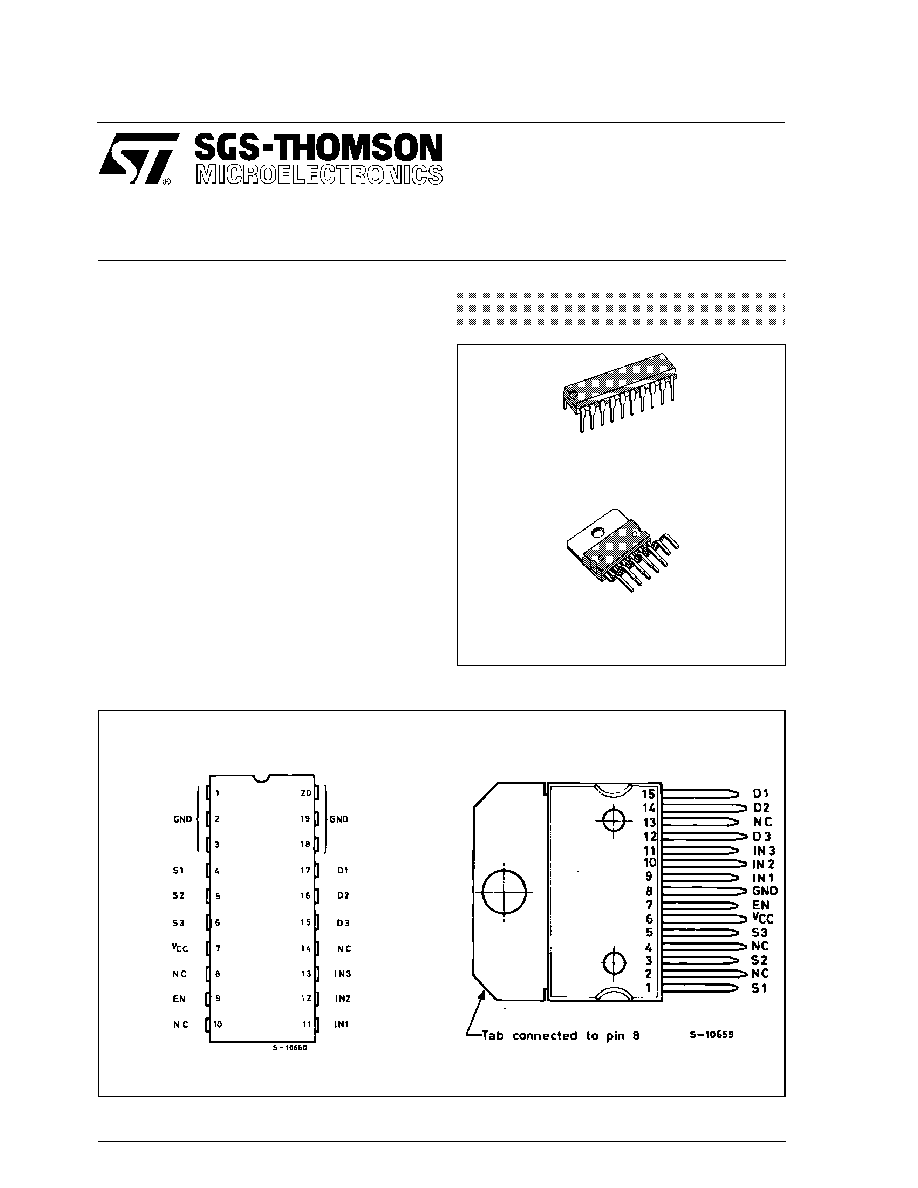
Two versions are available : the L6122 mounted in
a Powerdip 14 + 3 + 3 package and the L6123 in a
15-lead Multiwatt package.
Pow erd ip 14+3+3
(Plastic Package)
ORDERING NUMBER : L6122
1/9
This is advanced information on a new product now in development or undergoing evaluation. Details are subject to change without notice.
MULTI WATT15V
(Plastic Package)
ORDERING NUMBER : L6123
PIN CONNECTIONS (top view)
L6122 (PO WERDI P)
L6123 (MULTI WATT15V)
MULTIPOWER BCD TECHNOLOGY
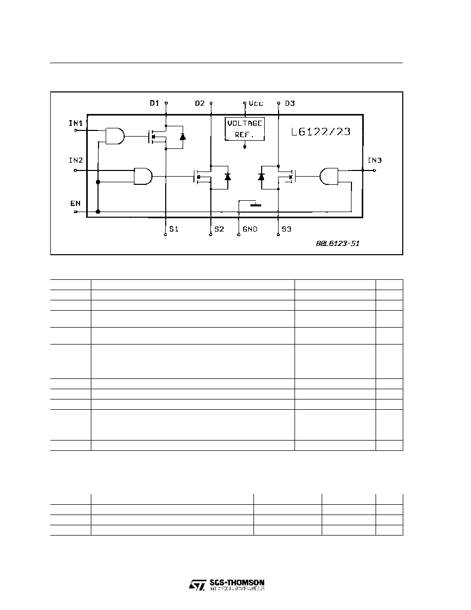
BLOCK DIAGRAM
ABSOLUTE MAXIMUM RATINGS
Symbol
Parameter
Value
Unit
V
DS
Drain-source Voltage
100
V
V
CC
Supply Voltage
60
V
I
D
Continuous Drain Current @ T
pins
= 90
∞
C, POWERDIP
@ T
case
= 90
∞
C, MULTIWATT
1.5
3
A
A
I
DM
(*)
Pulsed Drain Current
POWERDIP
MULTIWAT T
5
8
A
A
I
SD
Continuous Source-drain
@ T
pins
= 90
∞
C, POWERDIP
Diode Current
@ T
case
= 90
∞
C, MULTIWATT
1.5
3
A
A
I
SDM
Pulsed Source Drain Diode Current
POWERDIP
MULTIWATT
5
8
A
A
V
IN
Input Voltage
7
V
V
EN
Enable Voltage
7
V
V
S
Source Voltage
≠ 1 to + 4
V
P
tot
Total Power Dissipation
@ T
pins
= 90
∞
C, POWERDIP
@ T
case
= 90
∞
C, MULTIWATT
@ T
amb
= 70
∞
C, POWERDIP
@ T
amb
= 70
∞
C, MULTIWATT
4.3
20
1.3
2.3
W
W
W
W
T
stg
, T
j
Storage and Junction Temperature Range
≠ 40 to + 150
∞
C
(*) Pulse width
300
µ
s, duty cycle
10 %.
NOTE : I
D
, I
DM
, I
SD
, I
SDM
are given per channel.
THERMAL DATA
Symbol
Parameter
POWERDIP14+3+3
MULTIW ATT15
Unit
R
th j-pins
Thermal Resistance Junction-pins
Max.
14
-
o
C/W
R
th j-case
Thermal Resistance Junction-case
Max.
-
3
o
C/W
R
th j-amb
Thermal Resistance Junction-ambient
Max.
65
35
o
C/W
L6122 - L6123
2/9
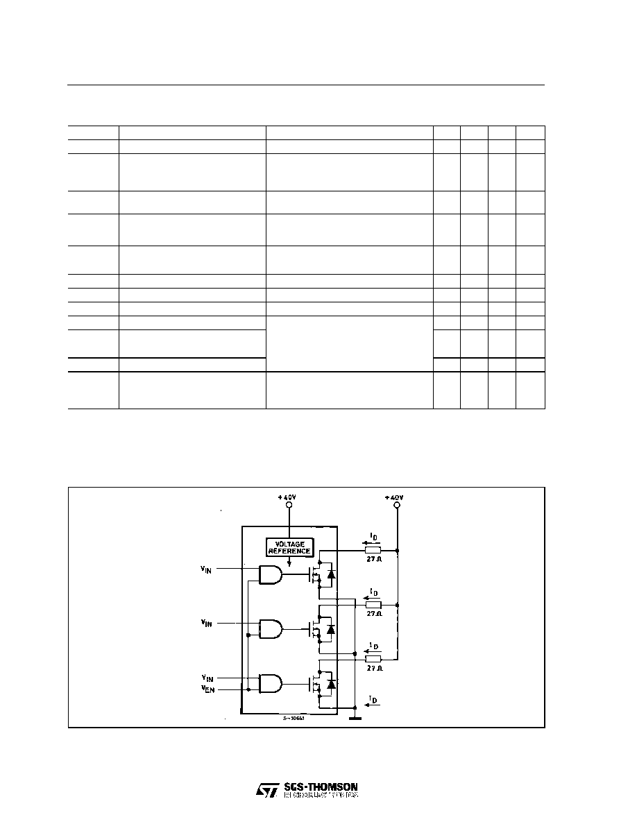
SWITCHING TIMES RESISTIVE LOAD
Figure 1 : Test Circuit.
ELECTRICAL CHARACTERISTICS (T
j
= 25
o
C, V
CC
= 40V, unless otherwise specified)
Symbol
Parameter
Test Conditions
Min.
Typ. Max.
Unit
V
CC
Supply Voltage
14
48
V
I
CC
Supply Current
All V
IN
= H
V
EN
= Square Wave (200kHz, 50% DC)
9
mA
I
Q
Quiescent Current
V
EN
= L
2
3
mA
BV
DSS
Drain Source Breakdown Voltage
I
D
= 1mA
V
EN
= L
100
V
I
DSS
Output Leakage Current
V
EN
= L
V
DS
= 100V
V
DS
= 80V, T
j
= 125
∞
C
1
1
mA
R
DS(on)
(*)
Static Drain-source on Resistance
V
CC
14V, I
D
= 1.5A - V
EN
, V
IN
= H
0.7
V
INL
, V
ENL
Input Low Voltage
- 0.3
0.8
V
V
INH
, V
ENH
Input High Voltage
2
7
V
I
INL
, I
ENL
Input Low Current
V
IN
, V
EN
= L
- 100
µ
A
I
INH
, I
ENH
Input High Current
V
IN
, V
EN
= H
10
µ
A
t
d (on)
Turn on Delay Time
I
D
= 1.5A
See Test Circuit and Waveforms
300
ns
t
r
Rise Time
100
ns
t
d (off )
Turn off Delay Time
400
ns
t
f
Fall Time
100
ns
V
SD
(*)
Source Drain Diode Forward
Voltage
I
SD
= 1.5A, V
EN
= L
1.5
V
V
SD(on)
(*)
Source Drain Forward Voltage
I
SD
= 1.5A - V
IN
, V
EN
= H
1.2
V
(*) Pulse test : pulse width = 300
µ
s, duty cycle = 2 %.
L6122 - L6123
3/9
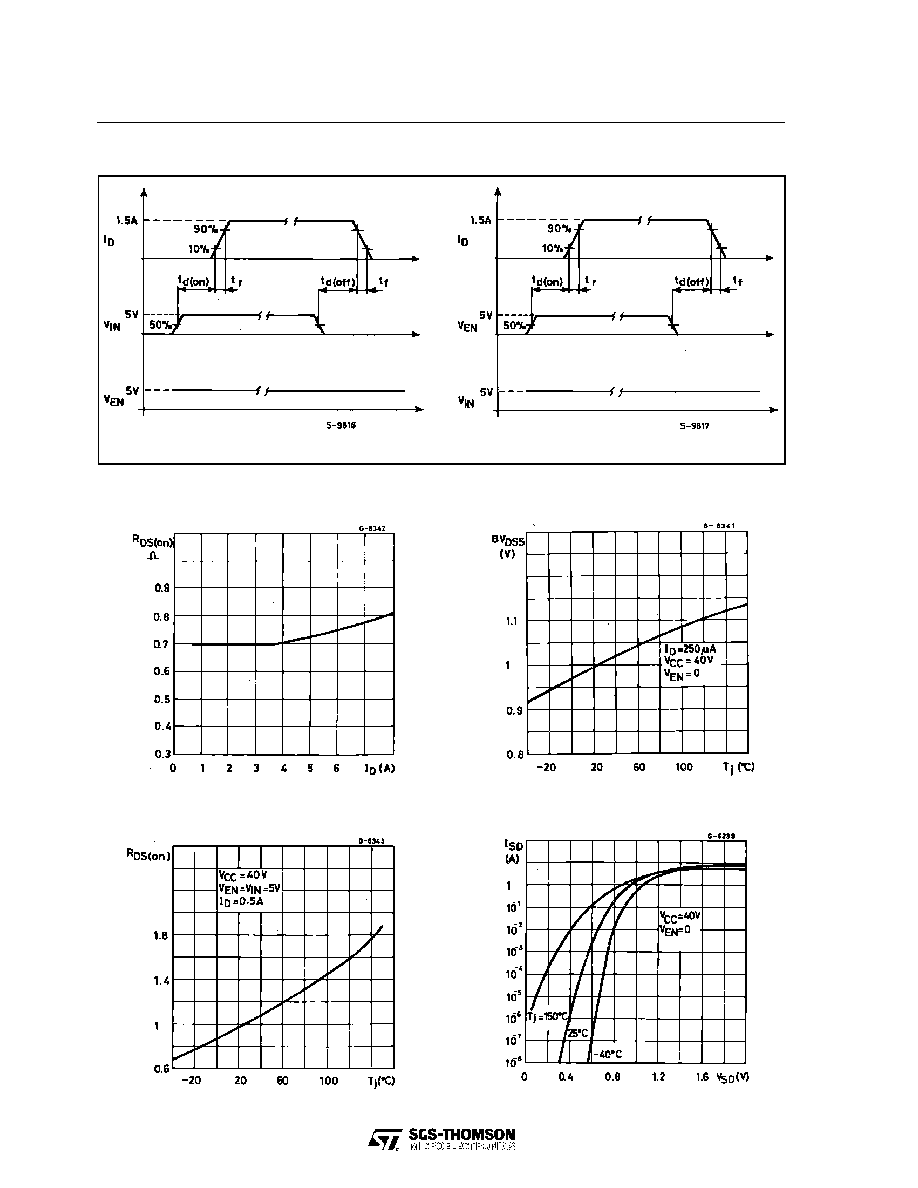
Figure 2 : Waveforms.
a)
b )
Figure 3 : Static Drain-source on Resistance.
Figure 4 : Normalized Breakdown Voltage vs.
Temperature.
Figure 5 : Normalized on Resistance vs. Tempe-
rature.
Figure 6 : Typical Source-drain Diode Forward
Voltage.
L6122 - L6123
4/9
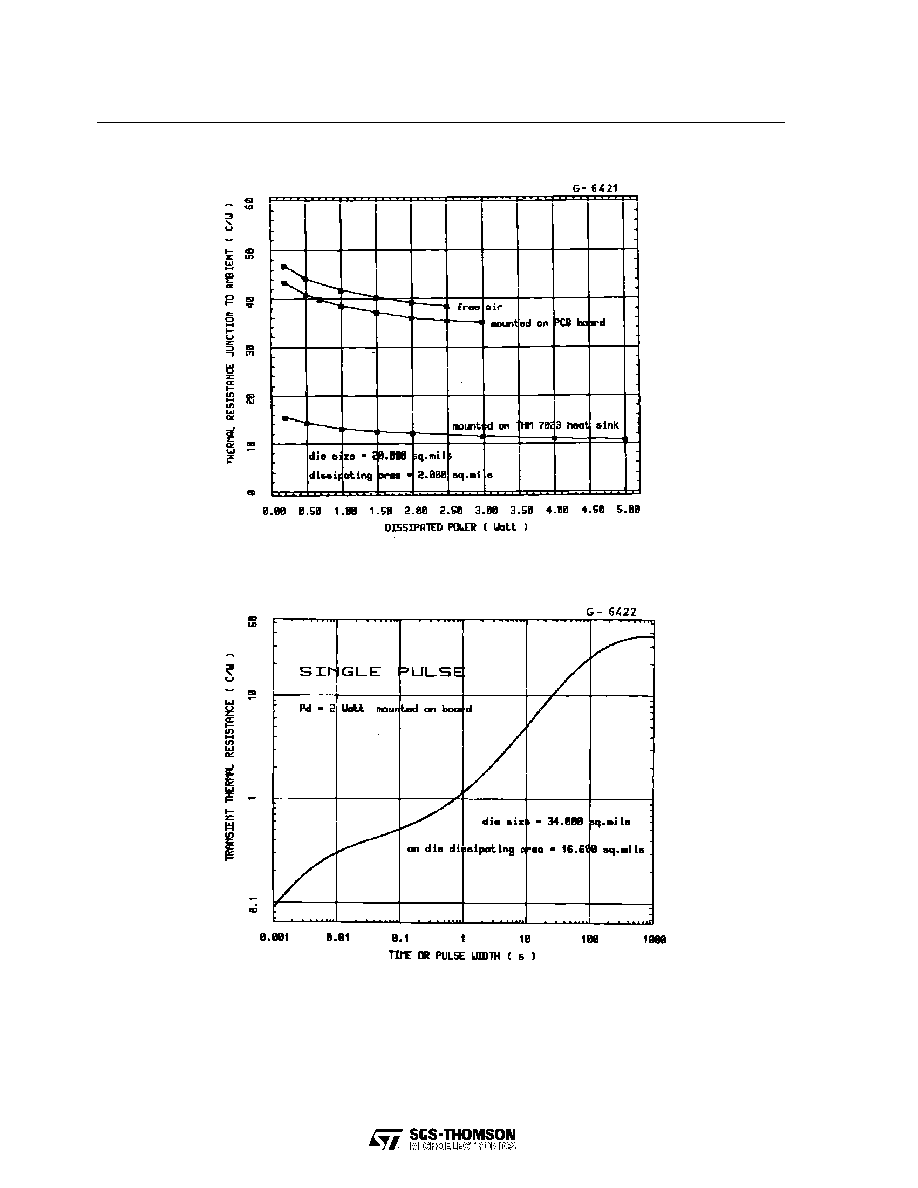
Figure 7 : R
th j-amb
vs. Dissipated Power (Multiwatt).
(*) Rth
9
∞
C/W
Figure 8 : Transient Thermal Resistance for Single Pulses (Multiwatt).
L6122 - L6123
5/9
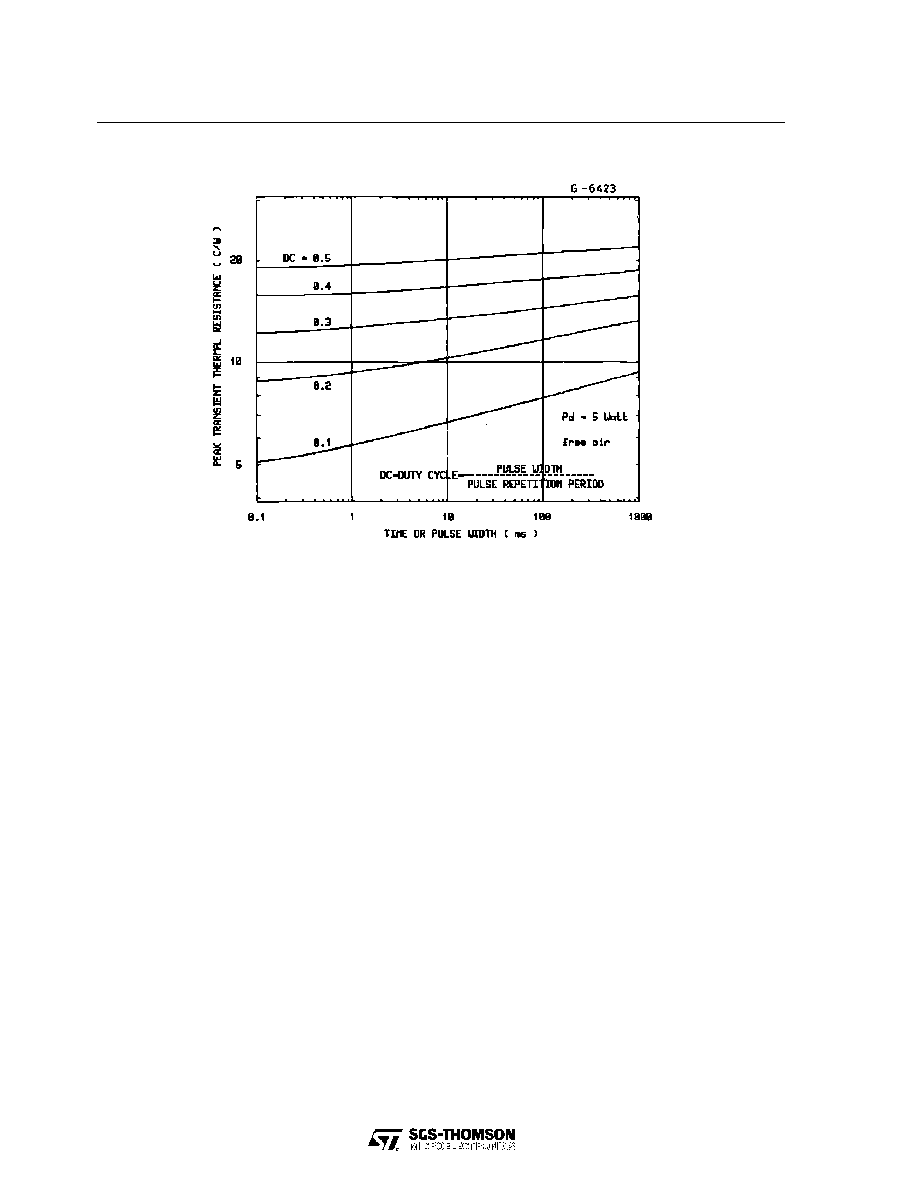
Figure 9 : Peak Transient Thermal Resistance vs. Pulse Width and Duty Cycle (Multiwatt).
L6122 - L6123
6/9
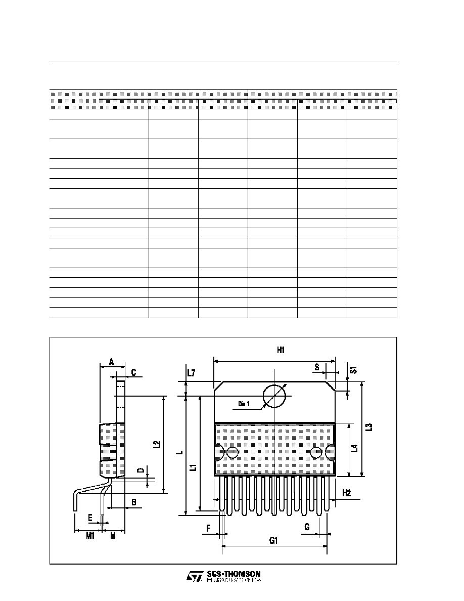
MULTIWATT15 PACKAGE MECHANICAL DATA
DIM.
mm
inch
MIN.
TYP.
MAX.
MIN.
TYP.
MAX.
A
5
0.197
B
2.65
0.104
C
1.6
0.063
D
1
0.039
E
0.49
0.55
0.019
0.022
F
0.66
0.75
0.026
0.030
G
1.14
1.27
1.4
0.045
0.050
0.055
G1
17.57
17.78
17.91
0.692
0.700
0.705
H1
19.6
0.772
H2
20.2
0.795
L
22.1
22.6
0.870
0.890
L1
22
22.5
0.866
0.886
L2
17.65
18.1
0.695
0.713
L3
17.25
17.5
17.75
0.679
0.689
0.699
L4
10.3
10.7
10.9
0.406
0.421
0.429
L7
2.65
2.9
0.104
0.114
M
4.2
4.3
4.6
0.165
0.169
0.181
M1
4.5
5.08
5.3
0.177
0.200
0.209
S
1.9
2.6
0.075
0.102
S1
1.9
2.6
0.075
0.102
Dia1
3.65
3.85
0.144
0.152
L6122 - L6123
7/9
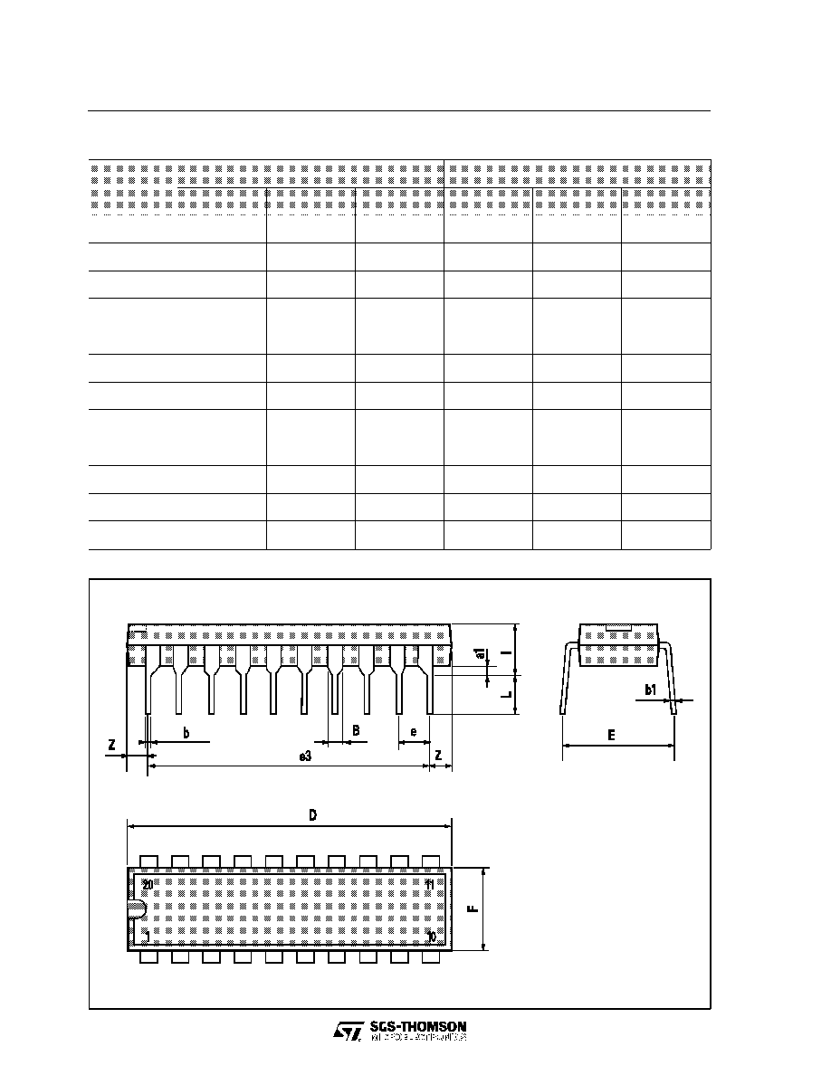
POWERDIP20 PACKAGE MECHANICAL DATA
DIM.
mm
inch
MIN.
TYP.
MAX.
MIN.
TYP.
MAX.
a1
0.51
0.020
B
0.85
1.40
0.033
0.055
b
0.50
0.020
b1
0.38
0.50
0.015
0.020
D
24.80
0.976
E
8.80
0.346
e
2.54
0.100
e3
22.86
0.900
F
7.10
0.280
I
5.10
0.201
L
3.30
0.130
Z
1.27
0.050
L6122 - L6123
8/9

Information furnished is believed to be accurate and reliable. However, SGS-THOMSON Microelectronics assumes no responsibility for
the consequences of use of such information nor for any infringement of patents or other rights of third parties which may result from its
use. No license is granted by implication or otherwise under any patent or patent rights of SGS-THOMSON Microelectronics. Specifica-
tions mentioned in this publication are subject to change without notice. This publication supersedes and replaces all information pre-
viously supplied. SGS-THOMSON Microelectronics products are not authorized for use as critical components in life support devices or
systems without express written approval of SGS-THOMSON Microelectronics.
©
1994 SGS-THOMSON Microelectronics - All Rights Reserved
MULTIWATT
Æ
is a Registered Trademark of SGS-THOMSON Microelectronics
SGS-THOMSON Microelectronics GROUP OF COMPANIES
Australia - Brazil - France - Germany - Hong Kong - Italy - Japan - Korea - Malaysia - Malta - Morocco - The Netherlands - Singapore -
Spain - Sweden - Switzerland - Taiwan - Thaliand - United Kingdom - U.S.A.
L6122 - L6123
9/9