 | –≠–ª–µ–∫—Ç—Ä–æ–Ω–Ω—ã–π –∫–æ–º–ø–æ–Ω–µ–Ω—Ç: L6223 | –°–∫–∞—á–∞—Ç—å:  PDF PDF  ZIP ZIP |

March 1998
BLOCK DIAGRAM
POWERDIP
16+2+2
MULTIPOWER BCD TECHNOLOGY
ORDERING NUMBER : L6223
L6223
DMOS PROGRAMMABLE
HIGH SPEED UNIPOLAR STEPPER MOTOR DRIVER
HIGH EFFICIENCY UNIPOLAR STEPPER
MOTOR DRIVER
HIGH SPEED UNIPOLAR STEPPER MOTOR
DRIVER
SUPPLY VOLTAGE UP TO 46V
PHASE CURRENT UP TO 1A
UP TO 2A/PHASE IN DUAL CONFIGURA-
TION
PARALLEL CMOS
µ
P INTERFACE FOR
FULL/HALF STEP MOTOR ROTATION
SERIAL INTERFACE FOR 6 BIT PROGRAM-
MING
CLOSE/OPEN LOOP, 8 PWM CURRENT
LEVELS
DUAL PWM FREQUENCY SELECTION
INPUT BIDIRECTIONALLY PROTECTED
THERMAL SHUTDOWN
DESCRIPTION
The L6223 is a programmable integrated system
for driving a unipolar stepper motor. It is realized
in Multipower BCD technology. The DMOS output
stage, realized by a single upper DMOS switch
and four lower DMOS, can deliver up to 1A/phase
with motor supply voltages up to 46V.
All inputs are CMOS and microprocessor compat-
ible. An internal 6-bit shift register allows the de-
vice to be programmed to select different duty cy-
cles in open loop mode and different chopping
frequencies in closed loop mode. When the cur-
rent control is in closed loop mode it is also possi-
ble to select a reduced current chopping level to
optimize system efficiency. The L6223 is de-
1/33
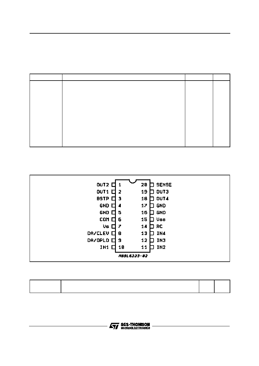
PIN CONNECTION ( top wiew )
signed to work with a single sense resistor. Dur-
ing chopping t(OFF) time the current is reduced
by half, improving efficiency. Higher current appli-
cations can be achieved by paralleling two L6223.
The L6223 is mounted in a 20-lead Powerdip
package, (16+2+2). Four ground leads conduct
heat to dedicated heatsink area on the PCB.
Symbol
Parameter
Value
Unit
V
SS
Logic supply
7
V
V
S
Supply voltage
50
V
V
I
Logic input voltage (*)
≠ 0.3V to V
SS
V
O
Output voltage
100
V
V
Opeak
Output peak voltage (tpk = 5
µ
s,10% d.c.)
125
V
I
pl
Output sink peak current d.c. 10% t(on) = 10
µ
s
3
A
I
ph
Output source peak current d.c. 10%,t(on) = 10
µ
s
6
A
P
tot
Total power dissipation: T
pins
= 90
∞
C
4.3
W
T
amb
= 70
∞
C (**)
2
W
V
sense
Sensing voltage
≠ 1V to V
SS
T
stg,
T
j
Storage and junction temperature
≠ 40 to 150
∞
C
( * ) Oscillator running
( ** ) 4 cm
2
copper area on PCB, see fig. 34
ABSOLUTE MAXIMUM RATINGS
R
thj-pins
Thermal Resistance Junction-pins
Max
14
∞
C/W
R
thj-amb
Thermal Resistance Junction-ambient
Max
60
∞
C/W
THERMAL DATA
L6223
2/33

No.
Name
Fun ction
1,2
18,19
OUT2,OUT1
OUT4,OUT3
Outputs for motor windings.
3
BSTP
A bootstrap capacitor connected between this pin and COM will
generate the internal overvoltage required for driving the gate of the
upper DMOS.
6
COM
Output for common wire of motor.
4,5
16,17
GND
Common ground. Also provides heatsinking to PCB.
7
V
S
Power supply
8
DA/CLEV
Digital input.
1) In PROGRAM MODE,operates in XOR with DA/OPLO to load data
into 6-bit shift register.
2) In OPERATING MODE,works with the other digital inputs to reduce
the current level (see Table 2 and Table 3).
9
DA/OPLO
Digital input.
1) In PROGRAM MODE, operates in XOR with DA/CLEV to load data
into 6-bit shift register.
2) In OPERATING MODE,selects current control method: open loop (H)
or closed loop (L).
10,11
12,13
IN1,IN2
IN3,IN4
Digital inputs. When all inputs are low level,the device is in
PROGRAMMING MODE.
In OPERATING MODE:
1) FULL MODE - IN1 to IN4 drive the motor phases.
A previous programming is requested.
2) SIMPLIFIED MODE - IN1 and IN2 drive the phases,IN3 is
ENABLE, IN4 works with DA/CLEV to enable the reduce current
level. Previous programming not needed.
14
RC
Input for external RC network. Defines the higher of two possible
chopping frequencies. If this pin is set to ground it will reset the IC.
15
V
SS
Logic supply.
20
SENSE
Output for sense resistor.
PIN DESCRIPTION
L6223
3/33
ELECTRICAL CHARACTERISTICS (T
j
= 25
∞
C, V
S
= 42V, V
SS
= 5V, external RC network: R = 18k
,
C = 3.3nF, unless otherwise specified).
Symbol
Parameter
Test conditions
Min
Typ
Max
Unit
V
S
Power Supply
9
32
46
V
V
SS
Logic Supply
4.5
5
5.5
V
I
S
Power Supply Quiescent
Current
IN1, IN2, IN3, IN4 = L
RC = 0V DA/CLEV = L
DA/OPLO = L
2
4
mA
I
SS
Logic Supply Quiescent
Current
IN1, IN2, IN3, IN4 = L
RC = 0V DA/CLEV = L
DA/OPLO = L
14
20
mA
I
OL
Output Leakage Curr.
V
O
= 100V (Fig. 1)
1
mA
V
rs
Reset Threshold
Voltage (Pin 14)
0.9
V
T
BOOT
Bootstrap Refresh Pulse
C
BOOT
= 10nF
3
5
µ
s
SINK MOS
R
DS(ON)
ON Resistance
(Fig. 2a and Fig. 3)
1.2
SOURCE MOS
R
DS(ON)
ON Resistance
(Fig. 2b and Fig. 3)
0.7
CURRENT CONTROL SECTION
V
ref
Internal Reference Volt.
DA/CLEV = L; IN4 = H
I
O
= 100% nominal value
0.475
0.5
0.525
V
f
(OSC)
Oscillator Frequency
(Fig. 20)
18
20
22
KHz
t
(dis)
RC Network Discharge
Time (t
ON
min)
(Fig. 20)
2.3
3
4.3
µ
s
R
int
Internal Discharge Resistor
(pin 14)
1.2
k
T
W
Sense Filter Time Constant
(Fig. 4)
1
1.4
2.3
µ
s
LOGIC LEVELS
V
(IN)L
Input Low Voltage
≠0.3
0.8
V
V
(IN)H
Input High Voltage
2.4
V
SS
V
L6223
4/33
ELECTRICAL CHARACTERISTICS (Continued)
Symbol
Parameter
Test conditions
Min
Typ
Max
Unit
SWITCHING TIMING
t2, t4
Fall/Rise Time (IN1, 2, 3, 4)
R
(load)
= 39
(Fig. 5)
Pure Resistive Load to V
S
250
ns
t1, t3
Input-Output Delay
(IN1, 2, 3, 4)
R
(load)
= 39
(Fig. 5)
Pure Resistive Load to V
S
700
ns
t
dPWM
Close Loop PWM
Control Delay
(Fig. 4) Note 1
1
µ
s
PROGRAMMING TIMING
t1
Loading Time
(Fig. 6)
1.7
µ
s
t2
Protection Time
(Fig. 6) Note 2
0.2
µ
s
t3
Data Set-up
(Fig. 6)
0
ns
t4
Data Hold
(Fig. 6)
1.6
µ
s
t5
Setting Time
(Fig. 6)
200
ns
Note 1) Upper DMOS turn ON delay when the signal is applied at the input comparator (point A in Fig. 4).
Note 2) Internal clock pulse is generated only if IN1...IN4 stay Low for almost 0.2
µ
s. This delay avoids undesirable programmings.
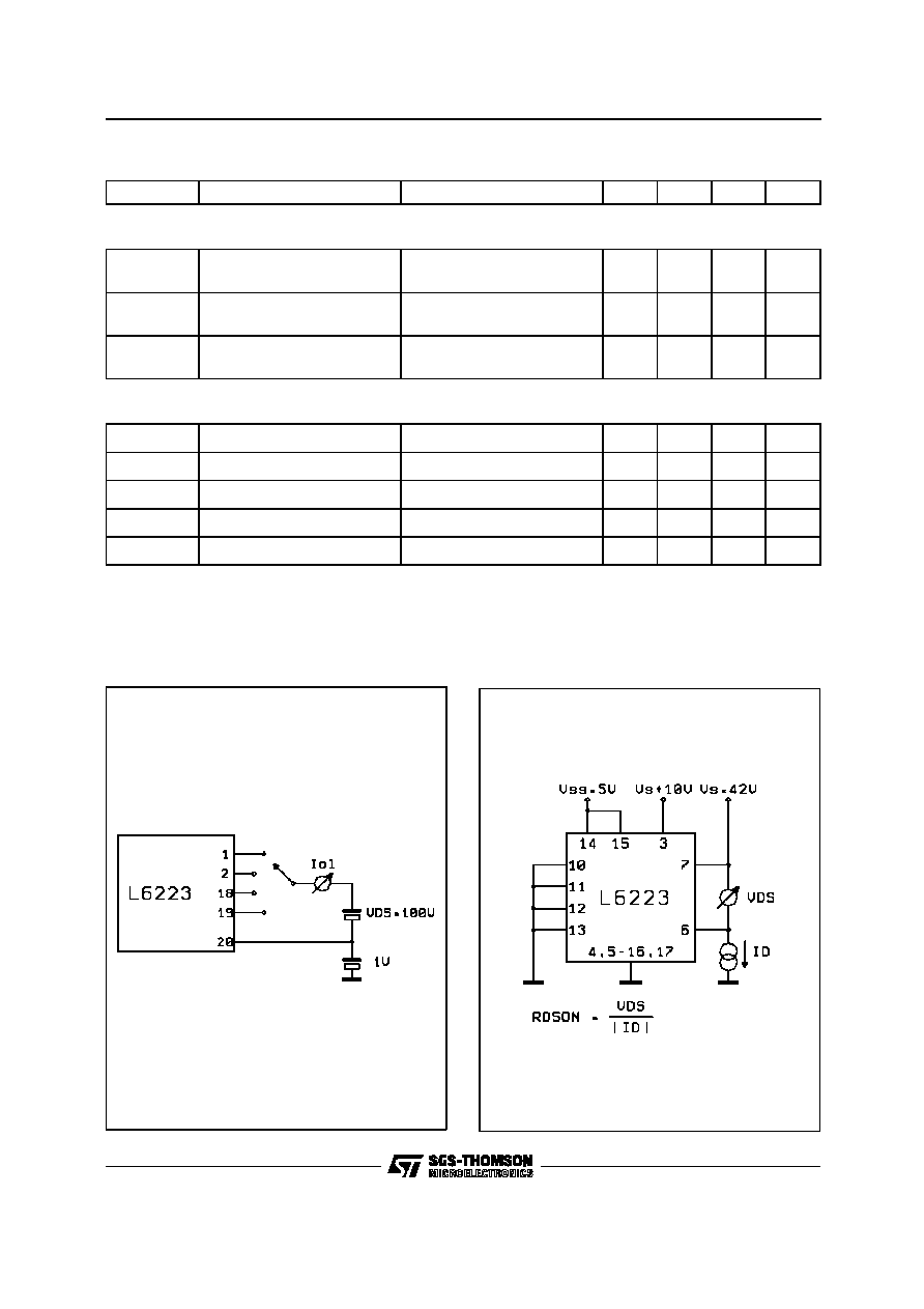
Figure 1: Output leakage I
OL
Test Circuit
Figure 2a: Source Output DMOS R
DS(ON)
Test
Circuit
L6223
5/33