 | –≠–ª–µ–∫—Ç—Ä–æ–Ω–Ω—ã–π –∫–æ–º–ø–æ–Ω–µ–Ω—Ç: L6243 | –°–∫–∞—á–∞—Ç—å:  PDF PDF  ZIP ZIP |
L6243
L6243D
VOICE COIL MOTOR DRIVER
12V/5V OPERATION
PARKING FUNCTION
FOR HARD
DISK
HEAD ACTUATOR
OUTPUT CURRENT UP TO 2A DC, 2.5A
PEAK
LOW SATURATION VOLTAGE
LOGIC AND POWER SUPPLY MONITOR
LINEAR CONTROL
THERMAL PROTECTION
ENABLE FUNCTION
CURRENT SENSE RESISTOR CONNEC-
TIONS
DESCRIPTION
The L6243/D is a Bipolar IC developed for use in
Hard Disk Head Actuator positioning applications.
The Power Op-Amp Output Bridge, Differential
Amplifier, and Error Amplifier, are controlled by
TTL/CMOS, input compatible, Digital Logic, and
an Analog Current Control Voltage. A simple
RC compensation network, tied to the output of
the Error Amp, will configure the system to work
as a Transconductance Amplifier to drive a
Voice Coil Motor in Linear Mode.
Additional features include Power On Reset De-
lay, Enable and Park, as well as a general pur-
pose Operational Amplifier. A logic low at the
Park input activates the parking function. Holding
the Enable input low will disable the device by
forcing the outputs into a tristate mode. Power
Fail Monitors for the logic and power supplies in-
itiate an automatic parking sequence during a
power failure. A resistor programmed parking
voltage enables a constant velocity head retract.
This is advanced information on a new product now in development or undergoing evaluation. Details are subject to change without notice.
July 1996
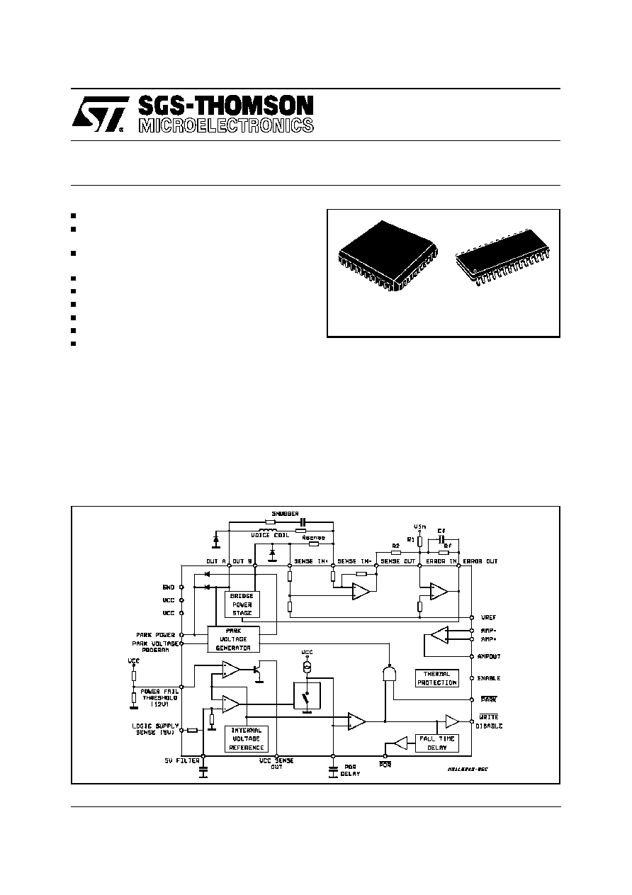
BLOCK DIAGRAM
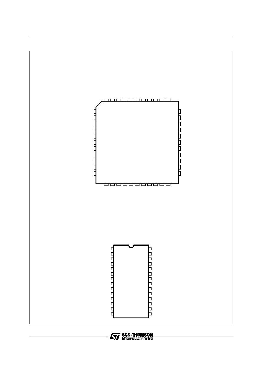
PLCC44
SO(24+2+2)
ORDERING NUMBERS:
L6243
L6243D
1/12
PIN CONNECTION (Top view)
1
2
3
5
6
4
7
8
9
10
12
11
13
14
15
16
17
39
38
37
36
34
35
33
32
31
30
29
40
41
42
44 43
23
22
21
19
18
20
28
27
26
24 25
V
CC
(12V)
V
REF
SENSE
AMP
OUTPUT
N.C.
GND
N.C.
GND
N.C.
SENSE
AMP
INPUT
B
PARK
POWER
OOUTPUT
B
GND
ERROR AMP INPUT
ERROR AMP OUTPUT
OP AMP -INPUT
OP AMP OUTPUT
OP AMP +INPUT
GND
WRITE DISABLE OUTPUT
POWER ON RESET OUTPUT
PARK VOLTAGE PROGRAM
GND
GND
SENSE AMP INPUT A
N.C.
GND
GND
N.C.
N.C.
N.C.
GND
ENABLE INPUT
GND
V
CC
(12V)
LOGIC
SUPPLY
SENSE
(5V)
POWER
ON
REST
DELAY
POWER
FAIL
THRESHOLD
N.C.
V
CC
SENSE
OUTPUT
N.C.
N.C.
PARK
INPUT
5V
FILTER
OUTPUT
A
D96IN449
ERROR OUTPUT
GND
GND
WRITE DISABLE OUTPUT
POWER ON RESET OUTPUT
POWER FAIL THRESHOLD
PARK VOLTAGE PROGRAM
V
CC
SENSE OUTPUT
POWER ON RESET DELAY
1
3
2
4
5
6
7
8
9
LOGIC SUPPLY SENSE (5V)
V
CC
5V FILTER
PARK INPUT
OUTPUT A
ENABLE
GND
GND
SENSE AMP INPUT A
23
22
21
20
19
17
18
16
15
D96IN450
10
11
12
13
14
28
27
26
25
24
V
REF
N.C.
N.C.
N.C.
ERROR AMP INPUT
SENSE AMP INPUT B
OUTPUT B
PARK POWER
V
CC
SENSE AMP OUTPUT
PLCC-44
SO 24+2+2
L6243-L6243D
2/12
ABSOLUTE MAXIMUM RATINGS
Symbol
Parameter
Value
Unit
V
S
Supply Voltage
18
V
V
IN
Input Voltage
0.3V to V
S
V
ID
Differential Input Voltage
±
V
S
I
O
DC Output Current
2
A
I
p
Peak Output Current (non repetitive)
2.5
A
P
tot
Total Power Dissipation (T
amb
= 70
∞
C) for L6243
for L6243D
2
1.2
W
W
T
stg
Storage and Junction Temperature
-55 to +150
∞
C
THERMAL DATA
Symbol
Description
L6243
L6243D
Unit
R
th j-pin
R
th j-amb
R
th j-amb
Thermal Resistance Junction to pin
Thermal Resistance Junction to pin floating in air
Thermal Resistance Junction to pin 16 cm
2
copper area on board
heat sink
12
62
36
14
50
∞
C/W
∞
C/W
∞
C/W
PIN FUNCTIONS
Name
Function
V
CC
Power supply.
GND
Common Ground.
V
ref
Voltage Reference.
ENABLE
Input. Logic low will disable IC.
PARK POWER
Input Power supply for the parking circuit.
CURRENT SENSE OUT
Current sense operational amplifier output.
ERROR AMP IN
Error amplifier inverting input.
ERROR AMP OUT
Error amplifier output.
SENSE IN
±
Input for external sense resistors.
OUT A, B
Outputs of the two Power Operational Amplifiers Connections for Voice coil Motor.
PARK
External input for parking. Low will activate the park procedure.
PARK VOLTAGE PROGRAM
Input to set the park voltage.
POWER FAIL THRESHOLD
Supply monitor threshold setting.
LOGIC SUPPLY SENSE
Logic Supply Sense.
5V FILTER
Capacitor connection to filter the logic supply ripple.
V
CC
SENSE OUT
Power supply failure monitor output.
POR
Power on reset output. Low will signal to the controller the failure of the logic supply.
POR DELAY
Capacitor connection to set the power on reset delay.
WRITE DISABLE
Output for write disable. Low will disable the writing mode.
AMP≠
Inverting input of the additional op amp.
AMP+
Non-inverting input of the additional op amp.
AMPOUT
Output of the additional op amp.
L6243-L6243D
3/12

ELECTRICAL CHARACTERISTICS (V
S
= 12V, T
amb
= 25
∞
C; unless otherwise specified)
Symbol
Parameter
Test Condition
Min.
Typ.
Max.
Unit
V
S
Supply Range
4.5
13.2
V
I
d
Quiescent Drain Current
20
mA
T
j
Thermal Shutdown Junction
Temperature
160
∞
C
ERROR AMPLIFIER
I
b
Input Bias Current
1
µ
A
I
OS
Input Offset Current
300
nA
V
OS
Input Offset Voltage
5
mV
Gv
Large Signal Open Loop Voltage
Gain
65
dB
GBW
Gain Bandwidth
3
MHz
G
min
Minimum Voltage Gain
5
I
O
+
Output Source Current
6
mA
I
O≠-
Output Sink Current
6
mA
SR
Slew-rate
2
V/
µ
s
SENSE AMPLIFIER
R
IN
, V
ref
V
ref Input Impedance
9
K
A
d
Differential Gain
8
V/V
SR
Slew-rate
1
V/
µ
s
GBW
Gain Bandwidth Product
3
MHz
R
in
Sense Input Impedance
1.5
K
CMRR
Common Mode Rejection Ratio
55
dB
POWER OP. AMP.
G
V
Voltage Gain
26
dB
V
d
Total Output Voltage Drop
I
O
= 250mA
I
O
= 500mA
I
O
= 1A
I
O
= 2A
450
750
1.15
2.30
1.5
2.5
mV
mV
V
V
V
off
Offset Voltage on Sense
Resistor
5
mV
BW
Bandwidth on Resistive Load
100
KHz
GENERAL PURPOSE OP-AMP
I
b
Input Bias Current
1
µ
A
I
OS
Input Offset Current
300
nA
V
OS
Input Offset Voltage
5
mV
G
V
Large Signal Open Loop Voltage
Gain
65
dB
GBW
Gain Bandwidth Product
1
MHz
I
O+
Output Source Current
6
mA
I
O≠
Output Sink Current
6
mA
SR
Slew Rate
1
V/
µ
s
L6243-L6243D
4/12

FUNCTIONAL DESCRIPTION
The VCM Driver is controlled via three control sig-
nals, ENABLE, POWER ON RESET, and WRITE
DISABLE. An analog input voltage, ERROR AMP
IN, controls the polarity and amplitude of the VCM
driving current.
Refer to figure two. This diagram is a repre-
sentation of the function of the VCM System.
Note that the signals with the bars represent the
"not
true", or "non asserted" condition. From in -
itial power up, the system is held in the Park
Mode. Upon completion of the POWER UP RE-
SET DELAY the machine moves to Tristate Mode
or Run Mode, depending upon the condition of
the ENABLE input. If ENABLE is asserted, the
machine moves directly to Run Mode. If ENABLE
is not asserted, the machine moves to Tristate
Mode.
POWER ON RESET is an asynchronous output.
Additionally it affects the internal logic as a hard
wired reset and therefore if a supply failure occurs
during Tristate or Run state, the machine moves
directly back to the Park Mode. A WRITE DIS-
ABLE occurs a few to ten microseconds prior to
the POWER ON RESET in order for the system
to halt any read/write activity before a head re-
tract begins.
While in Tristate Mode, the assertion of ENABLE
will move the machine to the Run Mode. Run
Mode will typically be the steady running state.
The deassertion of the ENABLE signal causes
the machine to move into Tristate. If it is desired
to perform an active Parking function, the PARK
input must be driven low by the external hard-
ware, or the the VCM can be driven to the Park
position via the ERROR AMP IN control voltage
ELECTRICAL CHARACTERISTICS (continued)
MONITORS AND CONTROL CIRCUIT
Symbol
Parameter
Test Condition
Min.
Typ.
Max.
Unit
V
t1
Threshold Voltage at Logic
Supply Sense
4.45
4.60
4.75
V
V
t2
Threshold Voltage at Power Fail
Threshold Input
1.375
1.4
1.435
V
HV
t1
Hysteresis on V
t1
50
mV
HV
t2
Hysteresis on Vt2
15
mV
V
ll
Low Level Voltage
Write Disable = 2mA
250
500
mV
Power on Reset = 2mA
250
500
mV
I
e
Enable Input Current
V
i
= 2.4V
100
µ
A
V
i
= 0.4V
≠200
µ
A
I
p
Input Current at Park
V
i
= 2.4V
100
µ
A
V
i
= 0.4V
≠200
µ
A
R
f
Equivalent Input Resistance at
5V Filter Input
6.9
K
V
enl
Enable Low Input Voltage
0.8
V
V
enh
Enable High Input Voltage
2
V
V
ph
Parking Input High Voltage
2
V
V
pl
Parking Input Low Voltage
0.8
V
V
pfl
Power Fail Low Output Voltage
I
l
= 2mA
0.5
V
I
prog
Parking Voltage Program Current
100
µ
A
I
ch
Power On Reset Delay
Capacitor Charging
10
µ
A
T
d
Delay Between Write Disable
and Power on Reset Falling
Edges
4
10
µ
s
L6243-L6243D
5/12

FUNCTIONAL DESCRIPTION (continued)
Function
Description
V
CC
input
This is the Power Supply input.
POWER FAIL
THRESH
Input for the V
CC
supply monitor. The Threshold can be externally set via a voltage divider.
V
CC
SENSE OUT
Output
TTL compatible signal indicating the V
CC
supply has dropped below the POWER FAIL
THRESHOLD.
LOGIC SUPPLY
SENSE input
This input is used to monitor the Five Volt Logic Supply for the external control and other support
IC's. The LOGIC SUPPLY SENSE operates independently of the 12V Power Supply. When a
5V supply failure is detected a POWER ON RESET is generated.
5V FILTER input
This pin allows for the application of filter circuitry in order to avoid false triggering.
PARK POWER
input
This input is used during the Power Down/Power Fail Parking operation. When the supply goes
down, a typical Spindle Driver Circuit automatically tristates its output stages. During this time
the spindle motor spins freely and the stored energy is used to drive the VCM to the park
position. The generated BEMF is rectified and filtered across an external PARKING
CAPACITOR.
PROGRAMMABLE
PARK VOLTAGE
input
Used to set the voltage applied to the VCM during an Automatic Parking Operation.
PARK
input
Logic signal asserted low, activates parking.
POWER ON
RESET output
Indicates an error condition to the external control and support circuitry. A Logic Supply Fail
condition automatically initiates a POWER ON RESET. Internal 30k Pullup to LSS.
POWER ON
RESET DELAY
input
The intent of this input is to provide a time delay at power up. During this time, the POWER ON
RESET line will be asserted (low). A POWER ON RESET, will hold the system in the PARK
mode.
Once the delay has timed out, the POWER ON RESET will be removed to allow the
external system to assume control. When applied in a Disk Drive Application, the POWER ON
RESET DELAY will be required to have a minimum duration which will ensure that the
Read/Write Heads can be fully parked.
WRITE DISABLE
output
Becomes asserted a few microseconds prior to the assertion of POWER ON RESET.
Internal 30k Pullup to LSS.
ENABLE
input
This signal originates at the external controller and, when asserted, allows the VCM Drivers to
operate. When deasserted the VCM Driver is forced into Tristate mode. During a POWER ON
RESET condition however, the parking operation is automatic and takes priority over the
ENABLE function. Only at the end of the POWER ON RESET DELAY will the ENABLE input
become active. If active parking is desired, it will be accomplished under control of the V
IN
signal, otherwise it is an automatic function at power down.
V
REF
input
The reference voltage input is basically that voltage, at which the output current is zero.
ERROR AMP IN
input
Inverting input of error amplifier. The non inverting one is internally tied to V
ref
.
Open collector output.
ERROR AMP OUT
output
Error amplifier output pin.
OUTPUT A power
output
Voice Coil power output.
OUTPUT B power
output
Voice Coil power output.
SENSE AMP IN
A/B
signal input
Sense amplifier input pins. The sense resistor is connected across these pins.
SENSE AMP OUT
signal output
Output pin of sense amplifier.
AMPOUT
output
Output of an internal op-amp for general application.
AMP+ input
General purpose op-amp non inverting input.
AMP- input
General purpose op-amp inverting input.
L6243-L6243D
6/12

BLOCK DESCRIPTION
OUTPUT STAGE
It consists of two Power Op Amps connected in
bridge configuration.
CURRENT SENSE AMPLIFIER
Differential amplifier whose inputs are connected
to the sense lines and whose output is accessible
externally. Closing the loop will transform the
differential voltage signal from the sense lines into
a current signal for the Error Amplifier.
ERROR AMPLIFIER
Error amplifier which drives the output stage. The
input and the output pins are accessible exter-
nally.
POWER SUPPLY MONITOR OPERATION
The circuit monitors the logic supply voltage input
(typ 5V) and activates Power on Reset and Write
Disable output when such a supply drops below
the safe operating limit. After the logic supply volt-
age reaches its nominal value a delay capacitor
has to be charged [Tdelay=3x10e5 x C sec] be-
fore Power on Reset and Write Disable outputs
change from low to high level. Falling edges of
Write Disable and Power on Reset are delayed
(typ 4
µ
s) in order to disable the writing on the disk
before the Power on Reset is activated. An addi-
tional supervisor circuit is present in the IC with a
programmable threshold, which is set by an exter-
nal resistive divider. The TTL compatible output
can be used separately or connected to Park in-
put in order to park the head.
The V
CC
sense output pin can also be connected
to 5V filter input in order to implement a POWER
ON RESET function sensitive both to 5V and V
CC
.
PARKING CIRCUIT OPERATIONT
The voice coil driver is switched into the parking
condition when Power on Reset output or Park in-
put are low. In such a condition a fixed voltage is
superimposed on the load and the value of such a
voltage is set by connecting an external resistor
between
Park
Voltage
Program
input
and
ground: (Vpark=Rext x Iref, Iref=100
µ
A typ). Con-
necting ENABLE input to GND the driver will be
disabled (outputs in high impedance mode).
THERMAL SHUTDOWN
It will disable the IC when the junction tempera-
ture exceeds the threshold value above which the
device could be damaged.
Figure 1: Application Circuit (The pinout refers to the L6243)
L6243-L6243D
7/12
Figure 2: Waveforms
L6243-L6243D
8/12
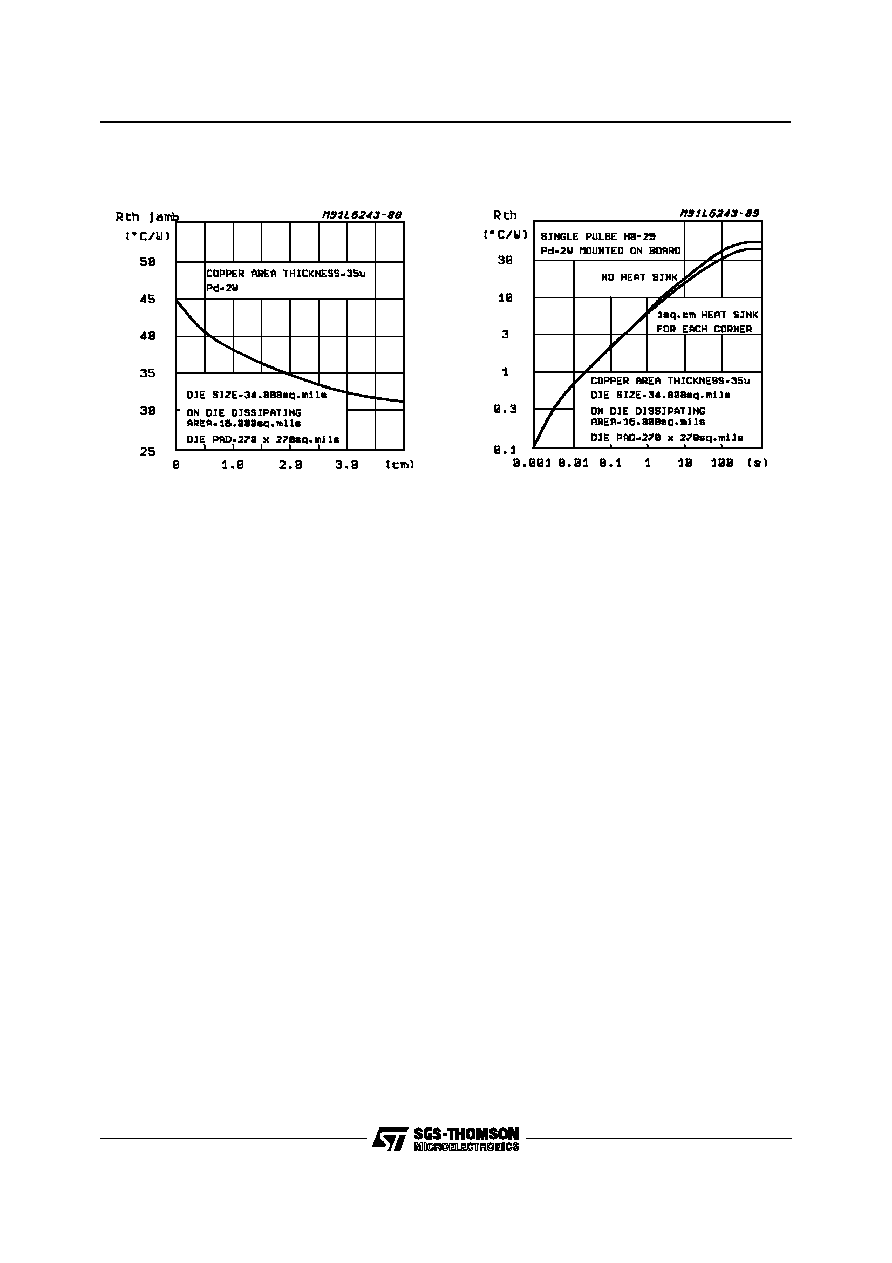
THERMAL CHARACTERISTICS
Figure 3: R
th (j-amb)
vs. Dissipated Power
Figure 4: R
th (j-amb)
vs. Dissipated Power
L6243-L6243D
9/12
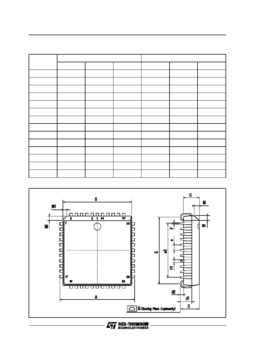
PLCC44 PACKAGE MECHANICAL DATA
DIM.
mm
inch
MIN.
TYP.
MAX.
MIN.
TYP.
MAX.
A
17.4
17.65
0.685
0.695
B
16.51
16.65
0.650
0.656
C
3.65
3.7
0.144
0.146
D
4.2
4.57
0.165
0.180
d1
2.59
2.74
0.102
0.108
d2
0.68
0.027
E
14.99
16
0.590
0.630
e
1.27
0.050
e3
12.7
0.500
F
0.46
0.018
F1
0.71
0.028
G
0.101
0.004
M
1.16
0.046
M1
1.14
0.045
L6243-L6243D
10/12
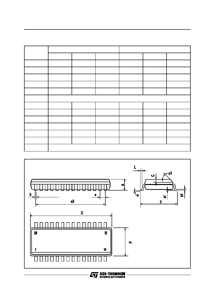
SO28 PACKAGE MECHANICAL DATA
DIM.
mm
inch
MIN.
TYP.
MAX.
MIN.
TYP.
MAX.
A
2.65
0.104
a1
0.1
0.3
0.004
0.012
b
0.35
0.49
0.014
0.019
b1
0.23
0.32
0.009
0.013
C
0.5
0.020
c1
45
∞
(typ.)
D
17.7
18.1
0.697
0.713
E
10
10.65
0.394
0.419
e
1.27
0.050
e3
16.51
0.65
F
7.4
7.6
0.291
0.299
L
0.4
1.27
0.016
0.050
S
8
∞
(max.)
L6243-L6243D
11/12

Information furnished is believed to be accurate and reliable. However, SGS-THOMSON Microelectronics assumes no responsibility for the
consequences of use of such information nor for any infringement of patents or other rights of third parties which may result from its use. No
license is granted by implication or otherwise under any patent or patent rights of SGS-THOMSON Microelectronics. Specification mentioned
in this publication are subject to change without notice. This publication supersedes and replaces all information previously supplied.
SGS-THOMSON Microelectronics products are not authorized for use as criticalcomponents in life support devices or systems without express
written approval of SGS-THOMSON Microelectronics.
©
1996 SGS-THOMSON Microelectronics ≠ Printed in Italy ≠ All Rights Reserved
SGS-THOMSON Microelectronics GROUP OF COMPANIES
Australia - Brazil - Canada - China - France - Germany - Hong Kong - Italy - Japan - Korea - Malaysia - Malta - Morocco - The Netherlands -
Singapore - Spain - Sweden - Switzerland - Taiwan - Thailand - United Kingdom - U.S.A.
L6243-L6243D
12/12