 | –≠–ª–µ–∫—Ç—Ä–æ–Ω–Ω—ã–π –∫–æ–º–ø–æ–Ω–µ–Ω—Ç: L6271 | –°–∫–∞—á–∞—Ç—å:  PDF PDF  ZIP ZIP |
90V BCD MIXED TECHNOLOGY
SO24 AND SO20 PLASTIC SMD PACKAGE
4.5 TO 13.2V OPERATIVE VOLTAGE
±
25 TO
±
40V OUTPUT VOLTAGE RANGE
SELECTABLE BY EXTERNAL RESISTOR
FULL-WAVE
RESONANT
DC-DC
CON-
VERTER USING SINGLE COIL FOR DUAL
HIGH VOLTAGE GENERATOR WITH OUT-
PUT SLEW RATE CONTROL AND SELF
CURRENT LIMITING
LINEAR MODE AND BANG-BANG MODE
±
40V OR 0/+80V OPERATIVE VOLTAGE
DRIVING CONFIGURATION MODES:
1. SINGLE ENDED VOLTAGE MODE
2. DIFFERENTIAL VOLTAGE MODE
3. SINGLE ENDED CHARGE MODE
DOUBLE OPERATIONAL AMPLIFIERS WITH
500KHZ GAIN BANDWIDTH PRODUCT AND
LOAD DRIVING CAPABILITY FROM 0.4NF
UP TO 24NF
2.5V VOLTAGE REFERENCE
2.5V ANALOG SHIFTING CIRCUITRY
POWER SAVING SLEEP MODE
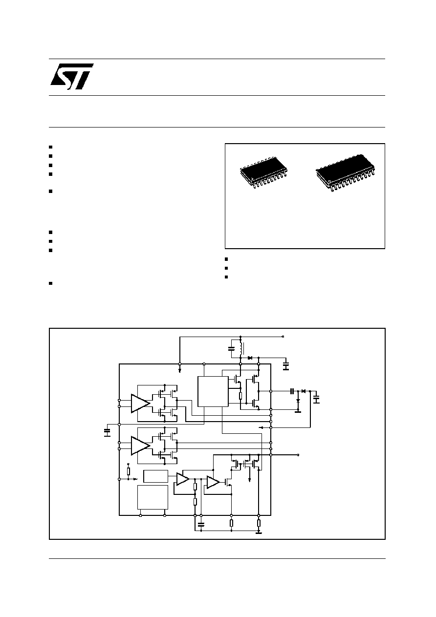
DESCRIPTION
The L6270/1 is a piezoelectric actuator driver.
This is preliminary information on a new product now in development. Details are subject to change without notice.
February 1999
Æ
COIL
+
-
+
-
RESONANT
DC-DC
STEP-UP
CONTROLLER
HVP
HVM
HVP
HVM
1
1
1
1
K
K
K
K
2.5V
50K
SLEEP
ANALOG LEVEL
SHIFTER
VOUT=VIN-2.5
VOUT
VIN
BAND-GAP
REFERENCE
+
-
+
-
INTERNAL
CURRENT
BIAS
100
µ
A
VSUPPLY
200
µ
A
VSUPPLY
4.5V-13V
CRES
BANG-LIN
V512-AP
COIL
HVP
POWER
SUPPLY
INB-
3
21
20
24
17
INB+
16
RC
COMP
22
INA-
8
INA+
9
SLEEP
7
11
10
V-SHIFTED
VIN0-5
13
12
GND-A
VREF
100nF
25K
14
IREF
15
DC2REF
RREFDC
20
5
6
V512A
OUT1-A
OUTK-A
23
HVM
OUT1-B
19
18
OUTK-B
GND-P
2
HBRIDGE
1
D98IN959A
+40V
-40V
100nF
47nF
100nF
Vfdb
1
BLOCK DIAGRAM
SO20
SO24
ORDERING NUMBERS:
L6270
L6271
L6270
L6271
MILLI-ACTUATOR DRIVER
PRODUCT PREVIEW
1/10

H-BRIDGE
GND-P
COIL
OUT1-A
OUTK-A
INA(inv)
SLEEP
INA(not inv)
GND-A
DC2ref
INB(not inv)
INB(inv)
OUT1-B
OUTK-B
V512-AP
RC comp
HVM
HVP
1
3
2
4
5
6
7
8
9
18
17
16
15
14
12
13
11
19
10
20
Vref
Iref
D98IN968
PIN CONNECTION (SO20)
PIN FUNCTIONS (SO20)
N.
Name
Description
1
H-BRIDGE
40V Half Bridge output for negative charge pump.
2
GND-P
Power ground.
3
COIL
Coil for positive step up.
4
OUT1-A
Output ampl.A.
5
OUTK-A
Hi current output ampl.A.
6
SLEEP
Sleep mode for stand-by condition (1=SLEEP 0=operative).
7
INA (inv)
Inverting input of A-amplifier.
8
INA (not inv)
Non Inverting input of A-amplifier.
9
GND-A
Analog ground.
10
V
ref
Precise 2.5V reference voltage.
11
I
ref
External resistor for precise internal current reference.
12
DC2ref
Reference voltage for DC-DC converter X20.
13
INB (not inv)
Non Inverting input of B-amplifier.
14
INB (inv)
Inverting input of B-amplifier.
15
OUTK-B
Hi current output ampl.B.
16
OUT1-B
Output ampl.B.
17
V512-AP
Analog&Power voltage supply 5 to 12V.
18
RC comp
DC-DC converter compensation network.
19
HVM
Negative High voltage generated op amp supplier.
20
HVP
Positive High voltage generated op amp supplier.
L6270 - L6271
2/10

H-BRIDGE
GND-P
COIL
N.C.
OUT1-A
SLEEP
OUTK-A
INA(inv)
INA(not inv)
INB(not inv)
INB(inv)
OUTK-B
V512-AP
OUT1-B
LIN/BANG
RC comp
HVM
HVP
1
3
2
4
5
6
7
8
9
22
21
20
19
18
16
17
15
23
10
24
V-SHIFTED
DC2ref
D98IN969
Vin 0-5
Iref
11
14
13
12
GND-A
Vref
PIN CONNECTION (SO24)
PIN FUNCTIONS (SO24)
N.
Name
Description
1
H-BRIDGE
40V Half Bridge output for negative charge pump.
2
GND-P
Power ground.
3
COIL
Coil for positive step up.
4
N.C.
5
OUT1-A
Output ampl.A.
6
OUTK-A
Hi current output ampl.A.
7
SLEEP
Sleep mode for stand-by condition (1=SLEEP 0=operative).
8
INA (inv)
Inverting input of A-amplifier.
9
INA (not inv)
Non Inverting input of A-amplifier.
10
V-SHIFTED
Analog level shifter output Vin-Vref (-2.5 to +2.5 dynamic range)
11
Vin 0-5
Input positive voltage
12
GND-A
Analog ground.
13
V
ref
Precise 2.5V reference voltage.
14
I
ref
External resistor for precise internal current reference.
15
DC2ref
Reference voltage for DC-DC converter X20.
16
INB (not inv)
Non Inverting input of B-amplifier.
17
INB (inv)
Inverting input of B-amplifier.
18
OUTK-B
Hi current output ampl.B.
19
OUT1-B
Output ampl.B.
20
V512-AP
Analog&Power voltage supply 5 to 12V.
21
LIN/BANG
Linear or Bang-bang select pin (V512 = BANG 0 = Linear)
22
RC comp
DC-DC converter compensation network.
23
HVM
Negative High voltage generated op amp supplier.
24
HVP
Positive High voltage generated op amp supplier.
L6270 - L6271
3/10

ELECTRICAL CHARACTERISTICS (All the following parameters are specified @ 27
∞
C and V512 =
12V, unless otherwise specified.)
Symbol
Parameter
Test Condition
Min.
Typ.
Max.
Unit
V
512
Main power supply
4.5
13.2
V
HVP
(1)
Output positive Voltage
Double Supply Voltage
25
40
V
Single Supply Voltage V
512
8
Single Supply Voltage V
512
8
30
25
80
40
V
V
HVM
Output negative voltage
-40
-25
V
HVripple
HVP, HVM ripple
External filter cap. 100nF
Bang-Bang Mode
Linear Mode
2.5
0.8
V
V
DC-DC gain
Ratio of HVP and DC-DC ref.
voltage PIN15
19
20
21
I, hvp
Output current (see figure 1a)
I, hvm
T
op
Time to operating condition
5
ms
F
switch
(2)
Switching Frequency
80
550
kHz
R
ds, on
Boost transistor ON resistance
4
I
boost
Boost transistor current limiting
700
mA
CP-slope
Charge Pump Slope
150
V/
µ
s
I
sleep
Total current in sleep mode
1
mA
V
ref
Reference voltage at PIN13
2.4
2.5
2.6
V
I
vref
Reference voltage output
current
-1
1
mA
V
ref, cap
Filter capacitor at PIN13
10
100
nF
I
ref, res
Resistor at PIN14 for precise
internal current (100
µ
A)
25
k
V
sup
Minimum OpAmp supply
Voltage (HVP if externally
given)
Double Supply
V512
+4
V
Single Supply
V512
+4
V
DC gain
OpAmp DC gain
130
dB
GBW
OpAmp Gain Bandwidth
product
Cload 0.4nF to 24nF
Double Supply Voltage
500
KHz
DCinp
OpAmp Input dynamic voltage
Double supply
-5
5
V
Single supply
1.2
10
V
DC-DC
OFF
DC-DC Converter switched-off
when DC
2
REF voltage lower
than
0.6
V
ABSOLUTE MAXIMUM RATINGS
Symbol
Parameter
Value
Unit
V512
Supply voltage pin 20 referred to Ground
14
V
HVP
Positive high voltage referred to HVM
84
V
HVM
Negative high voltage referred to Ground
-42
V
IN A&B
Amplifier input voltage common mode
±
6
V
Vi
n
o to 5
Level shifts input voltage
-0.5 to +5.5
V
T
amb
Operative Ambient Temperature
-20 to +80
∞
C
T
stg
Storage Temperature
-40 to +125
∞
C
All the voltage value are referred to ground.
L6270 - L6271
4/10

Symbol
Parameter
Test Condition
Min.
Typ.
Max.
Unit
V
out
OpAmp Output dynamic voltage
Capacitive load
HVM
HVP
V
DC, I
bias
OpAmp Bias supply current
(both)
7
mA
I
out
OpAmp Dynamic Output current
-75
75
mA
PSRR,P
OpAmp Positive power supply
rejection ratio
@ 50kHz
TBD
dB
PSRR,N
OpAmp Negative power supply
rejection ratio
@ 50kHz
TBD
dB
C
load
OpAmp Load capacitance
range
Voltage mode Gain min 20dB
0.4
24
nF
C
int
OpAmp Integration capacitance
Charge mode Gain min 20dB
0.4
24
nF
K
OpAmp Current ratio
OUTK/OUT1
9.8
10
10.2
I
err
(3)
OpAmp Ioutk
Iout1 = 0
-10
50
µ
A
V
offset
OpAmp Input offset voltage
±
10
mV
DC
Shift range
Dynamic Shifter
Input Range
1
4
V
Note 1: Selectable by external resistor.
Note 2: Set by external Coil and Capacitor.
Note 3: It will be write after silicon characterization, it's designed for a maximum offset of a few mA.
In charge mode the Piezo is in open loop, and if Cpiezo = 0.4nF with a maximum Current error of
±
5
µ
A the Maximum long time voltage
drift is
±
12mV/
µ
s
ELECTRICAL CHARACTERISTICS (continued)
0
0.004
0.008
0.012
0.016
I
L
(A)
22
26
V
S
(V)
Supply=5V
Supply=8V
D99IN1003
24
28
30
32
34
36
38
Figure 1a. HVP load regulation in single supply
mode".
L6270 - L6271
5/10