 | –≠–ª–µ–∫—Ç—Ä–æ–Ω–Ω—ã–π –∫–æ–º–ø–æ–Ω–µ–Ω—Ç: L6560AD | –°–∫–∞—á–∞—Ç—å:  PDF PDF  ZIP ZIP |
L6560
L6560A
POWER FACTOR CORRECTOR
VERY PRECISE ADJUSTABLE INTERNAL
OUTPUT OVERVOLTAGE PROTECTION
HYSTERETIC START-UP
(I
START-UP
< 0.5mA)
VERY LOW QUIESCENT CURRENT
(< 3.5mA)
INTERNAL START-UP TIMER
TRANSITION MODE OPERATING
TOTEM POLE OUTPUT CURRENT:
±
400mA
DIP8/SO8 PACKAGES
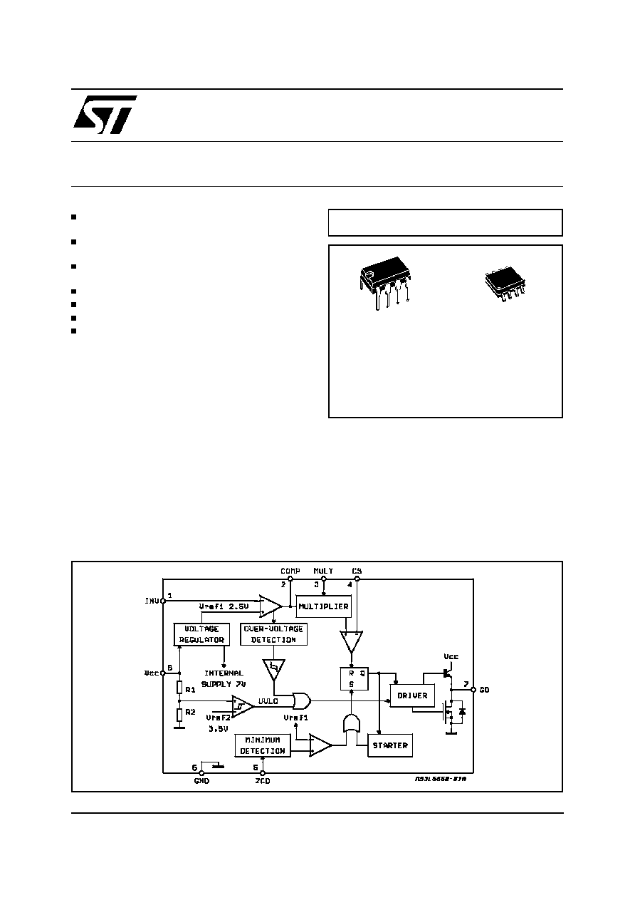
DESCRIPTION
The L6560/A is a monolithic integrated circuit in
Minidip and SO8 packages, designed as a con-
troller and driver of a discrete power MOS transis-
tor for the implementation of active power factor
correction, for sinusoidal line current consump-
tion.
Realized in mixed BCD technology, the chip inte-
grates:
- An undervoltage lockout with micropower start-
up and hysteresis.
- An internal temperature compensated precise
band gap reference.
- A stable error amplifier.
- One quadrant multiplier.
- Current sense comparator.
- An output overvoltage protection circuit.
- A totem-pole output stage able to drive a
POWER MOS or IGBT devices with source
and sink current of 400mA. The chip works in
transition mode and is particularly intended
for lamp ballast applications and for low
power SMPS.
June 2000
Æ
BLOCK DIAGRAM
ORDERING NUMBERS:
L6560
L6560D
L6560A
L6560AD
Minidip
SO8
MULTIPOWER BCD TECHNOLOGY
1/11

ABSOLUTE MAXIMUM RATINGS
Symbol
Pin
Parameter
Value
Unit
I
Vcc
8
I
CC
+ I
Z
30
mA
I
GD
7
Output Totem Pole Peak Current (2
µ
s)
±
700
mA
INV, COMP
MULT
1, 2, 3
Analog Inputs & Outputs
-0.3 to 7
V
CS
4
Current Sense Input
-0.3 to 7
V
ZCD
5
Zero Current Detector
5 (source)
10 (sink)
mA
mA
P
tot
Power Dissipation @T
amb
= 50
∞
C
(Minidip)
(SO8)
1
0.65
W
T
j
Junction Temperature Operating Range
-25 to 150
∞
C
T
stg
Storage Temperature
-55 to 150
∞
C
THERMAL DATA
Symbol
Parameter
SO 8
MINIDIP
Unit
R
th j-amb
Thermal Resistance Junction-ambient
150
100
∞
C/W
PIN FUNCTIONS
N.
Name
Fun ction
1
INV
Inverting input of the error amplifier. A resistive divider is connected between output regulated
voltage and this point, to provide the voltage feedback.
2
COMP
Output of error amplifier. A feedback compensation network is placed between this pin and the
INV pin.
3
MULT
Input of the multipler stage. A resistive divider connects to this pin the rectified mains. A
voltage signal, proportional to the rectified mains, appears on this pin.
4
CS
Input to the comparator of the control loop. The current is sensed by a resistor and the
resulting voltage is applied to this pin.
5
ZCD
Zero current detection input.
6
GND
Ground of the control section.
7
GD
Gate driver output. A push pull output stage is able to drive the Power MOS with peak current
of 400mA (source and sink).
8
V
CC
Supply voltage of driver and control circuits.
PIN CONNECTION
L6560 - L6560A
2/11
ELECTRICAL CHARACTERISTICS (V
CC
= 14.5V; T
j
= 25
∞
C unless otherwise specified)
SUPPLY VOLTAGE SECTION
Symbol
Pin
Parameter
Test Condition
Min.
Typ.
Max.
Unit
V
CC
8
Operating Range
after turn-on
11
18
V
V
CC ON
8
Turn-on Threshold
L6560
L6560A
13.5
11
14.5
12
15.5
13
V
v
V
CC OFF
8
Turn-off Threshold
L6560
L6560A
9
8.7
10
9.6
11
10.5
V
V
Hys
8
Hysteresis
L6560
L6560A
4.3
2.5
4.7
2.8
5.1
3.1
V
V
SUPPLY CURRENT SECTION
Symbol
Pin
Parameter
Test Condition
Min.
Typ.
Max.
Unit
I
START-U
8
Start-up Current
before turn-on at:
V
CC
= 13V (L6560)
V
CC
= 10.5V (L6560A)
0.3
0.5
mA
I
CC
8
Operating Supply Current
C
L
= 0nF @ 70KHz
2.5
3.5
mA
C
L
= 1nF @ 70KHz
3.2
4
mA
in OVP condition V
pin1
= 2.7V
0.9
1.3
mA
V
Z
8
Zener Voltage
I
CC
= 25mA
18
20
22
V
ERROR AMPLIFIER SECTION
Symbol
Pin
Parameter
Test Condition
Min.
Typ.
Max.
Unit
V
INV
1
Voltage Feedback Input
Threshold
2.46
2.5
2.54
V
≠25
T
J
85
∞
C; 12V < V
CC
< 18V
2.43
2.56
T
S
Temperature Stability
T
amb
= -25 to 85
∞
C
0.5
%
R
L
Line Regulation
V
CC
= 11 to 18V
1
4
mV
I
INV
1
Input Bias Current
0.1
1
µ
A
G
V
Voltage Gain
Open loop
60
80
dB
I
COMP
2
Source Current (V
1
< V
ref
)
V
COMP
= 5V
0.14
0.2
mA
Sink Current
(V
1
> V
ref
)
0.5
1
mA
MULTIPLIER SECTION
Symbol
Pin
Parameter
Test Condition
Min.
Typ.
Max.
Unit
V
MULT
3
Operating Voltage
0 to 2.5 0 to 4.2
V
V
CS
V
mult
Output Max. Slope
V
MULT
= from 0V to 1V
V
COMP
= 6V
0.9
1.25
1.6
K
Gain
V
MULT
= 1V V
COMP
= 5V
0.45
0.65
0.85
1/V
CURRENT SENSE COMPARATOR
Symbol
Pin
Parameter
Test Condition
Min.
Typ.
Max.
Unit
V
CS
4
Voltage Threshold
V
MULT
= 2.5V V
COMP
= 6V
1.6
1.9
V
I
CS
4
Input Bias Current
5
µ
A
t
d (H-L)
4
Delay to Output
200
400
ns
L6560 - L6560A
3/11
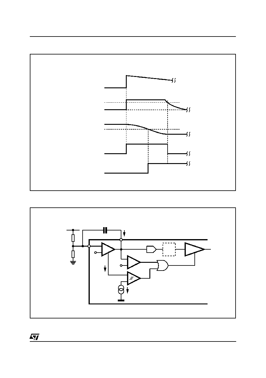
OVER VOLTAGE PROTECTION OVP
The output voltage is expected to be kept by the
operation of the PFC circuits close to its reference
value that is set by the ratio of the two external re-
sistors R
1
and R
2
(see fig. 2), taking into consid-
eration that the non inverting input of the error
amplifier is biased inside the L6560 at 2.5V.
In steady state conditions, the current through R1
and R2 is:
I
SC
=
V
outsc
-
2.5
R1
or I
SC
=
2.5
R2
and, if the external compensation network is
made only with a capacitor C, the current through
C is equal zero.
When the output voltage increases abruptly the
current through R1 becomes:
I
R1
=
V
out
-
2.5
R1
I
R1
=
V
outsc
+
V
OUT
-
2.5
R1
=
I
sc
+
I.
Since the current through R2 doesn't change, the
I current must flow through the capacitor C and
enter in the error amplifier.
This current is mirrored inside the L6560, and
compared with a precise internal reference of
40
µ
A. Whenever such 40
µ
A limit is exceed, the
OVP protection is triggered (Dynamic OVP), and
the external power transistor is switched off, until
the overvoltage situation disappears. However if
the overvoltage persists, before that the transient
condition of dynamic circuit exhausts, an internal
comparator (Static OVP) latches the OVP condi-
tion keeping the external power switch turned off
(see fig. 1).
The OVP value is threfore set by the equation
OVP =
Vout = R
1
40
µ
A.
Typical values for R
1
, R
2
and C are reported in
the application circuit. The overvoltage can be set
independently from the average output voltage.
The precision in setting the overvoltage threshold
is 7% of the overvoltage value (for instance
V =
60V
±
4.2V).
ELECTRICAL CHARACTERISTICS (continued)
ZERO CURRENT DETECTOR
Symbol
Pin
Parameter
Test Condition
Min.
Typ.
Max.
Unit
V
ZCD
5
Input Threshold Voltage Rising
Edge
1.8
2.3
V
Hysteresis
0.3
0.5
0.7
V
V
ZCD
5
Clamp Voltage
I
ZCD
= 3mA
5
5.7
6.4
V
V
ZCD
5
Clamp Voltage
I
ZCD
= ≠3mA
0.4
0.7
1
V
OUTPUT SECTION
Symbol
Pin
Parameter
Test Condition
Min.
Typ.
Max.
Unit
V
GD
7
Dropout Voltage
I
GDsource
= 200mA
1.2
2
V
I
GDsource
= 20mA
0.7
1
V
I
GDsink
= 200mA
1.5
V
I
GDsink
= 20mA
0.3
V
t
r
7
Output Voltage Rise Time
CL = 1nF
50
120
ns
t
f
7
Output Voltage Fall Time
CL = 1nF
40
100
ns
OUTPUT OVERVOLTAGE SECTION
Symbol
Pin
Parameter
Test Condition
Min.
Typ.
Max.
Unit
I
OVP
2
OVP Triggering Current
36
40
44
µ
A
RESTART TIMER
Symbol
Pin
Parameter
Test Condition
Min.
Typ.
Max.
Unit
t
START
Start Timer
45
60
µ
s
L6560 - L6560A
4/11
+Vo
D93IN035B
-
+
2
R1
R2
Ccomp.
E/A
1
2.5V
I
-
+
X
PWM
DRIVER
3.1V
40
µ
A
I
Figure 2: Overvoltage Protection Circuit
V
OUT nominal
I
SC
40
µ
A
E/A OUTPUT
3.1V
DYNAMIC OVP
STATIC OVP
D95IN219A
OVER VOLTAGE
Figure 1.
L6560 - L6560A
5/11