 | –≠–ª–µ–∫—Ç—Ä–æ–Ω–Ω—ã–π –∫–æ–º–ø–æ–Ω–µ–Ω—Ç: L6590A | –°–∫–∞—á–∞—Ç—å:  PDF PDF  ZIP ZIP |

1/19
L6590A
October 2000
s
WIDE-RANGE MAINS OPERATION
s
"ON-CHIP" 700V V
(BR)DSS
POWER MOS
s
65 kHz INTERNAL OSCILLATOR
s
STANDBY MODE FOR HIGH EFFICIENCY AT
LIGHT LOAD
s
OVERCURRENT AND LATCHED
OVERVOLTAGE PROTECTION
s
NON DISSIPATIVE BUILT-IN START-UP
CIRCUIT
s
THERMAL SHUTDOWN WITH HYSTERESIS
s
BROWNOUT PROTECTION
MAIN APPLICATIONS
s
WALL PLUG POWER SUPPLIES UP TO 15W
s
AC-DC ADAPTERS
s
AUXILIARY POWER SUPPLIES FOR:
- CRT AND LCD MONITOR (BLUE ANGEL)
- DESKTOP PC/SERVER
- FAX, TV, LASER PRINTER
- HOME APPLIANCES/LIGHTING
s
LINE CARD, DC-DC CONVERTERS
DESCRIPTION
The L6590A is a monolithic switching regulator de-
signed in BCD OFF-LINE technology, able to operate
with wide range input voltage and to deliver up to
15W output power. The internal power switch is a lat-
eral power MOSFET with a typical R
DS(on)
of 13
and a V
(BR)DSS
of 700V minimum.
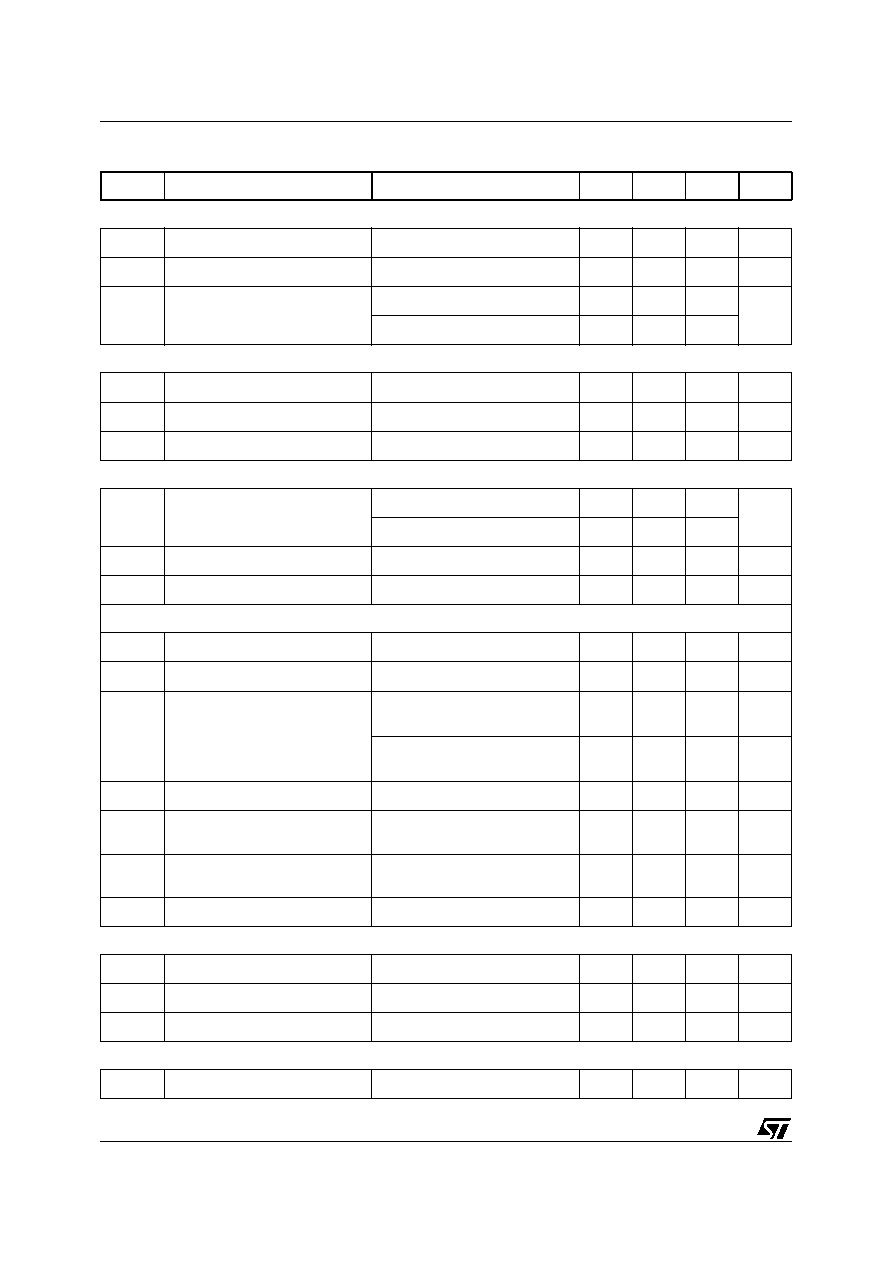
MINIDIP
ORDERING NUMBER: L6590AN
FULLY INTEGRATED POWER SUPPLY
TYPICAL APPLICATION CIRCUIT
3
1
5
6, 7, 8
L6590A
AC line
88 to 264 Vac
4
Vcc
BOK
COMP
DRAIN
GND
Pout
up to 15W

L6590A
2/19
DESCRIPTION (continued)
The MOSFET is source-grounded, thus it is possible
to build flyback, boost and forward converters.
The device is meant to work with secondary feed-
back for tight tolerance of the regulated output volt-
age.
The internal fixed oscillator frequency and the inte-
grated non dissipative start-up generator minimize
the external component count and power consump-
tion.
The device is equipped with a standby function that
automatically reduces the oscillator frequency from
65 to 22 kHz under light load conditions to enhance
efficiency (P
in
< 1W @ P
out
= 0.5W with wide range
mains).
Internal protections like cycle-by-cycle current limit-
ing, latched output overvoltage protection, mains un-
dervoltage
protection
and
thermal
shutdown
generate a 'robust' design solution.
The IC uses a special leadframe with the ground pins
(6, 7 and 8) internally connected in order for heat to
be easily removed from the silicon die. An heatsink
can then be realized by simply making provision of
few cm
2
of copper on the PCB. Furthermore, the pin
close to the high-voltage one is not connected to
ease compliance with safety distances on the PCB.
BLOCK DIAGRAM
PIN CONNECTIONS (Top view)
SUPPLY
& UVLO
OVER
VOLTAGE
OVER
CURRENT
+
-
+
-
2.5V
+
-
DRAIN
(1)
VCC
(3)
BOK
(5)
COMP
(4)
GND
(6,7,8)
VREF
1 mA
BROWNOUT
PWM
STANDBY
START-UP
OSC
65/22 kHz
THERMAL
S.DOWN
BOK
DRAIN
N.C.
Vcc
COMP
GND
GND
GND

3/19
L6590A
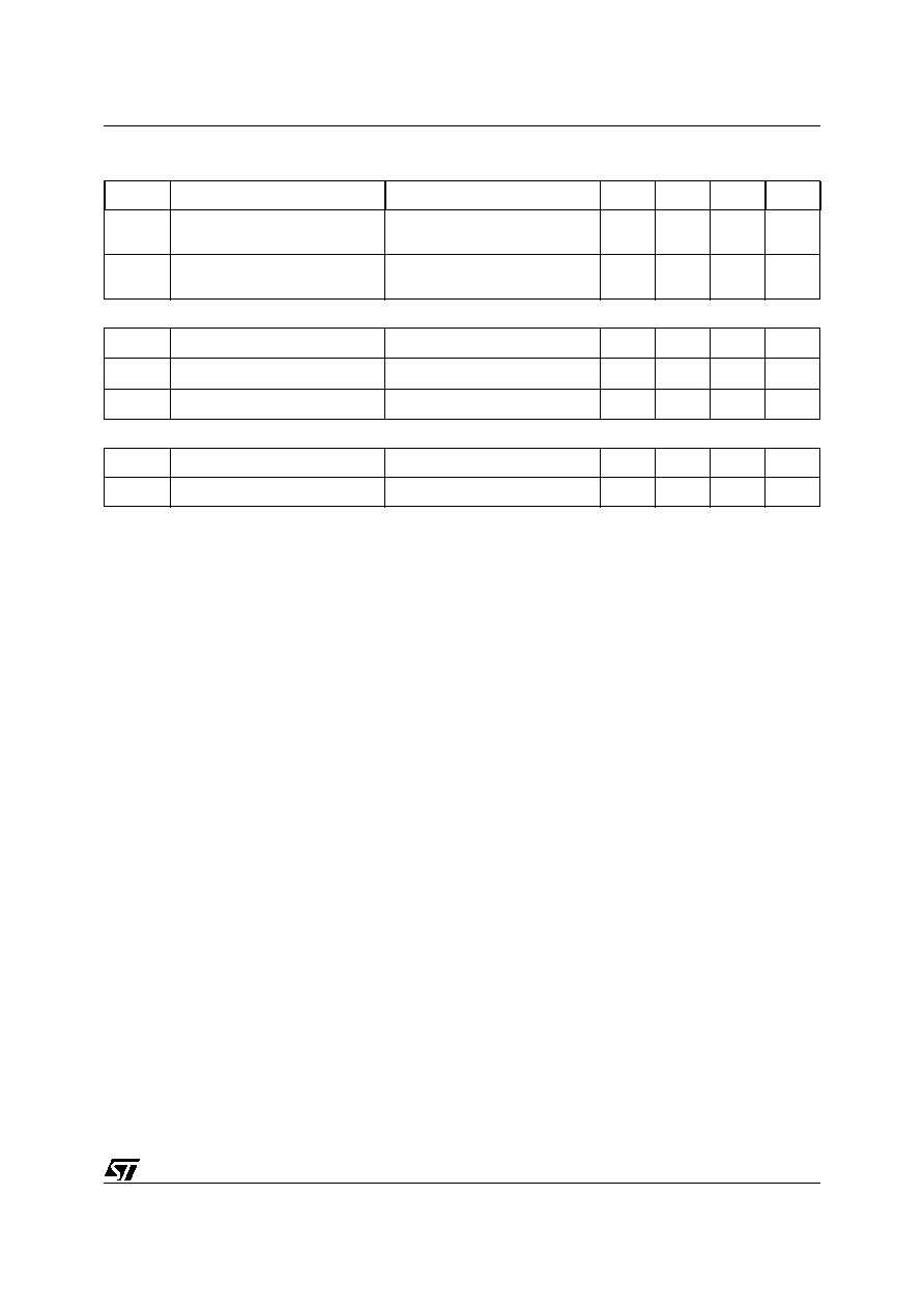
PIN FUNCTIONS
THERMAL DATA
(*) Value depending on PCB copper area and thickness
.
ABSOLUTE MAXIMUM RATINGS
N∞
Pin
Description
1
DRAIN
Drain connection of the internal power MOSFET. The internal high voltage start-up generator
sinks current from this pin.
2
N.C.
Not internally connected. Provision for clearance on the PCB.
3
Vcc
Supply pin of the IC. An electrolytic capacitor is connected between this pin and ground. The
internal start-up generator charges the capacitor until the voltage reaches the start-up threshold.
The PWM is stopped if the voltage at the pin exceeds a certain value.
4
COMP
PWM Control Input. The voltage on this pin (V
COMP
) controls the PWM modulator: the higher
V
COMP
, the higher the duty cycle. The pin will be driven by a current sink (usually the transistor of
an optocoupler) able to modulate V
COMP
by modulating the current.
5
BOK
Brownout Protection. If the voltage applied to this pin is lower than 2.5V the PWM is disabled.
This pin is typically used for sensing the input voltage of the converter through a resistor divider.
If not used, the pin can be either left floating or connected to Vcc through a 15 k
resistor.
6 to 8
GND
Connection of both the source of the internal MOSFET and the return of the bias current of the
IC. Pins connected to the metal frame to facilitate heat dissipation.
Symbol
Parameter
Value
Unit
R
thj-amb
Thermal Resistance Junction-ambient (*)
35 to 60
∞C/W
R
thj-pins
Thermal Resistance Junction-pins
15
∞C/W
Symbol
Parameter
Value
Unit
V
ds
Drain Source Voltage
-0.3 to 700
V
I
d
Drain Current
0.7
A
V
cc
IC Supply Voltage
18
V
I
clamp
V
cc
Zener Current
20
mA
PWM Control Input Sink Current
3
mA
BOK pin Sink Current
1
mA
P
tot
Power Dissipation at T
amb
< 50∞C
3 cm
2
, 2 oz copper dissipating area on PCB
1.5
W
T
j
Operating Junction Temperature
-40 to 150
∞C
T
stg
Storage Temperature
-40 to 150
∞C
L6590A
4/19
ELECTRICAL CHARACTERISTCS (T
j
= -25 to 125∞C, V
cc
= 10V; unless otherwise specified))
Symbol
Parameter
Test Condition
Min.
Typ.
Max.
Unit
POWER SECTION
V
(BR)DSS
Drain Source Voltage
I
d
< 200 µA; T
j
= 25 ∞C
700
V
I
dss
Off state drain current
V
ds
= 560V; T
j
= 125 ∞C
200
µA
R
DS(on)
Drain-to-Source on resistance
R
DS(on)
vs. T
j
: see fig. 17
I
d
= 120mA; T
j
= 25 ∞C
13
16
I
d
= 120mA; T
j
= 125 ∞C
23
28
PWM CONTROL INPUT
V
COMPH
Vout High
I
source
= -0.5mA
3.8
4.5
V
I
COMP
Source Current
1.5V < V
COMP
< 3.5V
-0.5
-1
-2.5
mA
R
COMP
Dynamic Resistance
1.5V < V
COMP
< 3.5V
9
k
OSCILLATOR SECTION
F
osc
Oscillator Frequency
T
j
= 25 ∞C
58
65
72
kHz
52
65
74
D
min
Min. Duty Cycle
V
COMP
= 1V
0
%
D
max
Max. Duty Cycle
V
COMP
= 4V
67
70
73
%
DEVICE OPERATION SECTION
I
op
Operating Supply Current
fsw = Fosc
4.5
7
mA
I
Q
Quiescent Current
MOS disabled
3.5
6
mA
I
charge
V
CC
charge Current
V
cc
= 0V to V
ccon
- 0.5V;
V
ds
= 100 to 400V; T
j
= 25∞C
-3
-4.5
-7
mA
V
cc
= 0V to V
ccon
- 0.5V;
V
ds
= 100 to 400V
-2.5
-4.5
-7.5
mA
V
CCclamp
V
CC
Clamp Voltage
I
clamp
= 10mA (*)
15.5
16.5
17.5
V
V
ccon
Start Threshold
voltage
(*)
13.5
14.5
15.5
V
V
ccoff
Min operating voltage after Turn
on
(*)
6
6.6
7.2
V
V
dsmin
Drain start voltage
40
V
CIRCUIT PROTECTIONS
I
pklim
Pulse-by-pulse Current Limit
di/dt = 120 mA/ µs
550
625
700
mA
V
ccOVP
Overvoltage Protection
I
cc
= 10 mA (*)
15
16
17
V
LEB
Masking Time
After MOSFET turn-on (**)
120
ns
STANDBY SECTION
F
SB
Oscillator Frequency
19
22
25
kHz
5/19
L6590A
(*) Parameters tracking one the other
(**) Parameter guaranteed by design, not tested in production
(***) Parameters guaranteed by design, functionality tested in production
I
pksb
Peak switch current for Standby
Operation
Transition from F
osc
to F
SB
80
mA
I
pkno
Peak switch current for Normal
Operation
Transition from F
SB
to F
osc
190
mA
BROWNOUT PROTECTION
V
th
Threshold Voltage
Voltage either rising or falling
2.325
2.5
2.675
V
I
Hys
Current Hysteresis
V
pin
= 3V
-30
-50
-70
µA
V
CL
Clamp Voltage
I
pin
= 0.5 mA
5.6
6.4
7.2
V
THERMAL SHUTDOWN (***)
Threshold
150
165
∞C
Hysteresis
40
∞C
Symbol
Parameter
Test Condition
Min.
Typ.
Max.
Unit
ELECTRICAL CHARACTERISTICS (continued)